EP0633512A2 - Dispositif de chargement d'un appareil pour former une image - Google Patents
Dispositif de chargement d'un appareil pour former une image Download PDFInfo
- Publication number
- EP0633512A2 EP0633512A2 EP94304985A EP94304985A EP0633512A2 EP 0633512 A2 EP0633512 A2 EP 0633512A2 EP 94304985 A EP94304985 A EP 94304985A EP 94304985 A EP94304985 A EP 94304985A EP 0633512 A2 EP0633512 A2 EP 0633512A2
- Authority
- EP
- European Patent Office
- Prior art keywords
- charging device
- image carrier
- charging
- fibrous member
- conductive
- Prior art date
- Legal status (The legal status is an assumption and is not a legal conclusion. Google has not performed a legal analysis and makes no representation as to the accuracy of the status listed.)
- Granted
Links
- 239000004745 nonwoven fabric Substances 0.000 claims abstract description 10
- 239000002759 woven fabric Substances 0.000 claims 1
- 238000000034 method Methods 0.000 description 17
- CBENFWSGALASAD-UHFFFAOYSA-N Ozone Chemical compound [O-][O+]=O CBENFWSGALASAD-UHFFFAOYSA-N 0.000 description 8
- 239000000853 adhesive Substances 0.000 description 8
- 230000001070 adhesive effect Effects 0.000 description 8
- 229910052751 metal Inorganic materials 0.000 description 7
- 239000002184 metal Substances 0.000 description 7
- 239000000835 fiber Substances 0.000 description 6
- 229920001940 conductive polymer Polymers 0.000 description 3
- 238000007599 discharging Methods 0.000 description 3
- 239000000945 filler Substances 0.000 description 3
- 239000000463 material Substances 0.000 description 3
- 238000009987 spinning Methods 0.000 description 3
- OKTJSMMVPCPJKN-UHFFFAOYSA-N Carbon Chemical compound [C] OKTJSMMVPCPJKN-UHFFFAOYSA-N 0.000 description 2
- XEEYBQQBJWHFJM-UHFFFAOYSA-N Iron Chemical compound [Fe] XEEYBQQBJWHFJM-UHFFFAOYSA-N 0.000 description 2
- -1 acryl Chemical group 0.000 description 2
- 229910052782 aluminium Inorganic materials 0.000 description 2
- XAGFODPZIPBFFR-UHFFFAOYSA-N aluminium Chemical compound [Al] XAGFODPZIPBFFR-UHFFFAOYSA-N 0.000 description 2
- 229910052799 carbon Inorganic materials 0.000 description 2
- 238000001035 drying Methods 0.000 description 2
- 230000000694 effects Effects 0.000 description 2
- 230000001788 irregular Effects 0.000 description 2
- 238000004519 manufacturing process Methods 0.000 description 2
- 230000003287 optical effect Effects 0.000 description 2
- 230000002093 peripheral effect Effects 0.000 description 2
- 239000005020 polyethylene terephthalate Substances 0.000 description 2
- 229920002717 polyvinylpyridine Polymers 0.000 description 2
- 239000004065 semiconductor Substances 0.000 description 2
- 229910001220 stainless steel Inorganic materials 0.000 description 2
- 239000010935 stainless steel Substances 0.000 description 2
- 239000000126 substance Substances 0.000 description 2
- WFKWXMTUELFFGS-UHFFFAOYSA-N tungsten Chemical compound [W] WFKWXMTUELFFGS-UHFFFAOYSA-N 0.000 description 2
- 229910052721 tungsten Inorganic materials 0.000 description 2
- 239000010937 tungsten Substances 0.000 description 2
- 239000004593 Epoxy Substances 0.000 description 1
- 239000004677 Nylon Substances 0.000 description 1
- 229920000297 Rayon Polymers 0.000 description 1
- BUGBHKTXTAQXES-UHFFFAOYSA-N Selenium Chemical compound [Se] BUGBHKTXTAQXES-UHFFFAOYSA-N 0.000 description 1
- BQCADISMDOOEFD-UHFFFAOYSA-N Silver Chemical compound [Ag] BQCADISMDOOEFD-UHFFFAOYSA-N 0.000 description 1
- 230000015572 biosynthetic process Effects 0.000 description 1
- 238000004140 cleaning Methods 0.000 description 1
- 238000010276 construction Methods 0.000 description 1
- 229910052802 copper Inorganic materials 0.000 description 1
- 230000007547 defect Effects 0.000 description 1
- 230000002950 deficient Effects 0.000 description 1
- 239000000428 dust Substances 0.000 description 1
- 230000002708 enhancing effect Effects 0.000 description 1
- 238000002474 experimental method Methods 0.000 description 1
- 239000004744 fabric Substances 0.000 description 1
- 239000002657 fibrous material Substances 0.000 description 1
- 229910052742 iron Inorganic materials 0.000 description 1
- 238000002844 melting Methods 0.000 description 1
- 230000008018 melting Effects 0.000 description 1
- 238000012986 modification Methods 0.000 description 1
- 230000004048 modification Effects 0.000 description 1
- 229910052759 nickel Inorganic materials 0.000 description 1
- 229920001778 nylon Polymers 0.000 description 1
- 239000011148 porous material Substances 0.000 description 1
- 238000003825 pressing Methods 0.000 description 1
- 239000002994 raw material Substances 0.000 description 1
- 239000002964 rayon Substances 0.000 description 1
- 239000011347 resin Substances 0.000 description 1
- 229920005989 resin Polymers 0.000 description 1
- 229910052711 selenium Inorganic materials 0.000 description 1
- 239000011669 selenium Substances 0.000 description 1
- 229910052709 silver Inorganic materials 0.000 description 1
- 239000004332 silver Substances 0.000 description 1
- XLYOFNOQVPJJNP-UHFFFAOYSA-N water Substances O XLYOFNOQVPJJNP-UHFFFAOYSA-N 0.000 description 1
Images


Classifications
-
- G—PHYSICS
- G03—PHOTOGRAPHY; CINEMATOGRAPHY; ANALOGOUS TECHNIQUES USING WAVES OTHER THAN OPTICAL WAVES; ELECTROGRAPHY; HOLOGRAPHY
- G03G—ELECTROGRAPHY; ELECTROPHOTOGRAPHY; MAGNETOGRAPHY
- G03G15/00—Apparatus for electrographic processes using a charge pattern
- G03G15/02—Apparatus for electrographic processes using a charge pattern for laying down a uniform charge, e.g. for sensitising; Corona discharge devices
- G03G15/0208—Apparatus for electrographic processes using a charge pattern for laying down a uniform charge, e.g. for sensitising; Corona discharge devices by contact, friction or induction, e.g. liquid charging apparatus
-
- G—PHYSICS
- G03—PHOTOGRAPHY; CINEMATOGRAPHY; ANALOGOUS TECHNIQUES USING WAVES OTHER THAN OPTICAL WAVES; ELECTROGRAPHY; HOLOGRAPHY
- G03G—ELECTROGRAPHY; ELECTROPHOTOGRAPHY; MAGNETOGRAPHY
- G03G15/00—Apparatus for electrographic processes using a charge pattern
- G03G15/02—Apparatus for electrographic processes using a charge pattern for laying down a uniform charge, e.g. for sensitising; Corona discharge devices
- G03G15/0291—Apparatus for electrographic processes using a charge pattern for laying down a uniform charge, e.g. for sensitising; Corona discharge devices corona discharge devices, e.g. wires, pointed electrodes, means for cleaning the corona discharge device
Definitions
- the present invention relates to an electrophotographic image forming apparatus having an image carrier for forming an electrostatic latent image thereon and, more particularly, to a charging device for charging the image carrier.
- Electrophotographic copiers, laser printers and facsimile machines belong to a family of electrophotographic image forming apparatuses having an image carrier in the form of a photoconductive drum or a photoconductive belt.
- Electrophotographic methods for this type of image forming apparatus include an indirect electrophotographic method which charges the surface of the image carrier uniformly, exposes the charged surface to image data, e.g., a reflection from an original document to form an electrostatic latent image thereon, develops the latent image by a toner or similar developer, transfers the resulting toner image to a plain paper or similar recording medium, and then fixes the toner image on the medium by heat and pressure.
- a direct electrophotographic method is another conventional electrophotographic method and uses a recording medium itself as an image carrier. This kind of method charges the surface of the medium uniformly and then sequentially executes the exposing, developing and fixing steps with the medium. In any case, the electrophotographic method charges the surface of the image carrier uniformly at the beginning of image formation.
- a corona discharge type charging device deposits a charge on the surface of the image carrier with one or more wires for corona discharge.
- this type of device has a shield having an opening facing the image carrier, and one or more tungsten wires or gold-plated tungsten wires disposed in the shield.
- a high voltage of 4 kV to 7 kV in absolute value is applied to the wires to effect corona discharge.
- a scorotron charger is provided with a grid electrode between the wires and the image carrier in order to promote uniform and stable charging.
- a brush type charging device has a conductive brush connected to a power source and made of metal or conductive resin. The brush is held in contact with the image carrier for charging the surface of the image carrier.
- This type of device differs from the corona discharge type device in that it is operable with a relatively low voltage which is substantially the same in potential as a target charge level.
- a roller type charging device uses a roller consisting of a metallic shaft and one or more layers of conductive rubber covering the shaft. This type of device applies a voltage to the roller while pressing it against the image carrier.
- Such a charging device like the brush type charging device, can operate with a relatively low voltage and, in addition, produces only a small amount of ozone.
- the corona discharge type device needs a voltage as high as 4 kV to 7 kV in absolute value.
- the wiring for the device has to be connected and distinguished from the other wirings with greatest care.
- corona discharge produces ozone.
- negative corona discharge produces more than ten times of ozone than positive corona discharge.
- Such an amount of ozone limits materials available for the parts built in the image forming apparatus as well as reliability of operation.
- an ozone filter is needed and has to be replaced often, increasing the running cost of the apparatus.
- products deposited on the wire surfaces due to corona discharge degrade the discharging ability and, therefore, reliability of the discharging device itself.
- the brush type and the roller type discharging devices produce a minimum of ozone, they are apt to scratch the surface of the image carrier since the former contacts the latter. Further, the conductive brush, for example, is smeared due to the defective cleaning of the image carrier and the entry of developer and paper dust in the charging device, resulting in the fall of charge potential. Irregular charging is also brought about by irregularities particular to production and assembly lines. Particularly, the brush type charging device has various problems relating to the density of the brush, the fall-out of bristles, and the conditions for the contact of the brush with the image carrier. Although a charging device using a multi-stage brush scheme has been proposed, it is also problematic in respect of cost and space.
- the roller type charging device can obviate many of the problems of the brush type charging device. This, coupled with the fact that rollers of uniform configuration can be produced relatively easily and can be uniformly pressed against the image carrier, has put the roller type device to practical use. However, once the surface of the roller is scratched or otherwise disfigured, image quality is lowered since the disfigured portion differs in charging ability from the other portion. Also, this type of charging device is questionable as to whether or not it can implement further uniform charging matching the increasing image density. In addition, such a device is not applicable to a multicolor developing process which forms color images one above the other on the image carrier.
- the charging member includes a conductive support and a conductive fibrous member affixed to the surface of the conductive support which faces the image carrier.
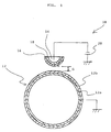
- a charging device embodying the present invention is shown and generally designated by the reference numeral 10.
- the charging device 10 has a semicylindrical metallic support 14 having a semicircular cross-section.
- the metallic support 14 faces and extends parallel to a photoconductive drum, or image carrier, 12.
- a conductive fibrous member 16 is affixed to the surface of the support 14 which faces the drum 12 by a conductive adhesive 18.
- a power source 20 is connected to the support 14.
- a gap G is defined between the fibrous member 16 and the drum 12.
- the conductive fibrous member 16 may be implemented by any suitable conductive fibrous material.
- any suitable conductive fibrous material For example, use may advantageously be made of an nonwoven fabric, a regularly woven webbing, or electrically implanted bristles treated for electric conduction.
- the nonwoven fabric or the regularly woven webbing may be comprised of a webbing plated or coated with metal or conductive polymer for electric conduction.
- the electrically implanted bristles bristles may be provided on a support and then treated for conduction.
- the nonwoven fabric may be implemented by fibers having a diameter of less than several microns and including of one or more of poly-ethylene-terephthalate (PET), polyvinylpyridine (PP), rayon, nylon, acryl or similar substance as a base material.
- PET poly-ethylene-terephthalate
- PP polyvinylpyridine
- rayon rayon
- nylon acryl or similar substance
- the fabric is coated with Ni, Cu or similar metal or with a conductive polymer containing a metal filler and carbon.
- a wet process method disperses short fibers in water by a spinning system and dehydrates and dries them.
- the dry process method forms a webbing by ordinary spinning or special spinning, e.g., a parallel method of a raw material and then bonds it by melting, chemical and mechanical adhesion and confounding.
- a regularly woven webbing may also be implemented by the above-mentioned fibers and provided with conductivity by the above-mentioned procedure.
- electrically implanted bristles they may be provided on a support made of stainless steel or similar material and then coated with metal or conductive polymer.
- the conductive fibrous member 16 usually has, when affixed to the support 14, a thickness of 40 ⁇ m to 3000 ⁇ m, preferably 500 ⁇ m to 1000 ⁇ m, and a weight of 20 g/m2 to 2000 g/m2, preferably 90 g/m2 to 200 g/m2.
- the fibers constituting the fibrous member 16 usually have a diameter ranging from 0.02 ⁇ m to 50 ⁇ m, preferably from 0.1 ⁇ m to 10 ⁇ m. Diameters smaller than 0.02 ⁇ m would only make it difficult to form a needle electrode structure. Diameters greater than 50 ⁇ m would make the resulting webbing difficult to handle and prevent it from being uniformly attached to the support 14.
- the electric resistance of the fibrous member 16 should preferably be 101 ⁇ cm to 1010 ⁇ cm in terms of volume resistivity.
- FIG. 2 shows the results of experiments conducted with the charging device 10.
- the charge potential deposited on the drum 12 changes with changes in resistance and voltage applied.
- a charge potential of -600 V. for example is achievable with a voltage of about -1200 V to -2000 V.
- electric resistance lower than 101 ⁇ c m cannot deposit the required potential while electric resistance higher than 1010 ⁇ cm cannot provide the charge potential of -600 V without resorting to a high voltage.
- the metallic support 14 is comprised of, but not limited to, iron, aluminum, stainless steel or similar metal.
- the conductive adhesive 18 use may be made of, for example, an epoxy-based adhesive containing a silver filler or an acryl-based adhesive containing a carbon filler.
- the fibrous member 16 is uniformly affixed to the surface of the support 14 which faces the drum 12 by the adhesive 18, as stated earlier.
- a nonwoven fabric itself is conductive and has numerous pores due to the structure particular thereto. In light of this, a nonwoven fabric may be impregnated with the previously mentioned ordinary insulative adhesive; the conductive fibers will contact the object in the event of adhesion.
- the gap G between the fibrous member 16 and the drum 12 ranges from 0.15 mm to 3.5 mm, preferably 0.2 mm to 2.5 mm.
- FIG. 3 shows a relation between the charge potential and the voltage applied. As shown, the smaller the gap G and the higher the voltage, the higher the charge potential in absolute value. Gaps G smaller than 0.15 mm would be apt to cause the fibers of the fibrous member 16 to contact the drum 12, while gaps G greater than 3.5 mm would obstruct sufficient charging.
- FIGS. 2 and 3 teach that when the electric resistance is 101 ⁇ cm and the gap G is 0.5 mm, a voltage of -1250 V suffices.
- the power source 20 is connected to the metallic support 14 and applies the voltage to the fibrous member 16 via the support 14.
- the drum 12 may be replaced with any other suitable form of latent image carrier customary with an electrophotographic method, e.g., a photoconductive belt.
- the drum 12 usually has a base 12a made of aluminum or similar metal and a photoconductive layer 12b provided on the base 12a.
- the metallic base 12a is connected to ground.
- the photoconductive layer 12b is implemented as one or more layers of, for example, selenium-based metallic optical semiconductor or organic optical semiconductor.
- the drum 12 has the surface thereof discharged.
- the conductive fibrous member 16 connected to the power source 20, effects a fine discharge toward the drum 12 via the gap G. This is because the surface of the fibrous member 16 plays the role of needle electrodes. As a result, the surface of the drum 12 is uniformly charged.
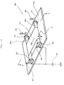
- the charging device generally 30, has a metallic support in the form of a thin flexible seamless belt 32, and a tape-like conductive fibrous member 34 spirally wrapped around the belt 32 with the intermediary of a conductive adhesive 36.
- the support 32 is passed over two metallic shafts 38a and 38b and held under suitable tension.
- the fibrous member 34 is located to face a latent image carrier 40.
- Rollers 42 are respectively affixed to the opposite ends of the two shafts 38a and 38b so as to maintain a gap G between the surface of the latent image carrier 40 and that of the fibrous member 34.
- the rollers 42 and shafts 38a and 38b are rotatable integrally with each other when the latent image carrier 40 is moved.
- Springs 44 are respectively anchored to the opposite ends of the shafts 38a and 38b, so that the rollers 42 are constantly urged against the latent image carrier 40.
- a power source 46 is connected to the shafts 38a and 38b.
- the fibrous member 34 is affixed to the outer periphery of the support 32 by the adhesive 36, as in the previous embodiment.
- the charging device 30 charges the latent image carrier 40 in the same manner as in the previous embodiment.
- the gap G i.e., gaps a and b formed in the direction in which the latent image carrier 40 and fibrous member 34 move relative to each other remain constant.
- the rollers 42 and shafts 38a and 38b are rotated.
- the fibrous member 34 moves downstream in the surface area of the latent image carrier 4 0 while, at the same time, the surface of the image carrier 40 facing the fibrous member 34 changes.
- this embodiment is capable of charging the image carrier 40 over a broad area.
- the surface of the fibrous member 34 sequentially changes, uniform and stable charging is insured despite smears and defects which may exist on the fibrous member 34.
- the peripheral speed of the fibrous member, or thin flexible seamless belt, 34 is open to choice, it should preferably be higher than the peripheral speed of the image carrier 40 in order to promote uniform charging.
- the fibrous member 34 is implemented by a nonwoven fabric treated for conduction, a regularly woven webbing, or electrically implanted bristles, as in the previous embodiment.
- the power sources 20 and 46 are each assumed to be a DC power source.
- an AC voltage having a peak-to-peak voltage twice as high as the DC voltage to be initially applied and having a frequency of 20 Hz to 1000 Hz, preferably, 100 Hz to 500 Hz may be superposed on the DC voltage.
- Such an AC-biased DC voltage will cause charging and reverse charging to occur alternately, thereby reducing local irregular charging.
- the present system provides a charging device which can charge an image carrier without contacting it and is, therefore, advantageous over a conventional contact type charging device in respect of resistivity to smears, reliability and uniform charging.
- the charging device is operable with a voltage lower than the voltage conventionally applied to a corona charger, it causes less ozone to be produced while enhancing safety operation.
- the charging device is reliable and charges the image carrier in a stable manner at all times, thereby providing high quality images. Nevertheless it is relatively simple in construction and is inexpensive.
Landscapes
- Physics & Mathematics (AREA)
- Engineering & Computer Science (AREA)
- Plasma & Fusion (AREA)
- General Physics & Mathematics (AREA)
- Electrostatic Charge, Transfer And Separation In Electrography (AREA)
Applications Claiming Priority (2)
| Application Number | Priority Date | Filing Date | Title |
|---|---|---|---|
| JP166733/93 | 1993-07-06 | ||
| JP5166733A JPH0720681A (ja) | 1993-07-06 | 1993-07-06 | 帯電装置 |
Publications (3)
| Publication Number | Publication Date |
|---|---|
| EP0633512A2 true EP0633512A2 (fr) | 1995-01-11 |
| EP0633512A3 EP0633512A3 (fr) | 1995-02-22 |
| EP0633512B1 EP0633512B1 (fr) | 1998-10-28 |
Family
ID=15836746
Family Applications (1)
| Application Number | Title | Priority Date | Filing Date |
|---|---|---|---|
| EP94304985A Expired - Lifetime EP0633512B1 (fr) | 1993-07-06 | 1994-07-06 | Dispositif de chargement d'un appareil pour former une image |
Country Status (4)
| Country | Link |
|---|---|
| US (1) | US5483324A (fr) |
| EP (1) | EP0633512B1 (fr) |
| JP (1) | JPH0720681A (fr) |
| DE (1) | DE69414191T2 (fr) |
Families Citing this family (5)
| Publication number | Priority date | Publication date | Assignee | Title |
|---|---|---|---|---|
| JP3507222B2 (ja) * | 1995-10-26 | 2004-03-15 | キヤノン株式会社 | トナー補給容器 |
| JP3471992B2 (ja) * | 1995-10-26 | 2003-12-02 | キヤノン株式会社 | トナー補給容器及び画像形成装置 |
| JP2002055512A (ja) * | 2000-05-30 | 2002-02-20 | Ricoh Co Ltd | 帯電装置および該帯電装置を有する画像形成装置 |
| US6907208B2 (en) | 2002-10-25 | 2005-06-14 | Michael E. Bausch | Developer cartridge including sealing gasket |
| US7964012B2 (en) | 2005-08-03 | 2011-06-21 | Hollingsworth & Vose Company | Filter media with improved conductivity |
Family Cites Families (12)
| Publication number | Priority date | Publication date | Assignee | Title |
|---|---|---|---|---|
| US2934649A (en) * | 1957-01-09 | 1960-04-26 | Haloid Xerox Inc | Induction charging |
| DE1128293B (de) * | 1959-11-18 | 1962-04-19 | Bayer Ag | Vorrichtung zur elektrophotographischen Herstellung von Bildern |
| DE3164262D1 (en) * | 1980-03-10 | 1984-07-26 | Tokyo Shibaura Electric Co | Charging device |
| US4555171A (en) * | 1982-03-15 | 1985-11-26 | Schlegel Corporation | Conductive charge/discharge device |
| SU1068883A1 (ru) * | 1982-09-17 | 1984-01-23 | Специализированное конструкторско-технологическое бюро "Оптоэлектроника" при Кишиневском государственном университете им.В.И.Ленина | Устройство коронной зар дки электрофотографических носителей записи |
| JPS6343749A (ja) * | 1986-08-12 | 1988-02-24 | Nippon Kokan Kk <Nkk> | 移動鋳型式連続鋳造用溶融金属注入ノズル |
| JPS6394257A (ja) * | 1986-10-08 | 1988-04-25 | Nec Corp | 電子写真式記録方式 |
| JPS62168171A (ja) * | 1986-12-26 | 1987-07-24 | Toshiba Corp | 帯電装置 |
| JP2557487B2 (ja) * | 1988-08-20 | 1996-11-27 | 富士通株式会社 | 個人照合装置 |
| JPH04240670A (ja) * | 1991-01-24 | 1992-08-27 | Canon Inc | 帯電装置及びこれを備えた画像形成装置 |
| JP2619154B2 (ja) * | 1991-06-28 | 1997-06-11 | 株式会社東芝 | 画像形成装置 |
| JPH0627781A (ja) * | 1992-07-09 | 1994-02-04 | Brother Ind Ltd | 帯電装置 |
-
1993
- 1993-07-06 JP JP5166733A patent/JPH0720681A/ja active Pending
-
1994
- 1994-07-06 EP EP94304985A patent/EP0633512B1/fr not_active Expired - Lifetime
- 1994-07-06 US US08/267,206 patent/US5483324A/en not_active Expired - Lifetime
- 1994-07-06 DE DE69414191T patent/DE69414191T2/de not_active Expired - Lifetime
Also Published As
| Publication number | Publication date |
|---|---|
| EP0633512A3 (fr) | 1995-02-22 |
| DE69414191D1 (de) | 1998-12-03 |
| US5483324A (en) | 1996-01-09 |
| DE69414191T2 (de) | 1999-06-24 |
| JPH0720681A (ja) | 1995-01-24 |
| EP0633512B1 (fr) | 1998-10-28 |
Similar Documents
| Publication | Publication Date | Title |
|---|---|---|
| US5091751A (en) | Image forming apparatus utilizing intermediate transfer member | |
| US5249022A (en) | Image forming device having an electrically dielectric regulating member conductive transfer member and a disposed at a transfer station thereof | |
| US5221946A (en) | Image forming apparatus | |
| KR920003245B1 (ko) | 현상장치 | |
| EP0458273A2 (fr) | Dispositif de chargement, appareil de formation d'images avec un tel dispositif et unité de traitement montée de manière amovible dans l'appareil de formation d'images | |
| US5678136A (en) | Image forming apparatus with charging member supplied with first and second DC voltages of opposite polarities | |
| US7113726B2 (en) | Charging device, image forming process cartridge, and image forming apparatus including the charging device | |
| EP0431559B1 (fr) | Appareil de formation d'images comprenant des moyens de chargement | |
| EP0633512B1 (fr) | Dispositif de chargement d'un appareil pour former une image | |
| JPH1073983A (ja) | 画像形成装置 | |
| EP0590912A2 (fr) | Méthode de chargement par contact de la surface d'un matériau photosensible | |
| US5473414A (en) | Cleaning commutator brushes for an electroded donor roll | |
| JPH07155222A (ja) | クリーニングブラシ | |
| US5410390A (en) | Image forming apparatus having transfer material carrying member with specific resistance ratio | |
| US6128460A (en) | Image forming system for conveying recording material | |
| JP3491458B2 (ja) | 画像形成装置 | |
| JPH0822232A (ja) | 画像形成装置 | |
| EP0496399A2 (fr) | Dispositif de chargement disposé près de l'élément à charger et appareil de formation d'images utilisant un tel dispositif | |
| JPH04345186A (ja) | 画像形成装置 | |
| JPS63210864A (ja) | 画像形成装置 | |
| JP3449167B2 (ja) | 帯電装置 | |
| JPH0627782A (ja) | 帯電装置 | |
| JPH04186387A (ja) | 画像形成装置 | |
| JPH06295117A (ja) | 画像形成装置 | |
| JPH02282279A (ja) | 接触帯電装置 |
Legal Events
| Date | Code | Title | Description |
|---|---|---|---|
| PUAI | Public reference made under article 153(3) epc to a published international application that has entered the european phase |
Free format text: ORIGINAL CODE: 0009012 |
|
| PUAL | Search report despatched |
Free format text: ORIGINAL CODE: 0009013 |
|
| AK | Designated contracting states |
Kind code of ref document: A2 Designated state(s): DE GB IT |
|
| AK | Designated contracting states |
Kind code of ref document: A3 Designated state(s): DE GB IT |
|
| 17P | Request for examination filed |
Effective date: 19950117 |
|
| 17Q | First examination report despatched |
Effective date: 19960820 |
|
| GRAG | Despatch of communication of intention to grant |
Free format text: ORIGINAL CODE: EPIDOS AGRA |
|
| GRAG | Despatch of communication of intention to grant |
Free format text: ORIGINAL CODE: EPIDOS AGRA |
|
| GRAH | Despatch of communication of intention to grant a patent |
Free format text: ORIGINAL CODE: EPIDOS IGRA |
|
| GRAH | Despatch of communication of intention to grant a patent |
Free format text: ORIGINAL CODE: EPIDOS IGRA |
|
| GRAA | (expected) grant |
Free format text: ORIGINAL CODE: 0009210 |
|
| AK | Designated contracting states |
Kind code of ref document: B1 Designated state(s): DE GB IT |
|
| REF | Corresponds to: |
Ref document number: 69414191 Country of ref document: DE Date of ref document: 19981203 |
|
| ITF | It: translation for a ep patent filed | ||
| PLBE | No opposition filed within time limit |
Free format text: ORIGINAL CODE: 0009261 |
|
| STAA | Information on the status of an ep patent application or granted ep patent |
Free format text: STATUS: NO OPPOSITION FILED WITHIN TIME LIMIT |
|
| 26N | No opposition filed | ||
| REG | Reference to a national code |
Ref country code: GB Ref legal event code: 732E |
|
| REG | Reference to a national code |
Ref country code: GB Ref legal event code: IF02 |
|
| PGFP | Annual fee paid to national office [announced via postgrant information from national office to epo] |
Ref country code: DE Payment date: 20130703 Year of fee payment: 20 |
|
| PGFP | Annual fee paid to national office [announced via postgrant information from national office to epo] |
Ref country code: GB Payment date: 20130703 Year of fee payment: 20 |
|
| PGFP | Annual fee paid to national office [announced via postgrant information from national office to epo] |
Ref country code: IT Payment date: 20130711 Year of fee payment: 20 |
|
| REG | Reference to a national code |
Ref country code: DE Ref legal event code: R071 Ref document number: 69414191 Country of ref document: DE |
|
| REG | Reference to a national code |
Ref country code: GB Ref legal event code: PE20 Expiry date: 20140705 |
|
| PG25 | Lapsed in a contracting state [announced via postgrant information from national office to epo] |
Ref country code: DE Free format text: LAPSE BECAUSE OF EXPIRATION OF PROTECTION Effective date: 20140708 |
|
| PG25 | Lapsed in a contracting state [announced via postgrant information from national office to epo] |
Ref country code: GB Free format text: LAPSE BECAUSE OF EXPIRATION OF PROTECTION Effective date: 20140705 |