EP0633656A2 - MOS differential voltage-to-current converter circuit - Google Patents
MOS differential voltage-to-current converter circuit Download PDFInfo
- Publication number
- EP0633656A2 EP0633656A2 EP94110371A EP94110371A EP0633656A2 EP 0633656 A2 EP0633656 A2 EP 0633656A2 EP 94110371 A EP94110371 A EP 94110371A EP 94110371 A EP94110371 A EP 94110371A EP 0633656 A2 EP0633656 A2 EP 0633656A2
- Authority
- EP
- European Patent Office
- Prior art keywords
- mos
- current
- mos transistors
- differential
- converter circuit
- Prior art date
- Legal status (The legal status is an assumption and is not a legal conclusion. Google has not performed a legal analysis and makes no representation as to the accuracy of the status listed.)
- Granted
Links
- 230000008054 signal transmission Effects 0.000 claims abstract description 34
- 238000006243 chemical reaction Methods 0.000 abstract 1
- 238000010276 construction Methods 0.000 description 55
- 230000000694 effects Effects 0.000 description 5
- 230000005669 field effect Effects 0.000 description 4
- 238000004519 manufacturing process Methods 0.000 description 4
- 230000003321 amplification Effects 0.000 description 3
- 238000010586 diagram Methods 0.000 description 3
- 238000000034 method Methods 0.000 description 3
- 238000003199 nucleic acid amplification method Methods 0.000 description 3
- 229920006395 saturated elastomer Polymers 0.000 description 3
- 230000003247 decreasing effect Effects 0.000 description 2
- 238000009738 saturating Methods 0.000 description 2
- 239000004065 semiconductor Substances 0.000 description 2
- 239000008186 active pharmaceutical agent Substances 0.000 description 1
- 238000007792 addition Methods 0.000 description 1
- 230000015556 catabolic process Effects 0.000 description 1
- 238000006731 degradation reaction Methods 0.000 description 1
- 230000000630 rising effect Effects 0.000 description 1
Images









Classifications
-
- H—ELECTRICITY
- H02—GENERATION; CONVERSION OR DISTRIBUTION OF ELECTRIC POWER
- H02M—APPARATUS FOR CONVERSION BETWEEN AC AND AC, BETWEEN AC AND DC, OR BETWEEN DC AND DC, AND FOR USE WITH MAINS OR SIMILAR POWER SUPPLY SYSTEMS; CONVERSION OF DC OR AC INPUT POWER INTO SURGE OUTPUT POWER; CONTROL OR REGULATION THEREOF
- H02M11/00—Power conversion systems not covered by the preceding groups
-
- H—ELECTRICITY
- H03—ELECTRONIC CIRCUITRY
- H03F—AMPLIFIERS
- H03F3/00—Amplifiers with only discharge tubes or only semiconductor devices as amplifying elements
- H03F3/45—Differential amplifiers
- H03F3/45071—Differential amplifiers with semiconductor devices only
- H03F3/45076—Differential amplifiers with semiconductor devices only characterised by the way of implementation of the active amplifying circuit in the differential amplifier
- H03F3/45179—Differential amplifiers with semiconductor devices only characterised by the way of implementation of the active amplifying circuit in the differential amplifier using MOSFET transistors as the active amplifying circuit
- H03F3/45197—Pl types
-
- H—ELECTRICITY
- H03—ELECTRONIC CIRCUITRY
- H03F—AMPLIFIERS
- H03F1/00—Details of amplifiers with only discharge tubes, only semiconductor devices or only unspecified devices as amplifying elements
- H03F1/32—Modifications of amplifiers to reduce non-linear distortion
- H03F1/3211—Modifications of amplifiers to reduce non-linear distortion in differential amplifiers
Definitions
- the present invention relates to a MOS voltage-to-current converter circuit employing a field-effect MOS transistor formed on a semiconductor integrated circuit chip. More specifically, the invention relates to a MOS differential voltage-to-current converter circuit which suppresses fluctuation of a mutual conductance.
- MOSFET field-effect MOS transistor
- NMOSFET N-channel field - effect MOS transistor
- PMOSFET P-channel field-effect MOS transistor
- I, I*, I**, ⁇ I represent current
- V, V*, V**, ⁇ V represent voltage
- R, R*, R** represent resistance
- ⁇ , ⁇ * represent gain coefficient of MOSFET
- gm, gm* represent mutual conductance of the differential voltage-to-current converter circuit.
- *,** represent numerals.
- N1 and N2 represent first and second NMOSFET
- 2R0 represents one source resistance (resistance value 2R0) mutually connecting the source terminals of N1 and N2.
- V1 and V2 represent first and second input voltages of the differential voltage-to-current converter circuit
- V B1 and V B2 represent backgate voltages
- I01 and I02 represent first and second constant current sources, respectively.
- I1 and I2 represent first and second output currents of the differential voltage-current converter circuit, respectively.
- the differential input voltage ⁇ V can be expressed by the following equation (6) with taking the current flowing through a resistor 2R0 between the sources being I R0 . It should be appreciated that, the gain coefficients ⁇ of N1 and N2 forming a differential pair in the equation (6) are mutually equal.
- a reciprocal of the mutual conductance g m of the differential voltage-to-current converter circuit can be obtained by differentiating ⁇ V with the differential output current ⁇ I , and expressed by the following equation (9) .
- the mutual conductance g m becomes the maximum value g mmax when the differential input voltage ⁇ V is 0.
- ⁇ I becomes 0, the reciprocal of the maximum value g mmax is expressed by the following equation (10).
- a coefficient E expressing non-linearity of the input/output characteristics of the differential voltage-to-current converter circuit is defined by the equation (12-a). Namely, the non-linearity E can be obtained by obtaining a difference between the input/output characteristics curve a and the tangent b with respect to ⁇ V and by dividing the difference by the value (g mmax x ⁇ V) of the tangent b.
- the non-linearity E can be expressed with the coefficient ⁇ and I00 in the following equation (12-b).
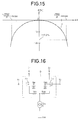
- a curve in Fig. 15 is a plot of the non-linearity with respect to the differential input voltage ⁇ V (horizontal axis).
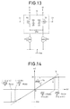
- Figs. 16 shows another example of a circuit construction of the conventional the differential voltage-to-current converter circuit in which first and second resistors R01 and R02 are connected in common (hereinafter referred to as "second prior art").
- the second prior art is constructed by connecting first and second resistors R01 and R02 to source terminals of first and second MOSFETs N1 and N2 at each one end, and connecting one constant current source I0 to a common junction of the first and second resistors R01 and R02.
- V1 and V2 denote first and second inputs voltages
- V B1 and V B2 denote a backgate terminal voltages
- I1 and I2 denote the first and second output currents.
- the resistance values of the first and second resistors R01 and R02 are assumed to be equal to each other .
- the source resistor R00 is defined as expressed in the following equation (13-a).
- the differential output current ⁇ I is defined to be expressed by the following equation (13-b).
- the differential input voltage ⁇ V in the differential voltage-to-current converter circuit of Fig. 16 is derived in the similar manner to the foregoing first prior art by replacing the source resistor 2R0 with 2R00 and I O0 in the equation (1) with I0, and thus expressed by the following equation (14).
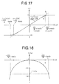
- the input/output characteristics of the second prior art is illustrated in Fig. 17, and the non-linearity E defined by the following equation (18) is illustrated in Fig. 18.
- the absolute value of the non-linearity E is increased according to increasing of the differential output current ⁇ I associated with increasing of the differential input voltage ⁇ V. This is caused due to I D -V GS characteristics of the MOSFET, in which a drain current I n does not vary in proportion to variation of a gate-source voltage V GS . In other words, as expressed in the equation (14), this is caused due to the fact that the differential input voltage ⁇ V and the voltage V R at opposite ends of the source resistor (accordingly, the differential output current ⁇ I) are not proportional to each other.
- Fig. 19 shows a circuit construction of the differential voltage-to-current converter circuit disclosed in Japanese Unexamined Patent Publication No. 57-46161 (hereinafter referred to as "third prior art). As shown in Fig. 19, the third prior art is designed for eliminating non-linearity of an amplifier element by combination of a differential amplifier and bipolar current-mirror circuit having two outputs.
- the relationship between the differential output current ⁇ I and the differential input voltage ⁇ V can be expressed by the following equation (21).
- the input/output characteristics is shown in Fig. 20.
- the non-linearity E (expressed by the following equation (22)) of the differential voltage-to-current converter circuit of the third prior art is illustrated in Fig. 21. From Fig. 21, the non-linearity E becomes 0 in a range of the differential input voltage ⁇ V being ⁇ RI0/3. Therefore, a linearity can be improved.
- the range of the differential current, in which the non-linearity can be reduced is in a range of 1/3 of the constant current I0. Accordingly, in order to obtain the output comparable with those in the prior arts 1 and 2, the constant current has to be three time grater, or, in the alternative, a size ratio between the bipolar transistors forming the mirror-current circuit has to be selected appropriately.
- the construction of the differential amplifier disclosed in Japanese Unexamined Utility Model Publication No. 63-44521 hereinafter referred to as "fourth prior art
- the input/output characteristics of the fourth prior art is illustrated.
- Figs. 24 and 25 show a circuit construction of a differential amplifier disclosed in Japanese Unexamined Patent Publication No. 59-229909 (hereinafter referred to as "fifth prior art").
- the differential amplifier of the fifth prior art is constructed by contacting the drain of a first FET forming a differential pair to a load, the drain of a second FET forming the differential pair to the source of a third FET, and the gate of the third FET to a junction between the drain and the load of the first FET, and the drain of the third FET to the load.
- g m1 g m2
- the condition defined in the equation (23) with respect to the differential amplifier of the fifth prior art can be only satisfied by a fine signal alternating operation near a certain direct current operation point of the circuit (in the case where amplitude of the voltage at respective points in the circuit is small).
- the third prior art is capable of reducing non-linearity of the differential amplifier circuit by combination of the differential amplifier circuit and the current-mirror circuit with two outputs employing the bipolar process.
- a new circuit is required for taking the current out.
- the amplitude of the differential output current is merely 1/3 of the current value I0 of the constant current source at the greatest.
- the currents flowing through the transistor of the bipolar current-mirror circuit and the differential MOSFET influence each other.
- an Early voltage V A of the bipolar transistor is typically smaller than the Early voltage V A of the MOS transistor
- the variation magnitude of the collector currents of the transistors Q1 and Q2 and the drain current of N1 and N2 in Fig. 19 becomes greater than that in the case where MOS transistors are employed as all transistors. Therefore, it becomes difficult to design the size and so forth of the transistor independently.
- the third prior art comprises the MOS transistors and the bipolar transistors.
- MOS transistors For fabricating these different types of transistors on the common semi conductor chip, production process is inherently increased to cause rising of the production cost.
- the condition expressed by the equation (23) is only satisfied by a fine signal alternating operation near a certain direct current operation point of the circuit (in the case where amplitude of the voltage at respective points in the circuit is small) and cannot be satisfied when amplitude of the voltage is large.
- Another object of the invention is to provide a MOS differential voltage-to-current converter circuit, in which a mutual conductance is determined only by the resistance value 2R0 or (R01 + R02 ) between source (or drain) terminals of the differential pair MOSFET.
- a MOS differential voltage-to-current converter circuit comprises: first and second MOS transistors; a resistor connected between the sources of the first and second MOS transistors; a first constant current source for supplying operation current for the first and second MOS transistors; third and fourth MOS transistors having sources respectively connected to the source of the first and second MOS transistors and receiving a differential input voltage at the gates thereof; second and third constant current sources for supplying operation currents for the third and fourth MOS transistors; and first and second signal transmission means for transmitting drain outputs of the third and fourth MOS transistors to the gates of the first and second MOS transistors for taking the current flowing through the first and second MOS transistors as a differential output.
- a MOS differential voltage-to-current converter circuit comprising: first and second MOS transistors; a resistor connected between the sources of the first and second MOS transistors; a first constant current source for supplying operation current for the first and second MOS transistors; third and fourth MOS transistors having sources respectively connected to the source of the first and second MOS transistors and receiving a differential input voltage at the gates thereof; a first differential amplifier circuit receiving a gate input and a drain output of the third MOS transistor as inputs and applying an output as the differential output to the gate of the first MOS transistor; and a second differential amplifier circuit receiving a fate input and a drain output of the fourth MOS transistor as inputs and applying an output as the differential output to the gate of the second MOS transistor for taking the current flowing through the first and second MOS transistors as a differential output.
- a MOS differential voltage-to-current converter circuit comprises: first and second MOS transistors; a resistor connected between the drains of the first and second MOS transistors; a first constant current source for supplying operation current for the first and second MOS transistors; third and fourth MOS transistors having sources respectively connected to the drain of the first and second MOS transistors and receiving a differential input voltage at the gates thereof; second and third constant current sources for supplying operation currents for the third and fourth MOS transistors; and first and second signal transmission means for transmitting drain outputs of the third and fourth MOS transistors to the gates of the first and second MOS transistors for taking the current flowing through the first and second MOS transistors as a differential output.
- a MOS differential voltage-to-current converter circuit comprises: first and second MOS transistors; a resistor connected between the drains of the first and second MOS transistors; a first constant current source for supplying operation current for the first and second MOS transistors; third and fourth MOS transistors having sources respectively connected to the drains of the first and second MOS transistors and receiving a differential input voltage at the gates thereof; a first differential amplifier circuit receiving a gate input and a drain output of the third MOS transistor as inputs and applying an output as the differential output to the gate of the first MOS transistor; and a second differential amplifier circuit receiving a gate input and a drain output of the fourth MOS transistor as inputs and applying an output as the differential output to the gate of the second MOS transistor for taking the current flowing through the first and second MOS transistors as a differential output.
- a MOS differential voltage-to-current converter circuit comprises: first and second MOS transistors; a resistor connected between the drains of the first and second MOS transistors; a first constant current source for supplying operation current for the first and second MOS transistors; third and fourth MOS transistors having sources respectively connected to the drains of the first and second MOS transistors and receiving a differential input voltage at the gates thereof; a first current-mirror circuit receiving the drain output of the third MOS transistor as a current input and having a current output terminal connected to the gate of the first MOS transistor; and a second current-mirror circuit receiving the drain output of the fourth MOS transistor as a current input and having a current output terminal connected to the gate of the second MOS transistor for taking the current flowing through the first and second MOS transistors as a differential output.
- the first and second signal transmission means may comprise one of an amplifier circuit, an attenuation circuit and a voltage follower circuit.
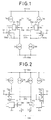
- Figs. 1 to 4 show a circuit construction of the first embodiment of the MOS differential voltage-to-current converter circuit of the present invention, and an input/output characteristics thereof.
- first and second MOSFETs (N1 and N2 or P1 and P2) forming a differential pair in this embodiment are connected to first and second constant current sources I01 and I02. Between the source terminals of the first and second MOSFETs, one source resistor 2R0 is connected.
- Fig. 1 shows the circuit construction of a sink type MOS differential voltage-to-current converter circuit
- Fig. 2 shows the circuit construction of a source type MOS differential voltage-to-current converter circuit.
- FIGs. 1 and 2 the circuit elements performing substantially the same functions to those in the first prior art illustrated in Fig. 13 will be represented by the same reference numerals.
- N3 and N4 of Figs. 1 and 2 denote third and fourth NMOSFETs, and
- A1 and A2 denote first and second signal transmission circuits.
- circuit constructions illustrated in Figs. 26 and 27 can be employed on the other hand, as the signal transmission circuits A1 and A2 in Fig. 2, the circuit illustrated in Fig. 27 may be employed.
- the constant current source of Fig. various current-mirror circuits illustrated in Figs. 30 to 33 may be employed.
- the third and fourth constant current sources I03 and I04 are connected to the drain terminals of MOSFET N3 and N4, respectively for maintaining the gate-source terminal voltages V GS3 and V GS4 of N3 and N4 constant.
- the source terminals of N3 and N4 are respectively connected to the source terminals of N1 and N2 to maintain the voltage between the first input terminal V1 and the source terminal of N1 and the voltage between the second input terminal V2 and the source terminal of N2 constant.
- the drain terminals of N3 and N4 are respectively connected to the gate terminals of N1 and N2.
- V R The voltage at opposite ends of the source resistor 2R0 is expressed by ⁇ V R .
- V T3 and V T4 are threshold voltages of N3 and N4.
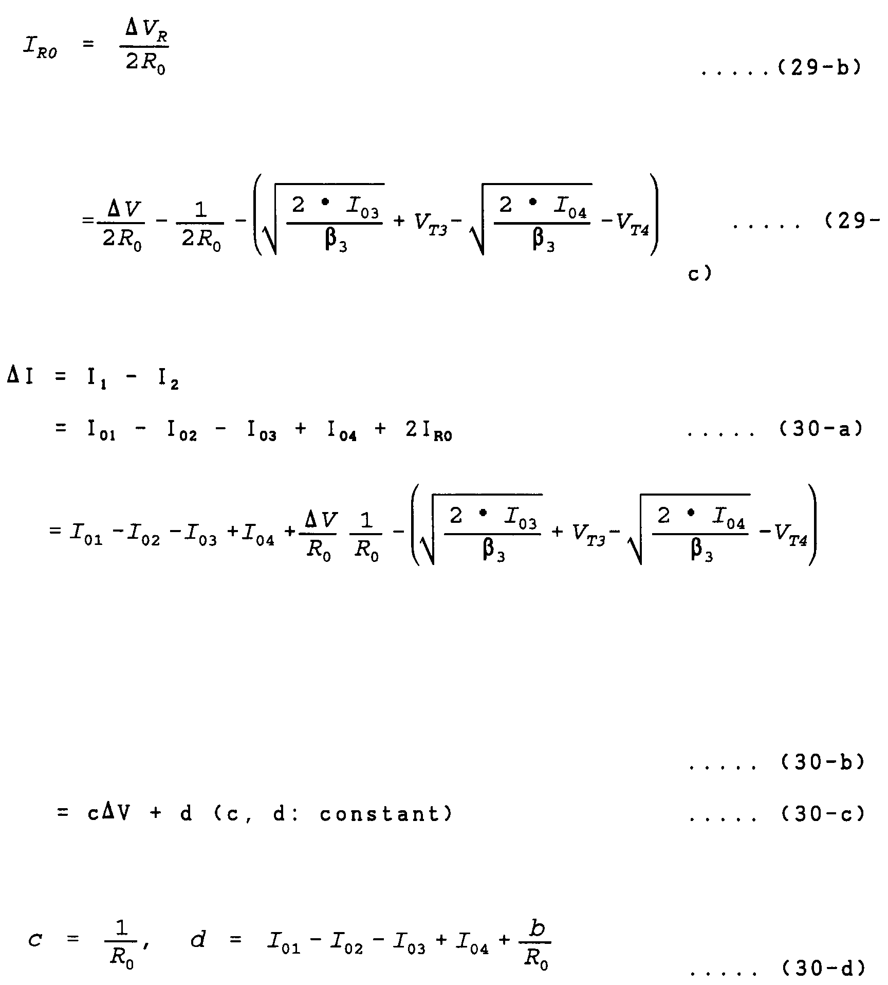
- the equation (29-a) can be established from the Kirchhoff's law with respect to the opposite ends of the resistor 2R0. Form this. the differential output current ⁇ I can be expressed by the equation (30-a).
- I R0 With respect to the voltage ⁇ V R at opposite ends of the resistor 2R0, I R0 can be derived from the equation (29-b).
- the equation (28-b) is employed as ⁇ V R
- the equation (29-c) can be established.
- the differential output current ⁇ I can be expressed by the equation (30-b).
- the differential output current ⁇ I is in a linear relationship with the differential input voltage ⁇ V.
- This relationship can be expressed by the equation (30-c).
- constants c and d are respectively derived from the equation (30-d) and the constant b represents (-V GS3 + V GS4 ) similarly to (28-d).
- the constant c represents the mutual conductance and the constant d is an offset current.
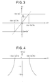
- Fig. 3 shows the input/output characteristics of the shown embodiment of the differential voltage-to-current converter circuit and Fig. 4 shows the characteristics of the non-linearity E in relation to the differential input voltage ⁇ V.
- Each of the source terminals of N3 and N4 which are connected to the constant current sources I03 and I04 at the drain terminals for maintaining the gate-source terminal voltages V GS3 and V GS4 constant, is connected to the source terminal of each of N1 and N2 as the differential pair so that the voltage between the first input terminal V1 and the source terminal of N1 and the voltage between the second input terminal V2 and the source terminal of N2 are constant.
- the signal transmission circuit A1 and A2 respectively comprise differential amplifier circuits .
- the first and second input terminals V1 and V2 are connected.
- the drain terminals of N3 and N4 are connected.
- Outputs of the differential amplifier circuits A1 and A2 are connected to the gate terminals of the first and second NMOSFETs N1 and N2, respectively.
- the input/output characteristics, mutual conductance and non-linearity of the differential voltage-to-current converter circuit employing the differential amplifiers A1 and A2 as the first and second signal transmission circuits, can be derived in the similar manner to the case of the foregoing embodiment with direct connection.
- the differential amplifier circuits A1 and A2 operate to maintain the gate-source terminal voltages V GS3 and V GS4 of N3 and N4. Namely, they compensate following up of the source terminals of N3 and N4 to the first and second input terminals and whereby stabilize the operation of the differential voltage-to-current converter circuit. If the amplification factors of the differential amplifier circuits A1 and A2 are sufficiently high, V GS3 and V GS4 can be maintained constant. Then, the mutual conductance g m and the non-linearity E can be expressed by the equations (33-b) and (34-b).
- differential amplifier circuits of Fig. 27 are employed as the signal transmission circuits A1 and A2 of the differential voltage-to-current converter circuit shown in Fig. 2.
- non-inverting inputs of the differential amplifier circuits A1 and A2 are connected to first and second input terminals V1 and V2, respectively.
- the inverting inputs are connected to the drain terminals of N3 and N4.
- the outputs of the differential amplifier circuits A1 and A2 are connected to gate terminals of first and second PMOSFETs P1 and P2.
- the drain voltage of N3 is lowered (the drain voltage of N4 is risen) .
- the output of the differential amplifier circuit A1 is risen and the output of the differential amplifier circuit A2 is lowered.
- These outputs are applied to respective gate terminals of P1 and P2 of the differential pair. Therefore, the drain current of P1 is decreased and the drain current of P2 is increased. Then, the difference of the drain currents of P1 and P2 flows through the source resistor 2R0.
- the differential amplifier circuits A1 and A2 operate to maintain the gate-source terminal voltages V GS3 and V GS4 of N3 and N4.
- the input/output characteristics and the non-linearity of the differential voltage-to-current converter circuit may be derived in the similar manner even when the inputs of the first and second signal transmission circuits A1 and A2 are first and second input terminals.
- Figs. 5 ⁇ 8 show the circuit construction, input/output characteristics of the second embodiment of the MOS differential voltage-to-current converter circuit according to the present invention.
- respective source terminals of first and second MOSFETs (N1 and N2 or P1 and P2) forming a differential pair in this embodiment are connected to one terminals of first and second resistors R01 and R02.
- the other terminals of the first and second source resistors R01 and R02 are commonly connected.
- To the junction of common connection of the first and second resistors R01 and R02 is connected to a constant current source I0.
- Fig. 5 shows the circuit construction of a sink type MOS differential voltage-to-current converter circuit
- Fig. 6 shows the circuit construction of a source type MOS differential voltage-to-current converter circuit.
- the functionally common elements to those in Fig. 16 which illustrates the second prior art will be represented by the same reference numerals.
- N3 and N4 are third and fourth NMOSFETs
- V B3 and V B4 are backgate terminals and voltages.
- circuit constructions illustrated in Figs. 26 and 27 can be employed on the other hand, as the signal transmission circuits A1 and A2 in Fig. 6, the circuit illustrated in Fig. 27 may be employed.
- the constant current sources of Figs. 5 and 6 various current-mirror circuits illustrated in Figs. 30 to 33 may be employed.
- the constant current sources I03 and I04 are connected to the drain terminals of MOSFET N3 and N4, respectively for maintaining the gate-source terminal voltages V GS3 and V GS4 of N3 and N4 constant.
- the source terminals of N3 and N4 are respectively connected to the source terminals of N1 and N2 to maintain the voltage between the first input terminal V1 and the source terminal of N1 and the voltage between the second input terminal V2 and the source terminal of N2 constant.
- the drain terminals of N3 and N4 are respectively connected to the gate terminals of N1 and N2.
- the equation (39) is established on the basis of Kirchhoff's law with respect to the common junction
- the voltage ⁇ V R at opposite ends of the resistors R01 and R02 is expressed by the equation (40)
- the currents I R01 and I R02 can be expressed by the equation (41).
- the differential output current ⁇ I is expressed by the equation (42-a).
- Equation (42-d) a linear relational expression of the differential output current ⁇ I and the differential input voltage ⁇ V can be derived (equation (42-d). It should be noted that constants c and d are defined by equations (42-e) and (42-f).
- I0 I R01 + I R02 ,
- I R01 I1 + I03,
- I R02 I2 + I04 (39)
- R01 I R01 - R02 I R02 ⁇ V R (40)
- the mutual conductance g m , non-linearity E and the range to be established are defined by the equations (46) to (48).
- the characteristic curve of the non-linearity E is illustrated in Fig. 8.
- the non-inverting inputs of the differential amplifier circuits A1 and A2 are connected to first and second input terminals V1 and V2, respectively.
- the inverting inputs are connected to the drain terminals of N3 and N4.
- the outputs of the differential amplifier circuits A1 and A2 are connected to gate terminals of first and second NMOSFETs N1 and N2.
- the input/output characteristics and the non-linearity E can be derived in the similar manner to the foregoing first embodiment. Also, the operation is as set forth above, the differential amplifier circuits A1 and A2 operate to maintain the gate-source terminal voltages V GS3 and V GS4 of N3 and N4. Namely, they compensate following up of the source terminals of N3 and N4 to the first and second input terminals and whereby stabilize the operation of the differential voltage-to-current converter circuit.
- the mutual conductance g m and the non-linearity E are defined by the equations (46-b) and (47-b).
- the non-inverting inputs of the differential amplifier circuits A1 and A2 are connected to first and second input terminals V1 and V2, respectively.
- the inverting inputs are connected to the drain terminals of N3 and N4.
- the outputs of the differential amplifier circuits A1 and A2 are connected to gate terminals of first and second PMOSFETs P1 and P2.
- the differential amplifier circuits A1 and A2 operate to maintain the gate-source terminal voltages V GS3 and V GS4 of N3 and N4. Namely, they compensate following up of the source terminals of N3 and N4 to the first and second input terminals and whereby stabilize the operation of the differential voltage-to-current converter circuit.
- the mutual conductance g m and the non-linearity E are defined by the equations (46-b) and (47-b).
- Figs. 9 and 10 shows the third embodiment of the differential voltage-to-current converter circuit of the present invention.
- Fig. 9 shows the differential voltage-to-current circuit which is constructed by replacing NMOSFETs N1 and N2 in the differential voltage-to-current converter circuit of Fig. 1 with PMOSFETs P1 and P2.
- Fig. 10 shows the embodiment, in which the PMOSFETs P1 and P2 of Fig. 2 with NMOSFETs N1 and N2.
- the resistor 2R0 is connected between the drain terminals of P1 and P2 or N1 and N2 of the differential pair,
- like circuit elements to those of Figs. 1 and 2 will be represented by the same reference numerals.
- Fig. 9 shows the circuit construction of a sink type MOS differential voltage-to-current converter circuit and Fig. 10 shows the circuit construction of a source type MOS differential voltage-to-current converter circuit.
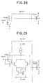
- circuit constructions illustrated in Figs. 28 and 29 can be employed on the other hand, as the signal transmission circuits A1 and A2 in Fig. 10, the circuit illustrated in Fig. 28 may be employed.
- the constant current source various current-mirror circuits illustrated in Figs. 30 to 33 may be employed.
- the input/output characteristics and the non-linearity E of the shown embodiment can be derived in the similar manner to the first embodiment. Thus, equivalent characteristics to the first embodiment can be obtained.
- Figs. 11 and 12 shows the third embodiment of the differential voltage-to-current converter circuit of the present invention.
- Fig. 9 shows the differential voltage-to-current circuit which is constructed by replacing NMOSFETs N1 and N2 in the differential voltage-to-current converter circuit of Fig. 1 with PMOSFETs P1 and P2.
- Fig. 10 shows the embodiment, in which the PMOSFETs P1 and P2 of Fig. 2 with NMOSFETs N1 and N2.
- the first and second resistors R01 and R02 are connected between the drain terminals of P1 and P2 or N1 and N2 of the differential pair,
- like circuit elements to those of Figs. 5 and 6 will be represented by the same reference numerals.
- Fig. 11 shows the circuit construction of a sink type MOS differential voltage-to-current converter circuit
- Fig. 12 shows the circuit construction of a source type MOS differential voltage-to-current converter circuit.
- circuit constructions illustrated in Figs. 28 and 29 can be employed on the other hand, as the signal transmission circuits A1 and A2 in Fig. 12, the circuit illustrated in Fig. 29 may be employed.
- the constant current source various current-mirror circuits illustrated in Figs. 30 to 33 may be employed.
- the input/output characteristics and the non-linearity E of the shown embodiment can be derived in the similar manner to the second embodiment. Thus, equivalent characteristics to the first embodiment can be obtained.
- the first and second signal transmission circuits A1 and A2 in the foregoing first to fourth embodiments of the invention may be constructed by source followers, voltage followers having amplification factor being 1 or so forth, in addition to the differential amplifiers and direct connection.
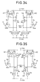
- the shown embodiment (Figs. 34 and 35) of the differential voltage-to-current converter circuit is constructed by connecting the first and second constant current sources I01 and I02 to the first and second MOSFETs (N1 and N2 or P1 and P2).
- One resistor 2R0 is connected between the source terminals of the first and second MOSFETs.
- Fig. 34 shows the circuit construction of a sink type MOS differential voltage-to-current converter circuit
- Fig. 35 shows the circuit construction of a source type MOS differential voltage-to-current converter circuit.
- the source terminals of the third and fourth MOSFETs are connected to the source terminals of the first and second MOSFETs.
- the drain terminals of the third and fourth MOSFETs are connected to respective input sides of the first and second current mirror circuits M1 and M2.
- the output terminals of the first and second current-mirror circuits M1 and M2 are connected to the third and fourth constant current sources and gate terminals of the first and second MOSFETs.
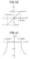
- Figs. 38 to 41 show the circuit construction, and input/output characteristics of the sixth embodiment of the differential voltage-to-current converter circuit according to the present invention.
- the shown embodiment of the differential voltage-to-current converter circuit is constructed by connecting one terminals of the first and second resistors R01 and R02 to the source terminals of the first and second MOSFETs (N1 and N2 or P1 and P2). The other terminals of the first and second resistors R01 and R02 are connected in common.
- the constant current source I0 is connected to the junction of the common connection between the first and second resistors R01 and R02.
- Fig. 38 shows the circuit construction of a sink type MOS differential voltage-to-current converter circuit
- Fig. 39 shows the circuit construction of a source type MOS differential voltage-to-current converter circuit.
- respective signs in Figs. 38 and 39 have the same meaning to the corresponding signs in Fig. 16 which illustrates the second prior art.
- N3 and N4 represent third and fourth NMOSFETs.
- the constant current source can be constructed as shown in Figs. 30, 31, 32 and 33.
- the source terminals of the third and fourth MOSFETs are connected to the source terminals of the first and second MOSFETs.
- the drain terminals of the third and fourth MOSFETs are connected to respective input sides of the first and second current mirror circuits M1 and M2.
- the output terminals of the first and second current-mirror circuits M1 and M2 are connected to the third and fourth constant current sources and the gate terminals of the first and second MOSFETs. Accordingly, when the input V1 is risen for example, the gate-source terminal voltage V GS3 is temporarily increased. Associating therewith, the drain current of N3 and the input current of M1 are also risen.
- the MOS differential voltage-to-current converter circuit establishes the negative feedback with the shown construction, in which the source (drain) resistors are provided, the source (drain terminals of the first and second MOSFETs are connected to the source terminals of the third and fourth MOSFETs, the drain terminals of the third and fourth MOSFETs are respectively connected to the input sides of the first and second current mirror circuits M1 and M2, and the outputs of the current-mirror circuits M1 and M2 are connected to the constant current source and the gate terminals of the first and second MOSFETs.
- the gate voltage of N1 and N2 are converged at the voltage where the current I03 flowing through N3 and the current I04 flowing through N4 are equal to each other so that V1, the voltage V GS3 between the source terminal of the N1 and the voltage V GS4 between V2 and the voltage V2 and the source terminal of N4 become constant.
- the first and second signal transmission means which has the inputs connected to the respective of the first and second input terminals and/or to the drain terminals of the third and fourth MOSFETs, and the outputs connected to respective gate terminals of the first and second MOSFETs.
- the mutual conductance g m of the differential voltage-to-current converter circuit can be determined only by the resistance value 2R0, R01 + R02 between the source (drain) terminals. Also, even when the differential output current is increased associating with increasing of the differential input voltage, the non-linearity E can be held 0.
- the differential current-to-voltage converter circuit it becomes possible to avoid increasing of non-linearity due to influence of various property of the differential MOSFET (such as, non-linearity of I D -V GS characteristics, fluctuation of the gain coefficient ⁇ , variation of the threshold voltage V T due to backgate effect, saturation of MOS due to end channel effect and so forth, variation of the I D -V DS characteristics within the non-saturated range and so forth) , within a predetermined range of the differential input voltage.
- various property of the differential MOSFET such as, non-linearity of I D -V GS characteristics, fluctuation of the gain coefficient ⁇ , variation of the threshold voltage V T due to backgate effect, saturation of MOS due to end channel effect and so forth, variation of the I D -V DS characteristics within the non-saturated range and so forth
- Characteristics variation factor of the MOSFET is quite large in comparison with that of the bipolar transistor and is specific to the MOSFET. Conventionally, such characteristics variation was inevitable in the MOSFET circuit. According to the present invention, even when the circuit elements located at symmetric positions on the circuit diagram do not have the same characteristics, the relationship between the differential input voltage ⁇ V and the voltage ⁇ V R at opposite ends of the source (drain) resistor and the relationship between the differential input voltage ⁇ V and the differential output current ⁇ I can be maintained linear without depending upon the characteristics variation of the MOSFETs. Therefore, the linearity of the differential voltage-to-current converter can be significantly improved.
- the differential voltage-to-current converter circuit can be fabricated through a MOS process, which can simply the fabrication process contributing lowering of the production cost.
Landscapes
- Engineering & Computer Science (AREA)
- Power Engineering (AREA)
- Physics & Mathematics (AREA)
- Nonlinear Science (AREA)
- Amplifiers (AREA)
Abstract
Description
- The present invention relates to a MOS voltage-to-current converter circuit employing a field-effect MOS transistor formed on a semiconductor integrated circuit chip. More specifically, the invention relates to a MOS differential voltage-to-current converter circuit which suppresses fluctuation of a mutual conductance.
- Construction and operation of the conventional MOS differential voltage-to-current converter circuit will be discussed with reference to the drawings. Throughout the disclosure, a field-effect MOS transistor will be simply referred to as "MOSFET", N-channel field - effect MOS transistor will be referred to as "NMOSFET", and similarly, P-channel field-effect MOS transistor will be referred to as "PMOSFET".
- Concerning the reference signs to be used in the following disclosure, I, I*, I**, ΔI represent current, V, V*, V**, ΔV represent voltage, R, R*, R** represent resistance, β, β* represent gain coefficient of MOSFET, and gm, gm* represent mutual conductance of the differential voltage-to-current converter circuit. *,** represent numerals.
- One example of the circuit construction of the conventional differential voltage-to-current converter circuit (hereinafter referred to as "first prior art") is illustrated in Fig. 13. In Fig. 13, N₁ and N₂ represent first and second NMOSFET, 2R₀ represents one source resistance (resistance value 2R₀) mutually connecting the source terminals of N₁ and N₂. V₁ and V₂ represent first and second input voltages of the differential voltage-to-current converter circuit, VB1 and VB2 represent backgate voltages On the other hand, I₀₁ and I₀₂ represent first and second constant current sources, respectively. I₁ and I₂ represent first and second output currents of the differential voltage-current converter circuit, respectively.
- Here, it is assumed that currents I₀₁ and I₀₂ of the first and second constant current sources are equal to each other. Double of the current I₀₁ or I₀₂ is defined as a constant current I₀₀ which is expressed by the following equation (1). A differential output current ΔI and a differential input voltage ΔV are respectively expressed by the following equation (2).
- Discussion is now given for an input/output characteristics of the differential input voltage ΔV and the differential output current ΔI in the differential voltage-to-current converter circuit of Fig. 13. Assuming the gain coefficient of the MOSFET is β ,a drain current I₀ is expressed by the following equation (3) in the saturated range. It should be noted that, in the equation (3), VGS represents a gate-source voltage, VT represents a threshold voltage. Accordingly, VGS can be expressed by the following equation (4).
- Applying Kirchhoff's law in the loops of V₁ ∼ VGS1 ∼ V2R0 ∼ VGS2 ∼ V₂, the following equation (5) can be established. Then, the differential input voltage ΔV can be expressed by the following equation (6) with taking the current flowing through a resistor 2R₀ between the sources being IR0. It should be appreciated that, the gain coefficients β of N₁ and N₂ forming a differential pair in the equation (6) are mutually equal.
- From Kirchhoff's law, the following equation (7-a) can be established with respect to both ends of the resistor 2R₀. Therefore, the current IR0. flowing through the source resistor 2R₀ is expressed by the following equation (7-b). Therefore, first and second output currents I₁ and I₂ are expressed by the following equation (7-c). Substituting the equation (6) with these, the following equation (8) expressing the input/output characteristics of the differential input voltage ΔV and the differential output current ΔI can be derived.
- The input/output characteristics (curve a in the drawing) of the differential voltage-to-current converter circuit of the first prior art, which characteristics is expressed by the equation (8), is illustrated in Fig. 14. A reciprocal of the mutual conductance gm of the differential voltage-to-current converter circuit can be obtained by differentiating ΔV with the differential output current ΔI , and expressed by the following equation (9) . As shown in Fig. 14, the mutual conductance gm becomes the maximum value gmmax when the differential input voltage ΔV is 0. At this time, from the equation (8), ΔI becomes 0, the reciprocal of the maximum value gmmax is expressed by the following equation (10). It should be appreciated that the maximum value gmmax of the mutual conductance corresponds to the gradient of a tangent b of the input/output characteristics curve a of Fig. 14 at ΔV = 0, the tangent b is expressed by:

A coefficient E expressing non-linearity of the input/output characteristics of the differential voltage-to-current converter circuit is defined by the equation (12-a). Namely, the non-linearity E can be obtained by obtaining a difference between the input/output characteristics curve a and the tangent b with respect to ΔV and by dividing the difference by the value (gmmax x ΔV) of the tangent b. - Expressing the a rate of I₀₀ as double of the current of the first and second current source and the differential output current ΔI as a coefficient α (equation (11)), the non-linearity E can be expressed with the coefficient α and I₀₀ in the following equation (12-b). A curve in Fig. 15 is a plot of the non-linearity with respect to the differential input voltage ΔV (horizontal axis).
- Respective values shown in Figs. 14 and 15 are derived with taking the constant current I₀₀ = 1 (mA), gain coefficient





wherein


From Figs. 14 and 15, it should be appreciated that the absolute value of the non-linearity E is increased according to increasing of the differential output current ΔI associated with increasing of the differential input voltage ΔV. This is caused due to ID-VGS characteristics of the MOSFET, in which a drain current In does not vary in proportion to variation of a gate-source voltage VGS. In other words, as expressed in the equation (8), this is caused due to the fact that the differential input voltage ΔV and the voltage V2R0 at opposite ends of the source resistor (accordingly, the differential output current ΔI) are not proportional to each other. - The characteristics of the above-mentioned differential voltage-to-current converter circuit is similarly applicable for the case where the first and second NMOSFETs are replaced with PMOSFETs.
- Figs. 16 shows another example of a circuit construction of the conventional the differential voltage-to-current converter circuit in which first and second resistors R₀₁ and R₀₂ are connected in common (hereinafter referred to as "second prior art"). As shown in Fig. 16, the second prior art is constructed by connecting first and second resistors R₀₁ and R₀₂ to source terminals of first and second MOSFETs N₁ and N₂ at each one end, and connecting one constant current source I₀ to a common junction of the first and second resistors R₀₁ and R₀₂. V₁ and V₂ denote first and second inputs voltages, VB1 and VB2 denote a backgate terminal voltages, and I₁ and I₂ denote the first and second output currents.
- The resistance values of the first and second resistors R₀₁ and R₀₂ are assumed to be equal to each other . Then, the source resistor R₀₀ is defined as expressed in the following equation (13-a). Also, the differential output current ΔI is defined to be expressed by the following equation (13-b).
- The differential input voltage ΔV in the differential voltage-to-current converter circuit of Fig. 16 is derived in the similar manner to the foregoing first prior art by replacing the source resistor 2R₀ with 2R₀₀ and IO0 in the equation (1) with I₀, and thus expressed by the following equation (14). The input/output characteristics of the second prior art is illustrated in Fig. 17, and the non-linearity E defined by the following equation (18) is illustrated in Fig. 18.


wherein


Respective values in Figs. 17 and 18 are derived with assumption of constant current source I₀ = 1 (mA) , gain coefficient

- From Figs. 17 and 18, it should be appreciated that the absolute value of the non-linearity E is increased according to increasing of the differential output current ΔI associated with increasing of the differential input voltage ΔV. This is caused due to ID-VGS characteristics of the MOSFET, in which a drain current In does not vary in proportion to variation of a gate-source voltage VGS. In other words, as expressed in the equation (14), this is caused due to the fact that the differential input voltage ΔV and the voltage VR at opposite ends of the source resistor (accordingly, the differential output current ΔI) are not proportional to each other.
- The characteristics of the above-mentioned the differential voltage-to-current converter circuit is similarly applicable for the case where the first and second NMOSFETs are replaced with PMOSFETs.
- Fig. 19 shows a circuit construction of the differential voltage-to-current converter circuit disclosed in Japanese Unexamined Patent Publication No. 57-46161 (hereinafter referred to as "third prior art). As shown in Fig. 19, the third prior art is designed for eliminating non-linearity of an amplifier element by combination of a differential amplifier and bipolar current-mirror circuit having two outputs.
- In the third prior art, assuming the current-mirror circuit and the constant current source are both ideal, the relationship between the differential output current ΔI and the differential input voltage ΔV can be expressed by the following equation (21). The input/output characteristics is shown in Fig. 20. The non-linearity E (expressed by the following equation (22)) of the differential voltage-to-current converter circuit of the third prior art is illustrated in Fig. 21. From Fig. 21, the non-linearity E becomes 0 in a range of the differential input voltage ΔV being ±RI₀/3. Therefore, a linearity can be improved.
- However , in the third prior art, in order to take the current out, it becomes necessary to add new circuit, such as an output side transistor added for the bipolar current-mirror circuit. These circuit varies signals in non-linear fashion according to variation of the input current. Therefore, the non-linearity of the voltage-to-current converter circuit is increased beyond 0 in the equation (22) to degrade effect in improvement of the linearity.
- As shown in Figs. 20, 21, with the circuit construction in the third prior art, the range of the differential current, in which the non-linearity can be reduced, is in a range of 1/3 of the constant current I₀. Accordingly, in order to obtain the output comparable with those in the
prior arts




wherein

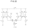
In Fig. 22, the construction of the differential amplifier disclosed in Japanese Unexamined Utility Model Publication No. 63-44521 (hereinafter referred to as "fourth prior art") In Fig. 23, the input/output characteristics of the fourth prior art is illustrated. - In the fourth prior art, for respective first and second bipolar transistors, third and fourth bipolar transistors, bases and emitters of which are mutually connected, are employed. By applying the constant current to this, the linearity of the differential amplifier circuit is improved in the range of ±αIEE of the output current.
- As shown in Fig. 22, in the circuit construction of the fourth prior art, direct current is constantly applied to input signal sources V₁ and V₂ from emitters of fifth and sixth transistors Q₄ and Q₆. Therefore, the input signal sources V₁ and V₂ are required drive performance for supplying the supplied current.
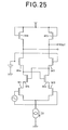
- Figs. 24 and 25 show a circuit construction of a differential amplifier disclosed in Japanese Unexamined Patent Publication No. 59-229909 (hereinafter referred to as "fifth prior art"). As shown, the differential amplifier of the fifth prior art is constructed by contacting the drain of a first FET forming a differential pair to a load, the drain of a second FET forming the differential pair to the source of a third FET, and the gate of the third FET to a junction between the drain and the load of the first FET, and the drain of the third FET to the load.
- In the fifth prior art, the relationship between the input voltage and the output voltage of the differential amplifier in the range where the mutual conductance gm1 to gm4 of the FETs (M1 to M4) satisfy the condition expressed in the following equation (23), becomes as expressed in the following equation (24). Then, the linearity of the input/output characteristics can be improved.


The condition defined in the equation (23) with respect to the differential amplifier of the fifth prior art can be only satisfied by a fine signal alternating operation near a certain direct current operation point of the circuit (in the case where amplitude of the voltage at respective points in the circuit is small). - In the MOS differential voltage-to-current converter circuit in the foregoing first, second and fifth prior arts, a problem in degradation of the linearity of the input/output characteristics according to increasing of the differential output current ΔI associated with increasing of the differential input voltage ΔV and narrowing of a dynamic range, is encountered. There is further encountered a problem in increasing of non-linearity due to influence of variation of the properties of MOSFET, such as non-linearity of ID -VGS characteristics, fluctuation of gain coefficient β, variation of a threshold voltage VT due to a backgate effect, variation of ID-IGS characteristics up to MOS saturation range due to short channel effect and so forth.
- The third prior art is capable of reducing non-linearity of the differential amplifier circuit by combination of the differential amplifier circuit and the current-mirror circuit with two outputs employing the bipolar process. However, a new circuit is required for taking the current out. Also, the amplitude of the differential output current is merely 1/3 of the current value I₀ of the constant current source at the greatest.
- Accordingly, in the third prior art, it becomes necessary to provide the constant current I₀ three times greater in order to obtain comparable output to the first and second prior arts, or to appropriately adjust the size ratio of the bipolar transistors forming the current-mirror circuit. Therefore, there is encountered a problem in difficulty in reducing consumed current in the circuit construction of the third prior art.
- On the other hand, in the circuit construction of the third prior art, the currents flowing through the transistor of the bipolar current-mirror circuit and the differential MOSFET influence each other. For instance, since an Early voltage VA of the bipolar transistor is typically smaller than the Early voltage VA of the MOS transistor, the variation magnitude of the collector currents of the transistors Q₁ and Q₂ and the drain current of N₁ and N₂ in Fig. 19 becomes greater than that in the case where MOS transistors are employed as all transistors. Therefore, it becomes difficult to design the size and so forth of the transistor independently.
- Furthermore, the third prior art comprises the MOS transistors and the bipolar transistors. For fabricating these different types of transistors on the common semi conductor chip, production process is inherently increased to cause rising of the production cost.
- Next, in the circuit construction of the foregoing fourth prior art, it is required the direct current constantly flowing into the input signal source and thus is required a driving performance to supply the current to the input signal source. Also, the performance of the whole circuit is significantly influenced by the external circuit (power source). Therefore, this circuit encounters a problem in difficulty of handling.
- In the differential amplifier of the fifth prior art, the condition expressed by the equation (23) is only satisfied by a fine signal alternating operation near a certain direct current operation point of the circuit (in the case where amplitude of the voltage at respective points in the circuit is small) and cannot be satisfied when amplitude of the voltage is large.
- Therefore, it is an object of the present invention to provide a MOS differential voltage-to-current converter circuit which can improve linearity by avoiding increasing of non-linearity due to various property of MOSFETs of a differential pair in a range of predetermined differential input voltage.
- Another object of the invention is to provide a MOS differential voltage-to-current converter circuit, in which a mutual conductance is determined only by the resistance value 2R₀ or (R₀₁ + R₀₂) between source (or drain) terminals of the differential pair MOSFET.
- According to the first aspect of the invention, a MOS differential voltage-to-current converter circuit comprises:
first and second MOS transistors;
a resistor connected between the sources of the first and second MOS transistors;
a first constant current source for supplying operation current for the first and second MOS transistors;
third and fourth MOS transistors having sources respectively connected to the source of the first and second MOS transistors and receiving a differential input voltage at the gates thereof;
second and third constant current sources for supplying operation currents for the third and fourth MOS transistors; and
first and second signal transmission means for transmitting drain outputs of the third and fourth MOS transistors to the gates of the first and second MOS transistors for taking the current flowing through the first and second MOS transistors as a differential output. - According to the second aspect of the invention, a MOS differential voltage-to-current converter circuit comprising:
first and second MOS transistors;
a resistor connected between the sources of the first and second MOS transistors;
a first constant current source for supplying operation current for the first and second MOS transistors;
third and fourth MOS transistors having sources respectively connected to the source of the first and second MOS transistors and receiving a differential input voltage at the gates thereof;
a first differential amplifier circuit receiving a gate input and a drain output of the third MOS transistor as inputs and applying an output as the differential output to the gate of the first MOS transistor; and
a second differential amplifier circuit receiving a fate input and a drain output of the fourth MOS transistor as inputs and applying an output as the differential output to the gate of the second MOS transistor for taking the current flowing through the first and second MOS transistors as a differential output. - According to the third aspect of the invention, a MOS differential voltage-to-current converter circuit comprises:
first and second MOS transistors;
a resistor connected between the drains of the first and second MOS transistors;
a first constant current source for supplying operation current for the first and second MOS transistors;
third and fourth MOS transistors having sources respectively connected to the drain of the first and second MOS transistors and receiving a differential input voltage at the gates thereof;
second and third constant current sources for supplying operation currents for the third and fourth MOS transistors; and
first and second signal transmission means for transmitting drain outputs of the third and fourth MOS transistors to the gates of the first and second MOS transistors for taking the current flowing through the first and second MOS transistors as a differential output. - According to the fourth aspect of the invention, a MOS differential voltage-to-current converter circuit comprises:
first and second MOS transistors;
a resistor connected between the drains of the first and second MOS transistors;
a first constant current source for supplying operation current for the first and second MOS transistors;
third and fourth MOS transistors having sources respectively connected to the drains of the first and second MOS transistors and receiving a differential input voltage at the gates thereof;
a first differential amplifier circuit receiving a gate input and a drain output of the third MOS transistor as inputs and applying an output as the differential output to the gate of the first MOS transistor; and
a second differential amplifier circuit receiving a gate input and a drain output of the fourth MOS transistor as inputs and applying an output as the differential output to the gate of the second MOS transistor for taking the current flowing through the first and second MOS transistors as a differential output. - According to the fifth aspect of the invention, a MOS differential voltage-to-current converter circuit comprises:
first and second MOS transistors;
a resistor connected between the drains of the first and second MOS transistors;
a first constant current source for supplying operation current for the first and second MOS transistors;
third and fourth MOS transistors having sources respectively connected to the drains of the first and second MOS transistors and receiving a differential input voltage at the gates thereof;
a first current-mirror circuit receiving the drain output of the third MOS transistor as a current input and having a current output terminal connected to the gate of the first MOS transistor; and
a second current-mirror circuit receiving the drain output of the fourth MOS transistor as a current input and having a current output terminal connected to the gate of the second MOS transistor for taking the current flowing through the first and second MOS transistors as a differential output. - In the preferred construction, the first and second signal transmission means may comprise one of an amplifier circuit, an attenuation circuit and a voltage follower circuit.
- The present invention will be understood more fully from the detailed description given herebelow and from the accompanying drawings of the preferred embodiment of the invention, which, however, should not be taken to be limitative to the present invention, but are for explanation and understanding only.
- In the drawings:
- Fig. 1 is an illustration showing a circuit construction of the first embodiment of a sink type differential voltage-to-current converter circuit according to the present invention;
- Fig. 2 is an illustration showing a circuit construction of the first embodiment of a source type differential voltage-to-current converter circuit according to the present invention;
- Fig. 3 is an illustration showing an input/output characteristics of the first embodiment of the differential voltage-to-current converter circuit according to the invention;
- Fig. 4 is an illustration showing a non-linear characteristics of the first embodiment of the differential voltage-to-current converter circuit of the invention;
- Fig. 5 is an illustration showing a circuit construction of the second embodiment of a sink type differential voltage-to-current converter circuit according to the present invention;
- Fig. 6 is an illustration showing a circuit construction of the second embodiment of a source type differential voltage-to-current converter circuit according to the present invention;
- Fig. 7 is an illustration showing an input/output characteristics of the second embodiment of the differential voltage-to-current converter circuit according to the invention;
- Fig. 8 is an illustration showing a non-linear characteristics of the second embodiment of the differential voltage-to-current converter circuit of the invention;
- Fig. 9 is an illustration showing a circuit construction of the third embodiment of a sink type differential voltage-to-current converter circuit according to the present invention;
- Fig. 10 is an illustration showing a circuit construction of the third embodiment of a source type differential voltage-to-current converter circuit according to the present invention;
- Fig. 11 is an illustration showing a circuit construction of the fourth embodiment of a sink type differential voltage-to-current converter circuit according to the present invention;
- Fig. 12 is an illustration showing a circuit construction of the fourth embodiment of a source type differential voltage-to-current converter circuit according to the present invention;
- Fig. 13 is an illustration of the circuit construction of the first prior art.
- Fig. 14 is an illustration showing an input/output characteristics of the first prior art;
- Fig. 15 is an illustration showing a non-linear characteristics of the first prior art;
- Fig. 16 is an illustration showing the circuit construction of the second prior art;
- Fig. 17 is an illustration showing the input/output characteristics of the second prior art;
- Fig. 18 is an illustration showing the non-linearity of the second prior art;
- Fig. 19 is an illustration showing the circuit construction of the third prior art;
- Fig. 20 is an illustration showing the input/output characteristics of the third prior art;
- Fig. 22 is an illustration showing the circuit construction of the fourth prior art;
- Fig. 23 is an illustration showing the input/output characteristics of the fourth prior art;
- Fig. 24 is an illustration showing the circuit construction of the fifth prior art;
- Fig. 25 is an illustration showing circuit construction of another example of the fifth prior art;
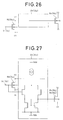
- Fig. 26 is an illustration showing one embodiment of a signal transmission circuit to be employed in the first and second embodiment of the invention;
- Fig. 27 is an illustration showing another embodiment of a signal transmission circuit to be employed in the first and second embodiment of the invention;
- Fig. 28 is an illustration showing one embodiment of a signal transmission circuit to be employed in the third and fourth embodiment of the invention;
- Fig. 29 is an illustration showing another embodiment of a signal transmission circuit to be employed in the third and fourth embodiment of the invention;
- Fig. 30 is an illustration showing first embodiment of a constant current source to be employed in the first to fourth embodiments of the invention;
- Fig. 31 is an illustration showing second embodiment of a constant current source to be employed in the first to fourth embodiments of the invention;
- Fig. 32 is an illustration showing third embodiment of a constant current source to be employed in the first to fourth embodiments of the invention;
- Fig. 33 is an illustration showing fourth embodiment of a constant current source to be employed in the first to fourth embodiments of the invention;
- Fig. 34 is an illustration showing a circuit construction of the fifth embodiment of a sink type differential voltage-to-current converter circuit according to the present invention;
- Fig. 35 is an illustration showing a circuit construction of the fifth embodiment of a source type differential voltage-to-current converter circuit according to the present invention;
- Fig. 36 is an illustration showing an input/output characteristics of the fifth embodiment of the differential voltage-to-current converter circuit according to the invention;
- Fig. 37 is an illustration showing a non-linear characteristics of the fifth embodiment of the differential voltage-to-current converter circuit of the invention;
- Fig. 38 is an illustration showing a circuit construction of the sixth embodiment of a sink type differential voltage-to-current converter circuit according to the present invention;
- Fig. 39 is an illustration showing a circuit construction of the sixth embodiment of a source type differential voltage-to-current converter circuit according to the present invention;
- Fig. 40 is an illustration showing an input/output characteristics of the sixth embodiment of the differential voltage-to-current converter circuit according to the invention; and
- Fig. 41 is an illustration showing a non-linear characteristics of the sixth embodiment of the differential voltage-to-current converter circuit of the invention.
- The preferred embodiments of a MOS differential voltage-to-current converter circuit according to the present invention will be discussed hereinafter with reference to the accompanying drawings.
- Figs. 1 to 4 show a circuit construction of the first embodiment of the MOS differential voltage-to-current converter circuit of the present invention, and an input/output characteristics thereof.
- As shown in Figs. 1 and 2, respective source terminals of first and second MOSFETs (N₁ and N₂ or P₁ and P₂) forming a differential pair in this embodiment are connected to first and second constant current sources I₀₁ and I₀₂. Between the source terminals of the first and second MOSFETs, one source resistor 2R₀ is connected.
- Fig. 1 shows the circuit construction of a sink type MOS differential voltage-to-current converter circuit and Fig. 2 shows the circuit construction of a source type MOS differential voltage-to-current converter circuit.
- In Figs. 1 and 2, the circuit elements performing substantially the same functions to those in the first prior art illustrated in Fig. 13 will be represented by the same reference numerals. N₃ and N₄ of Figs. 1 and 2 denote third and fourth NMOSFETs, and A₁ and A₂ denote first and second signal transmission circuits.
- As the signal transmission circuits A₁ and A₂ in Fig. 1, circuit constructions illustrated in Figs. 26 and 27 can be employed On the other hand, as the signal transmission circuits A₁ and A₂ in Fig. 2, the circuit illustrated in Fig. 27 may be employed. As the constant current source of Fig. 1, various current-mirror circuits illustrated in Figs. 30 to 33 may be employed.
- Hereinafter, the construction and operation of the MOS differential voltage-to-current converter circuit constructed by employing direct connection of Fig. 26 in the first and second signal transmission circuits A₁ and A₂ in Fig. 1.
- As shown in Fig. 1, the third and fourth constant current sources I₀₃ and I₀₄ are connected to the drain terminals of MOSFET N₃ and N₄, respectively for maintaining the gate-source terminal voltages VGS3 and VGS4 of N₃ and N₄ constant. The source terminals of N₃ and N₄ are respectively connected to the source terminals of N₁ and N₂ to maintain the voltage between the first input terminal V₁ and the source terminal of N₁ and the voltage between the second input terminal V₂ and the source terminal of N₂ constant. The drain terminals of N₃ and N₄ are respectively connected to the gate terminals of N₁ and N₂.
- It should be noted that the following condition is established with respect to the constant current sources I₀₁, I₀₂, I₀₃ and I₀₄.


Under the condition set forth above, the operation of the differential voltage-to-current converter circuit of Fig. 1 will be discussed hereinafter . A current which is double of the current of first or second constant current source I₀₁ or I₀₂ is assumed as I₀₀ (equation (25-a)). Also, a current double of the current of the third or fourth constant current source I₀₃ or I₀₄ is assumed as I₀₀' (equation (25-b)). The differential input voltage ΔV can be derived from a difference of the first and second input terminal voltages V₁ and V₂ (equation (26)). - The voltage at opposite ends of the source resistor 2R₀ is expressed by ΔVR. Then, in the loop of V₁ ∼VGS3∼ΔVR∼VGS4∼V₂, the equation (28-a) can be established from Kirchhoff's law. The gate-source terminal voltages VGS3 and VGS4 of NMOSFET N₃ and N₄ can be expressed by the equation (27) in the saturation region. Here, VT3 and VT4 are threshold voltages of N₃ and N₄.
- To the drain terminals of N₃ and N₄, constant currents flow from respective constant current sources I₀₃ and I₀₄. Therefore, as can be appreciated from the equation (27), the gate-source terminal voltages VGS3 and VGS4 become constant. Substituting the equation (27) with VGS3 and VGS4 of the equation (28-a), the equation (28-b) can be established.
- Values in the parenthesis of the equation (28-b), namely (VGS3 - VGS4), becomes a constant value independent of the differential input voltage ΔV. Expressing the term in the parenthesis as -b, ΔVR can be expressed with a linear equation of the differential input voltage ΔV. In this case, the constant b is an offset voltage.
- In the case where circuit elements arranged at symmetrical positions have the same characteristics, the currents of the third and fourth constant current sources I₀₃ and I₀₄, the gains β₃ and β₄, the threshold voltages VT3 and VT4 become mutually equal to each other, respectively. Therefore, VGS3 and VGS4 match to each other. Therefore, the constant b in the equation (28-c) becomes 0. Then, the voltage ΔVR becomes equal to the differential input voltage ΔV (equation (32-a)).
- Next, assuming the current flowing through the resistor 2R₀ is IR0, the equation (29-a) can be established from the Kirchhoff's law with respect to the opposite ends of the resistor 2R₀. Form this. the differential output current ΔI can be expressed by the equation (30-a).
- With respect to the voltage ΔVR at opposite ends of the resistor 2R₀, IR0 can be derived from the equation (29-b). When, the equation (28-b) is employed as ΔVR, the equation (29-c) can be established. Substituting the equation (30-a) with the equation (29-c), the differential output current ΔI can be expressed by the equation (30-b). As can be appreciated from the equation (30-b), the differential output current ΔI is in a linear relationship with the differential input voltage ΔV. This relationship can be expressed by the equation (30-c). Here, constants c and d are respectively derived from the equation (30-d) and the constant b represents (-VGS3 + VGS4) similarly to (28-d). It should be noted that the constant c represents the mutual conductance and the constant d is an offset current.
- With respect to I₀₃ and I₀₄ satisfying Kirchhoff's law at opposite ends of the resistor 2R₀, the drain voltages of NMOSFETs N₃ and N₄ are determined and applied to the gate terminals of the differential pair N₁ and N₂.





- In the case where the circuit elements located at the symmetric positions on the circuit diagram have the same characteristics, the equations (25-a) and (25-b) are established, and gain coefficients β₃ and β₄ of N₃ and N₄ and the threshold voltages VT3 and VT4 of N₃ and N₄ become equal to each other. Then, the constant d in the equation (30-c) becomes 0. Therefore, as shown in the equation (32-b), ΔI becomes proportional to ΔV.
- Similarly manner to the prior arts, the mutual conductance gm and non-linearity E of the shown embodiment of the differential voltage-to-current converter are derived (equations (33-b) and (34-b)). Then, the range of ΔV and ΔI, in which the satisfactory linearity is established is expressed by the equation (35).
- Fig. 3 shows the input/output characteristics of the shown embodiment of the differential voltage-to-current converter circuit and Fig. 4 shows the characteristics of the non-linearity E in relation to the differential input voltage ΔV.





Referring to Figs. 3 and 4, in the differential voltage-to-current converter circuit in the shown embodiment, even when the differential output current ΔI is increased according to increasing of the differential input voltage ΔV, the non-linearity E is not increased and to be maintained at 0 within the range defined by the foregoing equation (35). - Next, discussion will be given for the construction and operation of the differential voltage-to-current converter circuit in the case where the circuit shown in Fig. 27 is employed as the first and second signal transmission circuits A₁ and A₂.
- Each of the source terminals of N₃ and N₄ which are connected to the constant current sources I₀₃ and I₀₄ at the drain terminals for maintaining the gate-source terminal voltages VGS3 and VGS4 constant, is connected to the source terminal of each of N₁ and N₂ as the differential pair so that the voltage between the first input terminal V₁ and the source terminal of N₁ and the voltage between the second input terminal V₂ and the source terminal of N₂ are constant.
- As shown in Fig. 27, the signal transmission circuit A₁ and A₂ respectively comprise differential amplifier circuits . To non-inverting inputs of the differential amplifiers A₁ and A₂, the first and second input terminals V₁ and V₂ are connected. On the other hand, to the inverting inputs, the drain terminals of N₃ and N₄ are connected. Outputs of the differential amplifier circuits A₁ and A₂ are connected to the gate terminals of the first and second NMOSFETs N₁ and N₂, respectively. The input/output characteristics, mutual conductance and non-linearity of the differential voltage-to-current converter circuit employing the differential amplifiers A₁ and A₂ as the first and second signal transmission circuits, can be derived in the similar manner to the case of the foregoing embodiment with direct connection.
- Discussion will be given hereinafter with respect to the operation of the differential voltage-to-current converter circuit employing the differential amplifier circuits A₁ and A₂. When the voltage V₁ at the first input terminal is risen (the voltage V₂ of the second input terminal drops) , the drain voltage of N₃ is lowered (the drain voltage of N₄ is risen). Then, the output of the differential amplifier circuit A₁ is risen and the output of the differential amplifier circuit A₂ is lowered. These outputs are applied to respective gate terminals of N₁ and N₂ of the differential pair. Therefore, the drain current of N₁ is increased and the drain current of N₂ is decreased. Then, the difference of the drain currents of N₁ and N₂ flows through the source resistor 2R₀.
- Accordingly, the differential amplifier circuits A₁ and A₂ operate to maintain the gate-source terminal voltages VGS3 and VGS4 of N₃ and N₄. Namely, they compensate following up of the source terminals of N₃ and N₄ to the first and second input terminals and whereby stabilize the operation of the differential voltage-to-current converter circuit. If the amplification factors of the differential amplifier circuits A₁ and A₂ are sufficiently high, VGS3 and VGS4 can be maintained constant. Then, the mutual conductance gm and the non-linearity E can be expressed by the equations (33-b) and (34-b).
- Next, discussion will be given for the operation in the case where the differential amplifier circuits of Fig. 27 are employed as the signal transmission circuits A₁ and A₂ of the differential voltage-to-current converter circuit shown in Fig. 2. As shown in Fig. 27, non-inverting inputs of the differential amplifier circuits A₁ and A₂ are connected to first and second input terminals V₁ and V₂, respectively. On the other hand, the inverting inputs are connected to the drain terminals of N₃ and N₄. The outputs of the differential amplifier circuits A₁ and A₂ are connected to gate terminals of first and second PMOSFETs P₁ and P₂.
- When the voltage V₁ at the first input terminal is risen (the voltage V₂ of the second input terminal drops) , the drain voltage of N₃ is lowered (the drain voltage of N₄ is risen) . Then, the output of the differential amplifier circuit A₁ is risen and the output of the differential amplifier circuit A₂ is lowered. These outputs are applied to respective gate terminals of P₁ and P₂ of the differential pair. Therefore, the drain current of P₁ is decreased and the drain current of P₂ is increased. Then, the difference of the drain currents of P₁ and P₂ flows through the source resistor 2R₀. The differential amplifier circuits A₁ and A₂ operate to maintain the gate-source terminal voltages VGS3 and VGS4 of N₃ and N₄. Namely, they compensate following up of the source terminals of N₃ and N₄ to the first and second input terminals and whereby stabilize the operation of the differential voltage-to-current converter circuit. If the amplification factors of the differential amplifier circuits A₁ and A₂ are sufficiently high, VGS3 and VGS4 can be maintained constant. Then, the mutual conductance gm and the non-linearity can be expressed by the equations (33-b) and (34-b).
- In this embodiment, the input/output characteristics and the non-linearity of the differential voltage-to-current converter circuit may be derived in the similar manner even when the inputs of the first and second signal transmission circuits A₁ and A₂ are first and second input terminals.
- On the other hand, in the shown embodiment, it is possible to similarly handle the circuit even when the NMOSFET is replaced with the PMOSFET, PMOSFET is replaced with NMOSFET, and the direction of the constant current source is reversed.
- Figs. 5 ∼ 8 show the circuit construction, input/output characteristics of the second embodiment of the MOS differential voltage-to-current converter circuit according to the present invention.
- As shown in Figs. 5 and 6, respective source terminals of first and second MOSFETs (N₁ and N₂ or P₁ and P₂) forming a differential pair in this embodiment are connected to one terminals of first and second resistors R₀₁ and R₀₂. The other terminals of the first and second source resistors R₀₁ and R₀₂ are commonly connected. To the junction of common connection of the first and second resistors R₀₁ and R₀₂ is connected to a constant current source I₀.
- Fig. 5 shows the circuit construction of a sink type MOS differential voltage-to-current converter circuit and Fig. 6 shows the circuit construction of a source type MOS differential voltage-to-current converter circuit. In Fig. 5, the functionally common elements to those in Fig. 16 which illustrates the second prior art will be represented by the same reference numerals. In Fig. 5, N₃ and N₄ are third and fourth NMOSFETs, and VB3 and VB4 are backgate terminals and voltages.
- As the signal transmission circuits A₁ and A₂ in the shown embodiment, circuit constructions illustrated in Figs. 26 and 27 can be employed On the other hand, as the signal transmission circuits A₁ and A₂ in Fig. 6, the circuit illustrated in Fig. 27 may be employed. As the constant current sources of Figs. 5 and 6, various current-mirror circuits illustrated in Figs. 30 to 33 may be employed.
- Hereinafter, the construction and operation of the MOS differential voltage-to-current converter circuit constructed by employing direct connection of Fig. 26 in the first and second signal transmission circuits A₁ and A₂ in Fig. 5.
- As shown in Fig. 5, the constant current sources I₀₃ and I₀₄ are connected to the drain terminals of MOSFET N₃ and N₄, respectively for maintaining the gate-source terminal voltages VGS3 and VGS4 of N₃ and N₄ constant. The source terminals of N₃ and N₄ are respectively connected to the source terminals of N₁ and N₂ to maintain the voltage between the first input terminal V₁ and the source terminal of N₁ and the voltage between the second input terminal V₂ and the source terminal of N₂ constant. The drain terminals of N₃ and N₄ are respectively connected to the gate terminals of N₁ and N₂.
- It should be noted that the following condition is established with respect to the constant current sources I₀, I₀₃ and I₀₄.

Under the condition set forth above, the operation of the differential voltage-to-current converter circuit of Fig. 5 will be discussed hereinafter . The voltage at opposite ends of the first and second resistors R₀₁ and R₀₂ are expressed by ΔVR. Then, in the loop of V₁ ∼VGS3∼ΔVR∼VGS4∼V₂, the equation (38-a) can be established from Kirchhoff's law. Substituting the equation (27) with VGS3 and VGS4 of the equation (38-a), the equation (38-b) can be established. Term in the parenthesis of the equation (38-b), becomes independent of the differential input voltage ΔV. Expressing the term in the parenthesis as -b, ΔVR can be expressed with a linear equation (equation (38-c)). - Assuming the current of the first and second resistors R₀₁ and R₀₂ of Fig. 5 are IR01 and IR02 , and the equation (39) is established on the basis of Kirchhoff's law with respect to the common junction, the voltage ΔVR at opposite ends of the resistors R₀₁ and R₀₂ is expressed by the equation (40), From the equations (39) and (40), the currents IR01 and IR02 can be expressed by the equation (41). From the equation (39) based on Kirchhoff's law, the differential output current ΔI is expressed by the equation (42-a). By substituting the equation (42-a) with IR01 and IR02 of the equation (41), the equation (42-b) can be established. By substituting ΔVR of the equation (42-b) with the equation (38-b), the equation (42-c) is established. Thus, a linear relational expression of the differential output current ΔI and the differential input voltage ΔV can be derived (equation (42-d). It should be noted that constants c and d are defined by equations (42-e) and (42-f).
- In the case where circuit elements arranged at symmetrical positions have the same characteristics, the equations (36-a), (36-b) and (43) are established. Then, the constant b becomes 0. Therefore, ΔVR becomes equal to ΔV, and ΔI becomes proportional to ΔV (equations (45-a) and (45-b)). Fig. 7 shows the input/output characteristics of the shown embodiment.






The mutual conductance gm, non-linearity E and the range to be established are defined by the equations (46) to (48). The characteristic curve of the non-linearity E is illustrated in Fig. 8.





From the equation (47-b) and Figs. 7 and 8, it should be appreciated that even when the differential output current ΔI is increased according to increasing of the differential input voltage ΔV, the non-linearity E is not increased, and maintained 0 within the range defined by the equation (48). - In the shown embodiment, it is possible to similarly handle the circuit even when the NMOSFET is replaced with the PMOSFET, PMOSFET is replaced with NMOSFET, and the direction of the constant current source is reversed.
- Next, discussion will be given for the operation in the case where the differential amplifier circuits of Fig. 27 are employed as the signal transmission circuits A₁ and A₂ of the shown embodiment of the differential voltage-to-current converter circuit. The non-inverting inputs of the differential amplifier circuits A₁ and A₂ are connected to first and second input terminals V₁ and V₂, respectively. On the other hand, the inverting inputs are connected to the drain terminals of N₃ and N₄. The outputs of the differential amplifier circuits A₁ and A₂ are connected to gate terminals of first and second NMOSFETs N₁ and N₂.
- The input/output characteristics and the non-linearity E can be derived in the similar manner to the foregoing first embodiment. Also, the operation is as set forth above, the differential amplifier circuits A₁ and A₂ operate to maintain the gate-source terminal voltages VGS3 and VGS4 of N₃ and N₄. Namely, they compensate following up of the source terminals of N₃ and N₄ to the first and second input terminals and whereby stabilize the operation of the differential voltage-to-current converter circuit. The mutual conductance gm and the non-linearity E are defined by the equations (46-b) and (47-b).
- In the case where the differential amplifier circuits of Fig. 27 are employed as the signal transmission circuits A₁ and A₂ of the differential voltage-to-current converter circuit of Fig. 6, the non-inverting inputs of the differential amplifier circuits A₁ and A₂ are connected to first and second input terminals V₁ and V₂, respectively. On the other hand, the inverting inputs are connected to the drain terminals of N₃ and N₄. The outputs of the differential amplifier circuits A₁ and A₂ are connected to gate terminals of first and second PMOSFETs P₁ and P₂. The input/output characteristics and the non-linearity E of the differential voltage-to-current converter circuit constructed as set forth above can be derived in the similar manner to the foregoing first embodiment. The differential amplifier circuits A₁ and A₂ operate to maintain the gate-source terminal voltages VGS3 and VGS4 of N₃ and N₄. Namely, they compensate following up of the source terminals of N₃ and N₄ to the first and second input terminals and whereby stabilize the operation of the differential voltage-to-current converter circuit. The mutual conductance gm and the non-linearity E are defined by the equations (46-b) and (47-b).
- Figs. 9 and 10 shows the third embodiment of the differential voltage-to-current converter circuit of the present invention. Fig. 9 shows the differential voltage-to-current circuit which is constructed by replacing NMOSFETs N₁ and N₂ in the differential voltage-to-current converter circuit of Fig. 1 with PMOSFETs P₁ and P₂. Also, Fig. 10 shows the embodiment, in which the PMOSFETs P₁ and P₂ of Fig. 2 with NMOSFETs N₁ and N₂. The resistor 2R₀ is connected between the drain terminals of P₁ and P₂ or N₁ and N₂ of the differential pair, In Figs. 9 and 10, like circuit elements to those of Figs. 1 and 2 will be represented by the same reference numerals.
- Fig. 9 shows the circuit construction of a sink type MOS differential voltage-to-current converter circuit and Fig. 10 shows the circuit construction of a source type MOS differential voltage-to-current converter circuit.
- As the signal transmission circuits A₁ and A₂ in the shown embodiment, circuit constructions illustrated in Figs. 28 and 29 can be employed On the other hand, as the signal transmission circuits A₁ and A₂ in Fig. 10, the circuit illustrated in Fig. 28 may be employed. As the constant current source, various current-mirror circuits illustrated in Figs. 30 to 33 may be employed.
- The input/output characteristics and the non-linearity E of the shown embodiment can be derived in the similar manner to the first embodiment. Thus, equivalent characteristics to the first embodiment can be obtained.
- Figs. 11 and 12 shows the third embodiment of the differential voltage-to-current converter circuit of the present invention. Fig. 9 shows the differential voltage-to-current circuit which is constructed by replacing NMOSFETs N₁ and N₂ in the differential voltage-to-current converter circuit of Fig. 1 with PMOSFETs P₁ and P₂. Also, Fig. 10 shows the embodiment, in which the PMOSFETs P₁ and P₂ of Fig. 2 with NMOSFETs N₁ and N₂. The first and second resistors R₀₁ and R₀₂ are connected between the drain terminals of P₁ and P₂ or N₁ and N₂ of the differential pair, In Figs. 11 and 12, like circuit elements to those of Figs. 5 and 6 will be represented by the same reference numerals.
- Fig. 11 shows the circuit construction of a sink type MOS differential voltage-to-current converter circuit and Fig. 12 shows the circuit construction of a source type MOS differential voltage-to-current converter circuit.
- As the signal transmission circuits A₁ and A₂ in the shown embodiment of Fig. 11, circuit constructions illustrated in Figs. 28 and 29 can be employed On the other hand, as the signal transmission circuits A₁ and A₂ in Fig. 12, the circuit illustrated in Fig. 29 may be employed. As the constant current source, various current-mirror circuits illustrated in Figs. 30 to 33 may be employed.
- The input/output characteristics and the non-linearity E of the shown embodiment can be derived in the similar manner to the second embodiment. Thus, equivalent characteristics to the first embodiment can be obtained.
- Concerning the first to fourth embodiments of the present invention, it is regarded that the constant current I₀ connected to the common junction of the first and second resistors and the first and second constant currents I₀₁ and I₀₂ connected to the source terminals of the first and second MOSFETs are ideal constant currents. Also, it is assumed that respective currents satisfies the following equation, then these embodiments of the differential voltage-to-current converters may show equivalent characteristics.

On the other hand, the first and second signal transmission circuits A₁ and A₂ in the foregoing first to fourth embodiments of the invention may be constructed by source followers, voltage followers having amplification factor being 1 or so forth, in addition to the differential amplifiers and direct connection. - As set forth in the first and second embodiments, in the differential voltage-to-current converter circuit according to the shown embodiments, the linearity of the input/output characteristics can be maintained even when the constant current sources I₀₁ to I₀₄, MOSFETs N₁ to N₄ or P₁ to P₄ and so forth placed at symmetric positions on the circuit diagram do no have the same characteristics. Namely, even when the characteristics of each pair of circuit elements are not the same, the relationship between the differential input voltage ΔV and the voltage ΔVR at opposite ends of source (drain) resistor can be expressed by the general equation


- Concerning the mutual conductance and the non-linearity E of the shown embodiments of the differential voltage-to-current converter circuits, the relationship expressed by the equations (33-b) and (34-b) or (46-b) and (47-b) within a range defined by the equation (49) or (50).


Figs. 34, 35, 36 and 37 show the circuit construction, and input/output characteristics of the fifth embodiment of the differential voltage-to-current converter circuit according to the present invention. - The shown embodiment (Figs. 34 and 35) of the differential voltage-to-current converter circuit is constructed by connecting the first and second constant current sources I₀₁ and I₀₂ to the first and second MOSFETs (N₁ and N₂ or P₁ and P₂). One resistor 2R₀ is connected between the source terminals of the first and second MOSFETs.
- Fig. 34 shows the circuit construction of a sink type MOS differential voltage-to-current converter circuit and Fig. 35 shows the circuit construction of a source type MOS differential voltage-to-current converter circuit.
- The source terminals of the third and fourth MOSFETs are connected to the source terminals of the first and second MOSFETs. The drain terminals of the third and fourth MOSFETs are connected to respective input sides of the first and second current mirror circuits M₁ and M₂. The output terminals of the first and second current-mirror circuits M₁ and M₂ are connected to the third and fourth constant current sources and gate terminals of the first and second MOSFETs. Accordingly, when the input V₁ is risen for example, the gate-source terminal voltage VGS3 is temporarily increased. Associating therewith, the drain current of N₃ and the input current of M₁ are also risen. Here, since I₀₃ is constant, the gate voltage of N₁ is swiftly risen. Therefore, I₁ is increased. Subsequently, the voltages at the source terminals of N₁ and N₂ are risen. This increasing of VGS3 can be suppressed. As can be appreciated, such operation is a kind of feedback operation to make the operation of the differential voltage-to-current converter circuit stable. In short, as far as M₁ is in operation in the saturating region, the gate voltage of N₁ converges to the voltage to maintain the current flowing through N₂ constant. Therefore, the voltage VGS3 between V₁ and the source terminal of N₁ and the voltage VGS4 between V₂ and the source terminal of N₂ become constant.
- As set forth above, in the same reason, the output current and linearity equivalent to the first and second embodiments can be obtained.
- Figs. 38 to 41 show the circuit construction, and input/output characteristics of the sixth embodiment of the differential voltage-to-current converter circuit according to the present invention.
- The shown embodiment of the differential voltage-to-current converter circuit is constructed by connecting one terminals of the first and second resistors R₀₁ and R₀₂ to the source terminals of the first and second MOSFETs (N₁ and N₂ or P₁ and P₂). The other terminals of the first and second resistors R₀₁ and R₀₂ are connected in common. The constant current source I0 is connected to the junction of the common connection between the first and second resistors R₀₁ and R₀₂. Fig. 38 shows the circuit construction of a sink type MOS differential voltage-to-current converter circuit and Fig. 39 shows the circuit construction of a source type MOS differential voltage-to-current converter circuit. Here, respective signs in Figs. 38 and 39 have the same meaning to the corresponding signs in Fig. 16 which illustrates the second prior art. N₃ and N₄ represent third and fourth NMOSFETs. The constant current source can be constructed as shown in Figs. 30, 31, 32 and 33.
- Discussion will be given hereinafter with respect to the operation of the circuit construction of Fig. 38. The source terminals of the third and fourth MOSFETs are connected to the source terminals of the first and second MOSFETs. The drain terminals of the third and fourth MOSFETs are connected to respective input sides of the first and second current mirror circuits M₁ and M₂. The output terminals of the first and second current-mirror circuits M₁ and M₂ are connected to the third and fourth constant current sources and the gate terminals of the first and second MOSFETs. Accordingly, when the input V₁ is risen for example, the gate-source terminal voltage VGS3 is temporarily increased. Associating therewith, the drain current of N₃ and the input current of M₁ are also risen. Here, since I₀₃ is constant, the gate voltage of N₁ is swiftly risen. Therefore, I₁ is increased. Subsequently, the voltages at the source terminals of N₁ and N₃ are risen. This increasing of VGS3 can be suppressed. As can be appreciated, such operation is a kind of feedback operation to make the operation of the differential voltage-to-current converter circuit stable. In short, as far as M₁ is in operation in the saturating region, the gate voltage of N₁ converges to the voltage to maintain the current flowing through N₂ constant. Therefore, the voltage VGS3 between V₁ and the source terminal of N₁ and the voltage VGS4 between V₂ and the source terminal of N₂ become constant.
- As set forth above, in the same reason, the output current and linearity equivalent to the first and second embodiments can be obtained.
- As set forth above, the MOS differential voltage-to-current converter circuit according to the present invention establishes the negative feedback with the shown construction, in which the source (drain) resistors are provided, the source (drain terminals of the first and second MOSFETs are connected to the source terminals of the third and fourth MOSFETs, the drain terminals of the third and fourth MOSFETs are respectively connected to the input sides of the first and second current mirror circuits M₁ and M₂, and the outputs of the current-mirror circuits M₁ and M₂ are connected to the constant current source and the gate terminals of the first and second MOSFETs.
- As a result, as long as the operation is taken placed in the region where M₁ and M₂ are saturated, the gate voltage of N₁ and N₂ are converged at the voltage where the current I₀₃ flowing through N₃ and the current I₀₄ flowing through N₄ are equal to each other so that V₁, the voltage VGS3 between the source terminal of the N₁ and the voltage VGS4 between V₂ and the voltage V₂ and the source terminal of N₄ become constant. Furthermore, there is provided the first and second signal transmission means which has the inputs connected to the respective of the first and second input terminals and/or to the drain terminals of the third and fourth MOSFETs, and the outputs connected to respective gate terminals of the first and second MOSFETs. By the presence of the signal transmission means, the mutual conductance gm of the differential voltage-to-current converter circuit can be determined only by the resistance value 2R₀, R₀₁ + R₀₂ between the source (drain) terminals. Also, even when the differential output current is increased associating with increasing of the differential input voltage, the non-linearity E can be held 0.
- Therefore, with the differential current-to-voltage converter circuit according to the present invention, it becomes possible to avoid increasing of non-linearity due to influence of various property of the differential MOSFET (such as, non-linearity of ID-VGS characteristics, fluctuation of the gain coefficient β, variation of the threshold voltage VT due to backgate effect, saturation of MOS due to end channel effect and so forth, variation of the ID-VDS characteristics within the non-saturated range and so forth) , within a predetermined range of the differential input voltage.
- Characteristics variation factor of the MOSFET is quite large in comparison with that of the bipolar transistor and is specific to the MOSFET. Conventionally, such characteristics variation was inevitable in the MOSFET circuit. According to the present invention, even when the circuit elements located at symmetric positions on the circuit diagram do not have the same characteristics, the relationship between the differential input voltage ΔV and the voltage ΔVR at opposite ends of the source (drain) resistor and the relationship between the differential input voltage ΔV and the differential output current ΔI can be maintained linear without depending upon the characteristics variation of the MOSFETs. Therefore, the linearity of the differential voltage-to-current converter can be significantly improved.
- Furthermore, the differential voltage-to-current converter circuit can be fabricated through a MOS process, which can simply the fabrication process contributing lowering of the production cost.
- Although the invention has been illustrated and described with respect to exemplary embodiment thereof, it should be understood by those skilled in the art that the foregoing and various other changes, omissions and additions may be made therein and thereto, without departing from the spirit and scope of the present invention. Therefore, the present invention should not be understood as limited to the specific embodiment set out above but to include all possible embodiments which can be embodies within a scope encompassed and equivalents thereof with respect to the feature set out in the appended claims.
Claims (26)
- A MOS differential voltage-to-current converter circuit comprising:
first and second MOS transistors;
a resistor connected between the sources of said first and second MOS transistors;
a first constant current source for supplying operation current for said first and second MOS transistors;
third and fourth MOS transistors having sources respectively connected to the source of said first and second MOS transistors and receiving a differential input voltage at the gates thereof;
second and third constant current sources for supplying operation currents for said third and fourth MOS transistors; and
first and second signal transmission means for transmitting drain outputs of said third and fourth MOS transistors to the gates of said first and second MOS transistors for taking the current flowing through said first and second MOS transistors as a differential output. - A MOS differential voltage-to-current converter circuit as set forth in claim 1, wherein said first and second signal transmission means comprises one of an amplifier circuit, an attenuation circuit and a voltage follower circuit.
- A MOS differential voltage-to-current converter circuit as set forth in claim 1, wherein said first constant current source comprises two constant current sources respectively supplying operation currents to respective of said first and second MOS transistors.
- A MOS differential voltage-to-current converter circuit as set forth in claim 1, wherein all of said first to fourth MOS transistors are the transistors of the same conductive type.
- A MOS differential voltage-to-current converter circuit as set forth in claim 1, wherein said first and second MOS transistors, and said third and fourth MOS transistors have mutually opposite conductive types.
- A MOS differential voltage-to-current converter circuit as set forth in claim 1, wherein said resistor comprises first and second resistor elements which are connected in series, and said first constant current source supplies the operation current at the junction of series connection of said first and second resistor elements.
- A MOS differential voltage-to-current converter circuit comprising:
first and second MOS transistors;
a resistor connected between the sources of said first and second MOS transistors;
a first constant current source for supplying operation current for said first and second MOS transistors;
third and fourth MOS transistors having sources respectively connected to the source of said first and second MOS transistors and receiving a differential input voltage at the gates thereof;
a first differential amplifier circuit receiving a gate input and a drain output of said third MOS transistor as inputs and applying an output as said differential output to the gate of said first MOS transistor; and
a second differential amplifier circuit receiving a gate input and a drain output of said fourth MOS transistor as inputs and applying an output as said differential output to the gate of said second MOS transistor for taking the current flowing through said first and second MOS transistors as a differential output. - A MOS differential voltage-to-current converter circuit as set forth in claim 7, wherein said first constant current source supplies the operation current for said first and second MOS transistors.
- A MOS differential voltage-to-current converter circuit as set forth in claim 7, wherein said first and second MOS transistors, and said third and fourth MOS transistors have mutually opposite conductive types.
- A MOS differential voltage-to-current converter circuit as set forth in claim 7, wherein said resistor comprises first and second resistor elements which are connected in series, and said first constant current source supplies the operation current at the junction of series connection of said first and second resistor elements.
- A MOS differential voltage-to-current converter circuit comprising:
first and second MOS transistors;
a resistor connected between the drains of said first and second MOS transistors;
a first constant current source for supplying operation current for said first and second MOS transistors;
third and fourth MOS transistors having sources respectively connected to the drain of said first and second MOS transistors and receiving a differential input voltage at the gates thereof;
second and third constant current sources for supplying operation currents for said third and fourth MOS transistors; and
first and second signal transmission means for transmitting drain outputs of said third and fourth MOS transistors to the gates of said first and second MOS transistors for taking the current flowing through said first and second MOS transistors as a differential output. - A MOS differential voltage-to-current converter circuit as set forth in claim 11, wherein said first and second signal transmission means comprises one of an amplifier circuit, an attenuation circuit and a voltage follower circuit.
- A MOS differential voltage-to-current converter circuit as set forth in claim 11, wherein said first constant current source comprises two constant current sources respectively supplying operation currents to respective of said first and second MOS transistors.
- A MOS differential voltage-to-current converter circuit as set forth in claim 11, wherein all of said first to fourth MOS transistors are the transistors of the same conductive type.
- A MOS differential voltage-to-current converter circuit as set forth in claim 11, wherein said first and second MOS transistors, and said third and fourth MOS transistors have mutually opposite conductive types.
- A MOS differential voltage-to-current converter circuit as set forth in claim 11, wherein said resistor comprises first and second resistor elements which are connected in series, and said first constant current source supplies the operation current at the junction of series connection of said first and second resistor elements.
- A MOS differential voltage-to-current converter circuit comprising:
first and second MOS transistors;
a resistor connected between the drains of said first and second MOS transistors;
a first constant current source for supplying operation current for said first and second MOS transistors;
third and fourth MOS transistors having sources respectively connected to the drains of said first and second MOS transistors and receiving a differential input voltage at the gates thereof;
a first differential amplifier circuit receiving a gate input and a drain output of said third MOS transistor as inputs and applying an output as said differential output to the gate of said first MOS transistor; and
a second differential amplifier circuit receiving a gate input and a drain output of said fourth MOS transistor as inputs and applying an output as said differential output to the gate of said second MOS transistor for taking the current flowing through said first and second MOS transistors as a differential output. - A MOS differential voltage-to-current converter circuit as set forth in claim 17, wherein said first constant current source supplies the operation current for said first and second MOS transistors.
- A MOS differential voltage-to-current converter circuit as set forth in claim 17, wherein said first and second MOS transistors, and said third and fourth MOS transistors have mutually opposite conductive types.
- A MOS differential voltage-to-current converter circuit as set forth in claim 17, wherein said resistor comprises first and second resistor elements which are connected in series, and said first constant current source supplies the operation current at the junction of series connection of said first and second resistor elements.
- A MOS differential voltage-to-current converter circuit comprising:
first and second MOS transistors;
a resistor connected between the drains of said first and second MOS transistors;
a first constant current source for supplying operation current for said first and second MOS transistors;
third and fourth MOS transistors having sources respectively connected to the drains of said first and second MOS transistors and receiving a differential input voltage at the gates thereof;
a first current-mirror circuit receiving the drain output of said third MOS transistor as a current input and having a current output terminal connected to the gate of said first MOS transistor; and
a second current-mirror circuit receiving the drain output of said fourth MOS transistor as a current input and having a current output terminal connected to the gate of said second MOS transistor for taking the current flowing through said first and second MOS transistors as a differential output. - A MOS differential voltage-to-current converter circuit as set forth in claim 21, which further comprises first and second and third constant current source respectively sinking the output current of said first and second current-mirror circuits.
- A MOS differential voltage-to-current converter circuit as set forth in claim 21, wherein said first constant current source comprises two constant current sources respectively supplying operation currents to respective of said first and second MOS transistors.
- A MOS differential voltage-to-current converter circuit as set forth in claim 21, wherein all of said first to fourth MOS transistors are the transistors of the same conductive type.
- A MOS differential voltage-to-current converter circuit as set forth in claim 21, wherein said first and second MOS transistors, and said third and fourth MOS transistors have mutually opposite conductive types.
- A MOS differential voltage-to-current converter circuit as set forth in claim 21, wherein said resistor comprises first and second resistor elements which are connected in series, and said first constant current source supplies the operation current at the junction of series connection of said first and second resistor elements.
Applications Claiming Priority (6)
| Application Number | Priority Date | Filing Date | Title |
|---|---|---|---|
| JP16561193 | 1993-07-05 | ||
| JP165611/93 | 1993-07-05 | ||
| JP16561193 | 1993-07-05 | ||
| JP318871/93 | 1993-12-20 | ||
| JP31887193 | 1993-12-20 | ||
| JP5318871A JP2944398B2 (en) | 1993-07-05 | 1993-12-20 | MOS differential voltage-current converter |
Publications (3)
| Publication Number | Publication Date |
|---|---|
| EP0633656A2 true EP0633656A2 (en) | 1995-01-11 |
| EP0633656A3 EP0633656A3 (en) | 1995-12-06 |
| EP0633656B1 EP0633656B1 (en) | 2002-06-12 |
Family
ID=26490279
Family Applications (1)
| Application Number | Title | Priority Date | Filing Date |
|---|---|---|---|
| EP94110371A Expired - Lifetime EP0633656B1 (en) | 1993-07-05 | 1994-07-04 | MOS differential voltage-to-current converter circuit |
Country Status (5)
| Country | Link |
|---|---|
| US (3) | US5598117A (en) |
| EP (1) | EP0633656B1 (en) |
| JP (1) | JP2944398B2 (en) |
| KR (1) | KR0126633B1 (en) |
| DE (1) | DE69430778T2 (en) |
Cited By (2)
| Publication number | Priority date | Publication date | Assignee | Title |
|---|---|---|---|---|
| GB2319418A (en) * | 1996-11-15 | 1998-05-20 | Nec Corp | Operational transconductance amplifier with floating resistor |
| DE19951019B4 (en) * | 1999-10-22 | 2007-02-01 | Ott, Reinhold, Waterloo | Device for securing a product against theft |
Families Citing this family (31)
| Publication number | Priority date | Publication date | Assignee | Title |
|---|---|---|---|---|
| JPH08181548A (en) * | 1994-12-26 | 1996-07-12 | Mitsubishi Electric Corp | Differential amplifier circuit, cmos inverter, demodulation circuit for pulse width modulation and sampling circuit |
| JP3171373B2 (en) * | 1995-10-12 | 2001-05-28 | アルプス電気株式会社 | Microcurrent detection circuit and coordinate input device using the same |
| JPH1079656A (en) * | 1996-09-05 | 1998-03-24 | Nec Corp | Current switching type switch circuit |
| US5815390A (en) * | 1996-10-01 | 1998-09-29 | Lucent Technologies Inc. | Voltage-to-current converter |
| JP3881079B2 (en) * | 1997-03-14 | 2007-02-14 | 株式会社アドバンテスト | Semiconductor integrated circuit element |
| JP3105823B2 (en) * | 1997-06-12 | 2000-11-06 | 九州日本電気株式会社 | Voltage-current converter |
| SG68676A1 (en) * | 1997-08-15 | 1999-11-16 | Texas Instruments Inc | Current comparator and method therefor |
| JP4210873B2 (en) * | 1998-01-14 | 2009-01-21 | ソニー株式会社 | Impedance conversion circuit, video equipment, audio equipment and communication device |
| GB2345600B (en) * | 1999-01-09 | 2003-07-30 | Mitel Semiconductor Ltd | Voltage to current converter |
| JP2000223967A (en) * | 1999-01-27 | 2000-08-11 | Toshiba Corp | Signal amplification circuit |
| US6369618B1 (en) * | 1999-02-12 | 2002-04-09 | Texas Instruments Incorporated | Temperature and process independent exponential voltage-to-current converter circuit |
| US6356152B1 (en) * | 1999-07-14 | 2002-03-12 | Texas Instruments Incorporated | Amplifier with folded super-followers |
| DE50012856D1 (en) * | 2000-02-15 | 2006-07-06 | Infineon Technologies Ag | Voltage-current converter |
| US6292034B1 (en) * | 2000-02-24 | 2001-09-18 | Motorola Inc. | Low noise transconductance device |
| US6366167B1 (en) * | 2000-02-29 | 2002-04-02 | Gain Technology Corporation | Low voltage rail-to-rail CMOS input stage |
| US6580326B2 (en) * | 2001-05-25 | 2003-06-17 | Infineon Technologies North America Corp. | High-bandwidth low-voltage gain cell and voltage follower having an enhanced transconductance |
| KR100423494B1 (en) * | 2002-03-07 | 2004-03-18 | 삼성전자주식회사 | Transconductor |
| TWI260857B (en) * | 2002-05-15 | 2006-08-21 | Ind Tech Res Inst | High linearily CMOS transconductor circuit |
| KR100576716B1 (en) * | 2003-12-23 | 2006-05-03 | 한국전자통신연구원 | Transconductor Circuit Compensates for Distortion of Output Current |
| KR100582545B1 (en) * | 2003-12-23 | 2006-05-22 | 한국전자통신연구원 | Transconductor Circuit Compensates for Distortion of Output Current |
| US7239184B2 (en) * | 2005-04-27 | 2007-07-03 | National Instruments Corporation | Low power and high efficiency voltage-to-current converter with improved power supply rejection |
| US7480126B2 (en) * | 2005-04-27 | 2009-01-20 | National Instruments Corporation | Protection and voltage monitoring circuit |
| US7388387B2 (en) * | 2006-01-11 | 2008-06-17 | Stratosphere Solutions, Inc. | Method and apparatus for measurement of electrical resistance |
| US7602220B1 (en) * | 2008-06-24 | 2009-10-13 | Gigle Semiconductor, Ltd. | Resistor-input transconductor including common-mode compensation |
| JP2011228935A (en) * | 2010-04-20 | 2011-11-10 | Olympus Corp | Amplifier circuit |
| JP5523251B2 (en) * | 2010-08-30 | 2014-06-18 | オリンパス株式会社 | Amplifier circuit |
| CN103503342B (en) | 2011-03-04 | 2016-05-04 | Lg电子株式会社 | Method and device for setting backhaul link subframe in wireless communication system with carrier aggregation technology applied |
| US9197458B1 (en) * | 2014-05-01 | 2015-11-24 | Samsung Display Co., Ltd. | Edge equalization via adjustment of unroll threshold for crossing slicer |
| US10998864B1 (en) * | 2019-09-26 | 2021-05-04 | Xilinx, Inc | Non-linearity correction |
| JP2021190845A (en) * | 2020-05-29 | 2021-12-13 | 凸版印刷株式会社 | Gain control amplifier |
| US20240339977A1 (en) * | 2023-04-06 | 2024-10-10 | Texas Instruments Incorporated | Amplifier with input and output common-mode control in a single amplification stage |
Family Cites Families (27)
| Publication number | Priority date | Publication date | Assignee | Title |
|---|---|---|---|---|
| GB1528201A (en) * | 1975-02-24 | 1978-10-11 | Rca Corp | Differential amplifier |
| JPS5532044B2 (en) * | 1972-09-18 | 1980-08-22 | ||
| JPS5412184B2 (en) * | 1973-08-03 | 1979-05-21 | ||
| NL7407953A (en) * | 1974-06-14 | 1975-12-16 | Philips Nv | VOLTAGE CURRENT CONVERTER. |
| GB2213019B (en) * | 1980-08-19 | 1989-10-25 | Elliott Brothers London Ltd | Head-up display systems |
| JPS5746161A (en) * | 1980-09-03 | 1982-03-16 | Mitsubishi Electric Corp | Conversion circuit for voltage/current |
| US4390848A (en) * | 1981-02-12 | 1983-06-28 | Signetics | Linear transconductance amplifier |
| IT1212720B (en) * | 1983-03-23 | 1989-11-30 | Ates Componenti Elettron | HIGH PRECISION VOLTAGE-CURRENT CONVERTER, ESPECIALLY FOR LOW POWER SUPPLY VOLTAGES. |
| JPS59229909A (en) * | 1983-06-11 | 1984-12-24 | Sony Corp | Differential amplifier |
| NL8600422A (en) * | 1986-02-20 | 1987-09-16 | Philips Nv | TRANSCONDUCTION AMPLIFIER. |
| JPH0739341B2 (en) * | 1986-08-09 | 1995-05-01 | 大正製薬株式会社 | Bromhexine hydrochloride anti-adsorption formulation |
| IT1201852B (en) * | 1986-10-21 | 1989-02-02 | Sgs Microelettronica Spa | DIFFERENTIAL AMPLIFIER USING MOS TRANSISTORS WITH CHANNEL OF THE SAME TYPE |
| US4868692A (en) * | 1987-03-31 | 1989-09-19 | Matsushita Electric Industrial Co., Ltd. | Tracking error signal forming circuit |
| US4783602A (en) * | 1987-06-26 | 1988-11-08 | American Telephone And Telegraph Company, At&T Bell Laboratories | Operational transconductance amplifier for use in sample-and-hold circuits and the like |
| US4774476A (en) * | 1987-07-06 | 1988-09-27 | Motorola, Inc. | Linearized differential amplifier |
| US4961046A (en) * | 1988-08-19 | 1990-10-02 | U.S. Philips Corp. | Voltage-to-current converter |
| US4897611A (en) * | 1988-10-28 | 1990-01-30 | Micro Linear Corporation | Very high gain positive feedback CMOS transconductance amplifier |
| JPH03163907A (en) * | 1989-11-22 | 1991-07-15 | Casio Comput Co Ltd | Differential amplifier circuit |
| FR2663476B1 (en) * | 1990-06-19 | 1995-08-04 | Sgs Thomson Microelectronics | LINEAR DIFFERENTIAL AMPLIFIER WITH TRANSCONDUCTANCE. |
| US5113147A (en) * | 1990-09-26 | 1992-05-12 | Minnesota Mining And Manufacturing Company | Wide-band differential amplifier using gm-cancellation |
| US5101126A (en) * | 1990-10-15 | 1992-03-31 | Analog Devices, Inc. | Wide dynamic range transconductance stage |
| US5184087A (en) * | 1991-03-30 | 1993-02-02 | Goldstar Electron Co., Ltd. | Transconductance amplifier using parasitic bipolar transistors to embody a constant voltage source |
| EP0507388A3 (en) * | 1991-04-02 | 1993-01-13 | N.V. Philips' Gloeilampenfabrieken | Differential amplifier with signal-dependent quiescent current control |
| JPH06140847A (en) * | 1992-10-27 | 1994-05-20 | Olympus Optical Co Ltd | Differential amplifier circuit |
| KR100284628B1 (en) * | 1992-11-17 | 2001-03-15 | 요트.게.아. 롤페즈 | MOS technology amplifier circuit |
| US5373248A (en) * | 1993-06-08 | 1994-12-13 | At&T Bell Laboratories | Transconductor employing differential pair composite field effect transistors |
| US5436594A (en) * | 1994-10-18 | 1995-07-25 | Motorola, Inc. | Fully differential transconductance amplifier with common-mode output voltage stabilization |
-
1993
- 1993-12-20 JP JP5318871A patent/JP2944398B2/en not_active Expired - Fee Related
-
1994
- 1994-07-01 US US08/269,789 patent/US5598117A/en not_active Expired - Lifetime
- 1994-07-04 DE DE69430778T patent/DE69430778T2/en not_active Expired - Lifetime
- 1994-07-04 KR KR1019940015893A patent/KR0126633B1/en not_active Expired - Fee Related
- 1994-07-04 EP EP94110371A patent/EP0633656B1/en not_active Expired - Lifetime
-
1995
- 1995-06-02 US US08/458,907 patent/US5552730A/en not_active Expired - Lifetime
- 1995-06-02 US US08/458,776 patent/US5552729A/en not_active Expired - Lifetime
Cited By (2)
| Publication number | Priority date | Publication date | Assignee | Title |
|---|---|---|---|---|
| GB2319418A (en) * | 1996-11-15 | 1998-05-20 | Nec Corp | Operational transconductance amplifier with floating resistor |
| DE19951019B4 (en) * | 1999-10-22 | 2007-02-01 | Ott, Reinhold, Waterloo | Device for securing a product against theft |
Also Published As
| Publication number | Publication date |
|---|---|
| KR950004709A (en) | 1995-02-18 |
| US5598117A (en) | 1997-01-28 |
| JPH0774555A (en) | 1995-03-17 |
| US5552730A (en) | 1996-09-03 |
| DE69430778D1 (en) | 2002-07-18 |
| JP2944398B2 (en) | 1999-09-06 |
| DE69430778T2 (en) | 2003-02-20 |
| KR0126633B1 (en) | 1997-12-30 |
| US5552729A (en) | 1996-09-03 |
| EP0633656A3 (en) | 1995-12-06 |
| EP0633656B1 (en) | 2002-06-12 |
Similar Documents
| Publication | Publication Date | Title |
|---|---|---|
| EP0633656B1 (en) | MOS differential voltage-to-current converter circuit | |
| US5594383A (en) | Analog filter circuit and semiconductor integrated circuit device using the same | |
| US7746168B2 (en) | Bias circuit | |
| US5068621A (en) | Compensation method and apparatus for enhancing single-ended to differential conversion | |
| JPH03114305A (en) | Current mirror circuit | |
| GB2290187A (en) | Mos operational transconductance amplifier | |
| EP0045841A1 (en) | Linear voltage-current converter | |
| GB1591918A (en) | Current mirror amplifier circuit | |
| KR0177511B1 (en) | Linear CMOS Output Stage | |
| US7038501B2 (en) | Transconductor circuit for compensating the distortion of output current | |
| US7248116B2 (en) | Differential amplifiers | |
| EP0283865A1 (en) | Pinchoff voltage generator | |
| EP0813163B1 (en) | Variable level shifter and multiplier suitable for low-voltage, differential operation | |
| US20210250006A1 (en) | Output pole-compensated operational amplifier | |
| KR20220136184A (en) | Reference Current Source | |
| US5097156A (en) | Circuitry for compensating for transistor parameter mismatches in a CMOS analog four-quadrant multiplier | |
| US5656964A (en) | CMOS low-voltage four-quadrant multiplier | |
| Nauta et al. | A CMOS triode transconductor | |
| JPH03274911A (en) | Operational amplifier | |
| US6566959B2 (en) | Amplifier circuit having a particular biasing arrangement | |
| KR100582545B1 (en) | Transconductor Circuit Compensates for Distortion of Output Current | |
| KR100423494B1 (en) | Transconductor | |
| US4333025A (en) | N-Channel MOS comparator | |
| Aiyappa et al. | Amplifier design in weak inversion and strong inversion—A case study | |
| Oliaei et al. | A CMOS class AB current-multiplier |
Legal Events
| Date | Code | Title | Description |
|---|---|---|---|
| PUAI | Public reference made under article 153(3) epc to a published international application that has entered the european phase |
Free format text: ORIGINAL CODE: 0009012 |
|
| AK | Designated contracting states |
Kind code of ref document: A2 Designated state(s): DE FR GB |
|
| PUAL | Search report despatched |
Free format text: ORIGINAL CODE: 0009013 |
|
| AK | Designated contracting states |
Kind code of ref document: A3 Designated state(s): DE FR GB |
|
| 17P | Request for examination filed |
Effective date: 19951024 |
|
| 17Q | First examination report despatched |
Effective date: 19961210 |
|
| GRAG | Despatch of communication of intention to grant |
Free format text: ORIGINAL CODE: EPIDOS AGRA |
|
| GRAG | Despatch of communication of intention to grant |
Free format text: ORIGINAL CODE: EPIDOS AGRA |
|
| GRAG | Despatch of communication of intention to grant |
Free format text: ORIGINAL CODE: EPIDOS AGRA |
|
| GRAG | Despatch of communication of intention to grant |
Free format text: ORIGINAL CODE: EPIDOS AGRA |
|
| GRAH | Despatch of communication of intention to grant a patent |
Free format text: ORIGINAL CODE: EPIDOS IGRA |
|
| GRAH | Despatch of communication of intention to grant a patent |
Free format text: ORIGINAL CODE: EPIDOS IGRA |
|
| GRAA | (expected) grant |
Free format text: ORIGINAL CODE: 0009210 |
|
| AK | Designated contracting states |
Kind code of ref document: B1 Designated state(s): DE FR GB |
|
| REG | Reference to a national code |
Ref country code: GB Ref legal event code: FG4D |
|
| REF | Corresponds to: |
Ref document number: 69430778 Country of ref document: DE Date of ref document: 20020718 |
|
| ET | Fr: translation filed | ||
| REG | Reference to a national code |
Ref country code: GB Ref legal event code: 732E |
|
| PLBE | No opposition filed within time limit |
Free format text: ORIGINAL CODE: 0009261 |
|
| STAA | Information on the status of an ep patent application or granted ep patent |
Free format text: STATUS: NO OPPOSITION FILED WITHIN TIME LIMIT |
|
| 26N | No opposition filed |
Effective date: 20030313 |
|
| REG | Reference to a national code |
Ref country code: FR Ref legal event code: TP |
|
| REG | Reference to a national code |
Ref country code: FR Ref legal event code: CD |
|
| PGFP | Annual fee paid to national office [announced via postgrant information from national office to epo] |
Ref country code: GB Payment date: 20110629 Year of fee payment: 18 |
|
| PGFP | Annual fee paid to national office [announced via postgrant information from national office to epo] |
Ref country code: FR Payment date: 20110727 Year of fee payment: 18 |
|
| PGFP | Annual fee paid to national office [announced via postgrant information from national office to epo] |
Ref country code: DE Payment date: 20110629 Year of fee payment: 18 |
|
| REG | Reference to a national code |
Ref country code: DE Ref legal event code: R082 Ref document number: 69430778 Country of ref document: DE Representative=s name: GLAWE DELFS MOLL - PARTNERSCHAFT VON PATENT- U, DE |
|
| REG | Reference to a national code |
Ref country code: DE Ref legal event code: R082 Ref document number: 69430778 Country of ref document: DE Representative=s name: GLAWE DELFS MOLL - PARTNERSCHAFT VON PATENT- U, DE Effective date: 20120828 Ref country code: DE Ref legal event code: R081 Ref document number: 69430778 Country of ref document: DE Owner name: RENESAS ELECTRONICS CORPORATION, JP Free format text: FORMER OWNER: NEC ELECTRONICS CORP., KAWASAKI, JP Effective date: 20120828 |
|
| GBPC | Gb: european patent ceased through non-payment of renewal fee |
Effective date: 20120704 |
|
| REG | Reference to a national code |
Ref country code: FR Ref legal event code: ST Effective date: 20130329 |
|
| PG25 | Lapsed in a contracting state [announced via postgrant information from national office to epo] |
Ref country code: GB Free format text: LAPSE BECAUSE OF NON-PAYMENT OF DUE FEES Effective date: 20120704 Ref country code: DE Free format text: LAPSE BECAUSE OF NON-PAYMENT OF DUE FEES Effective date: 20130201 Ref country code: FR Free format text: LAPSE BECAUSE OF NON-PAYMENT OF DUE FEES Effective date: 20120731 |
|
| REG | Reference to a national code |
Ref country code: DE Ref legal event code: R119 Ref document number: 69430778 Country of ref document: DE Effective date: 20130201 |