EP0635162B1 - Ecran de visualisation plat autoporteur - Google Patents
Ecran de visualisation plat autoporteur Download PDFInfo
- Publication number
- EP0635162B1 EP0635162B1 EP93911573A EP93911573A EP0635162B1 EP 0635162 B1 EP0635162 B1 EP 0635162B1 EP 93911573 A EP93911573 A EP 93911573A EP 93911573 A EP93911573 A EP 93911573A EP 0635162 B1 EP0635162 B1 EP 0635162B1
- Authority
- EP
- European Patent Office
- Prior art keywords
- addressing
- layers
- holes
- grid
- traces
- Prior art date
- Legal status (The legal status is an assumption and is not a legal conclusion. Google has not performed a legal analysis and makes no representation as to the accuracy of the status listed.)
- Expired - Lifetime
Links
Images










Classifications
-
- H—ELECTRICITY
- H01—ELECTRIC ELEMENTS
- H01J—ELECTRIC DISCHARGE TUBES OR DISCHARGE LAMPS
- H01J61/00—Gas-discharge or vapour-discharge lamps
- H01J61/02—Details
- H01J61/30—Vessels; Containers
-
- H—ELECTRICITY
- H01—ELECTRIC ELEMENTS
- H01J—ELECTRIC DISCHARGE TUBES OR DISCHARGE LAMPS
- H01J17/00—Gas-filled discharge tubes with solid cathode
- H01J17/38—Cold-cathode tubes
- H01J17/48—Cold-cathode tubes with more than one cathode or anode, e.g. sequence-discharge tube, counting tube, dekatron
- H01J17/49—Display panels, e.g. with crossed electrodes, e.g. making use of direct current
-
- H—ELECTRICITY
- H01—ELECTRIC ELEMENTS
- H01J—ELECTRIC DISCHARGE TUBES OR DISCHARGE LAMPS
- H01J29/00—Details of cathode-ray tubes or of electron-beam tubes of the types covered by group H01J31/00
- H01J29/02—Electrodes; Screens; Mounting, supporting, spacing or insulating thereof
- H01J29/028—Mounting or supporting arrangements for flat panel cathode ray tubes, e.g. spacers particularly relating to electrodes
-
- H—ELECTRICITY
- H01—ELECTRIC ELEMENTS
- H01J—ELECTRIC DISCHARGE TUBES OR DISCHARGE LAMPS
- H01J29/00—Details of cathode-ray tubes or of electron-beam tubes of the types covered by group H01J31/00
- H01J29/02—Electrodes; Screens; Mounting, supporting, spacing or insulating thereof
- H01J29/08—Electrodes intimately associated with a screen on or from which an image or pattern is formed, picked-up, converted or stored, e.g. backing-plates for storage tubes or collecting secondary electrons
- H01J29/085—Anode plates, e.g. for screens of flat panel displays
-
- H—ELECTRICITY
- H01—ELECTRIC ELEMENTS
- H01J—ELECTRIC DISCHARGE TUBES OR DISCHARGE LAMPS
- H01J29/00—Details of cathode-ray tubes or of electron-beam tubes of the types covered by group H01J31/00
- H01J29/46—Arrangements of electrodes and associated parts for generating or controlling the ray or beam, e.g. electron-optical arrangement
- H01J29/467—Control electrodes for flat display tubes, e.g. of the type covered by group H01J31/123
-
- H—ELECTRICITY
- H01—ELECTRIC ELEMENTS
- H01J—ELECTRIC DISCHARGE TUBES OR DISCHARGE LAMPS
- H01J3/00—Details of electron-optical or ion-optical arrangements common to two or more basic types of discharge tubes or lamps
- H01J3/02—Electron guns
- H01J3/021—Electron guns using a field emission, photo emission, or secondary emission electron source
- H01J3/022—Electron guns using a field emission, photo emission, or secondary emission electron source with microengineered cathode, e.g. Spindt-type
-
- H—ELECTRICITY
- H01—ELECTRIC ELEMENTS
- H01J—ELECTRIC DISCHARGE TUBES OR DISCHARGE LAMPS
- H01J31/00—Cathode ray tubes; Electron beam tubes
- H01J31/08—Cathode ray tubes; Electron beam tubes having a screen on or from which an image or pattern is formed, picked up, converted, or stored
- H01J31/10—Image or pattern display tubes, i.e. having electrical input and optical output; Flying-spot tubes for scanning purposes
- H01J31/12—Image or pattern display tubes, i.e. having electrical input and optical output; Flying-spot tubes for scanning purposes with luminescent screen
- H01J31/123—Flat display tubes
-
- H—ELECTRICITY
- H01—ELECTRIC ELEMENTS
- H01J—ELECTRIC DISCHARGE TUBES OR DISCHARGE LAMPS
- H01J31/00—Cathode ray tubes; Electron beam tubes
- H01J31/08—Cathode ray tubes; Electron beam tubes having a screen on or from which an image or pattern is formed, picked up, converted, or stored
- H01J31/10—Image or pattern display tubes, i.e. having electrical input and optical output; Flying-spot tubes for scanning purposes
- H01J31/12—Image or pattern display tubes, i.e. having electrical input and optical output; Flying-spot tubes for scanning purposes with luminescent screen
- H01J31/123—Flat display tubes
- H01J31/125—Flat display tubes provided with control means permitting the electron beam to reach selected parts of the screen, e.g. digital selection
- H01J31/126—Flat display tubes provided with control means permitting the electron beam to reach selected parts of the screen, e.g. digital selection using line sources
-
- H—ELECTRICITY
- H01—ELECTRIC ELEMENTS
- H01J—ELECTRIC DISCHARGE TUBES OR DISCHARGE LAMPS
- H01J31/00—Cathode ray tubes; Electron beam tubes
- H01J31/08—Cathode ray tubes; Electron beam tubes having a screen on or from which an image or pattern is formed, picked up, converted, or stored
- H01J31/10—Image or pattern display tubes, i.e. having electrical input and optical output; Flying-spot tubes for scanning purposes
- H01J31/12—Image or pattern display tubes, i.e. having electrical input and optical output; Flying-spot tubes for scanning purposes with luminescent screen
- H01J31/123—Flat display tubes
- H01J31/125—Flat display tubes provided with control means permitting the electron beam to reach selected parts of the screen, e.g. digital selection
- H01J31/127—Flat display tubes provided with control means permitting the electron beam to reach selected parts of the screen, e.g. digital selection using large area or array sources, i.e. essentially a source for each pixel group
-
- H—ELECTRICITY
- H01—ELECTRIC ELEMENTS
- H01J—ELECTRIC DISCHARGE TUBES OR DISCHARGE LAMPS
- H01J9/00—Apparatus or processes specially adapted for the manufacture, installation, removal, maintenance of electric discharge tubes, discharge lamps, or parts thereof; Recovery of material from discharge tubes or lamps
- H01J9/02—Manufacture of electrodes or electrode systems
- H01J9/14—Manufacture of electrodes or electrode systems of non-emitting electrodes
-
- H—ELECTRICITY
- H01—ELECTRIC ELEMENTS
- H01J—ELECTRIC DISCHARGE TUBES OR DISCHARGE LAMPS
- H01J9/00—Apparatus or processes specially adapted for the manufacture, installation, removal, maintenance of electric discharge tubes, discharge lamps, or parts thereof; Recovery of material from discharge tubes or lamps
- H01J9/02—Manufacture of electrodes or electrode systems
- H01J9/18—Assembling together the component parts of electrode systems
- H01J9/185—Assembling together the component parts of electrode systems of flat panel display devices, e.g. by using spacers
-
- H—ELECTRICITY
- H01—ELECTRIC ELEMENTS
- H01J—ELECTRIC DISCHARGE TUBES OR DISCHARGE LAMPS
- H01J2329/00—Electron emission display panels, e.g. field emission display panels
- H01J2329/86—Vessels
- H01J2329/8625—Spacing members
-
- H—ELECTRICITY
- H01—ELECTRIC ELEMENTS
- H01J—ELECTRIC DISCHARGE TUBES OR DISCHARGE LAMPS
- H01J2329/00—Electron emission display panels, e.g. field emission display panels
- H01J2329/86—Vessels
- H01J2329/8625—Spacing members
- H01J2329/863—Spacing members characterised by the form or structure
-
- H—ELECTRICITY
- H01—ELECTRIC ELEMENTS
- H01J—ELECTRIC DISCHARGE TUBES OR DISCHARGE LAMPS
- H01J2329/00—Electron emission display panels, e.g. field emission display panels
- H01J2329/86—Vessels
- H01J2329/8625—Spacing members
- H01J2329/864—Spacing members characterised by the material
-
- H—ELECTRICITY
- H01—ELECTRIC ELEMENTS
- H01J—ELECTRIC DISCHARGE TUBES OR DISCHARGE LAMPS
- H01J2329/00—Electron emission display panels, e.g. field emission display panels
- H01J2329/86—Vessels
- H01J2329/8625—Spacing members
- H01J2329/8645—Spacing members with coatings on the lateral surfaces thereof
-
- Y—GENERAL TAGGING OF NEW TECHNOLOGICAL DEVELOPMENTS; GENERAL TAGGING OF CROSS-SECTIONAL TECHNOLOGIES SPANNING OVER SEVERAL SECTIONS OF THE IPC; TECHNICAL SUBJECTS COVERED BY FORMER USPC CROSS-REFERENCE ART COLLECTIONS [XRACs] AND DIGESTS
- Y10—TECHNICAL SUBJECTS COVERED BY FORMER USPC
- Y10S—TECHNICAL SUBJECTS COVERED BY FORMER USPC CROSS-REFERENCE ART COLLECTIONS [XRACs] AND DIGESTS
- Y10S264/00—Plastic and nonmetallic article shaping or treating: processes
- Y10S264/91—Sintering to produce translucent inorganic article
Definitions
- the invention is concerned with flat screen displays, and in particular the invention relates to a flat, thin cathode ray tube structure which utilizes a flat, generally uniform array of electrons, passed selectively through an addressing grid to address pixels on an electron-excitable coated face plate. This is in contrast to a scanned ray of electrons as in conventional CRTs.
- Flat screen video displays have been known in concept and have been a common goal in the video/television industry for some years.
- Such flat screen display structures have been intended to eliminate the very deep profile of televisions and other CRT displays, required because of the electron scanning gun which must be a certain proportionate distance behind the phosphor coated face plate, this distance increasing with screen size.
- Other goals of flat screen television have been reduction of weight, avoiding the requirement of high voltage for larger screens, truly flat face plates, and reduced cost of manufacture.
- LCDs liquid crystal displays
- LCDs have very low power and cost in monochrome modes, but do not have sufficient speed, gray shades, uniformity, power efficiency and resolution to be used in television and many computer applications, which require full color and video rates.
- More advanced LCD technologies have also been produced, such as ferroelectric LCDs which switch at video speeds.
- ferroelectric LCDs which switch at video speeds.
- this technology still has significant gray scale, manufacturing, reliability and life problems which must be overcome before it can be used in full color and video display applications.
- Another advanced LCD technology uses thin film transistors or diodes at the location of each picture element to switch the liquid crystal material at video speeds and achieve very high resolutions without losing contrast.
- This technology has the potential to be used in full color and video display applications, it is very difficult (i.e. expensive) to manufacture.
- the thin film circuits at each pixel are a few microns in size, and must be made with submicron registrations between the thin film layers over 8" or more of a glass substrate. This glass substrate expands and contracts nonuniformly during manufacturing processing (among other significant manufacturing problems).
- Thin film electroluminescent, TFEL, displays can display information at video rates and potentially can be made in large sizes. However, they are relatively power inefficient because electron to light conversion efficiencies are very low for color TFEL phosphors and because the capacitive loading from the thin film electrode/dielectric structures is relatively high. TFEL displays are expensive to produce because the higher voltage and current requirements necessitate expensive drive circuits, and also because the thin films must be pinhole free over the entire display area to avoid shorts in addressing electrodes.
- Plasma and vacuum fluorescent displays have been produced with video rate speeds and color, but these also remain relatively power inefficient and expensive due to manufacturing difficulties and expensive drive electronics.
- Another flat CRT approach involves the use of micron sized field emitters which can emit electrons into vacuum without the heating required in conventional thermionic cathodes. This has the potential of providing a very efficient and thin flat CRT. However, addressing of the individual emitters is difficult.
- the addressing grid structure is a problem for which adequate solutions have not yet been presented by any of the flat screen CRTs described in the prior art.
- Proposals for high definition television have included displays with up to 1152 rows and with up to 2048 columns, i.e. more than two million pixels in the display.
- a 14-inch diagonal HDTV display (following a prevailing view of a 9:16 aspect ratio) is 6.86 inches high.
- Cold cathodes have been suggested in various configurations but as yet have not proven to be cost-efficient, effective and reliable for use in repeatedly addressing the very large number of pixels in a video display, particularly in a high definition display.
- Examples of attempts at a cold cathode are the efforts of LETI (France) and Coloray Corporation of Fremont, California to achieve a cold cathode for a flat screen display using microtip technology.
- LETI France
- Coloray Corporation of Fremont, California to achieve a cold cathode for a flat screen display using microtip technology.
- One problem has been that the microtips are not sufficiently uniform from tip to tip to achieve predictable pixel activation if each tip is relied upon. Thus, a group of hundreds of microtips has been used to supply electrons for one pixel dot on the screen.
- a disclosure of an addressing grid structure was published by Northrop Corporation in 1974, entitled “Digital Address Thin Display Tube", by Walter F. Goode, distributed by National Technical Information Service (U. S. Department of Commerce).
- the disclosure describes a fritted together stack of glass plates having conductive strips deposited on the glass plates and a multiplicity of holes through the plates. Low temperature glass was used, so that the plates could be fused together in the fritting process at relatively low temperature.
- the Northrop disclosure involves pure amorphous glass plates, assembled in a rigid state, rather than unfired ceramic or glass/ceramic layers or other initially flexible sheet material. The amorphous glass plates are weak as compared to glass ceramic plates.
- the fritted stack of glass plates was to be placed inside a vacuum tube, rather than sealing directly to the stack of plates and rather than being self-supporting against the face plate as in the present invention.
- the thick addressing grid would make electron transmission difficult and efficiency low.
- hole forming/trace printing sequences as explained below relative to the present invention could not have been used, and the density of holes was limited.
- the Northrop structure differed markedly from the present invention in these and other respects.
- Texas Instruments Other work with flat-screen CRT displays has been done by Texas Instruments and by Source Technology.
- Source Technology leads on a substrate having only a top and a bottom surface.
- the hermetic seal for the assembly was made directly over the leads.
- Source Technology's substrate was a Photoceram (a trademark of Corning) sheet, with etched holes and deposited conductive traces formed by a solid sheet of conductor which was then divided by lasercutting. Addressing density of the grid holes was not adequate for most of today's applications.
- a thin, flat screen CRT display has a construction based on a series of low-temperature glass ceramic (or other preliminarily flexible) layers which are extremely versatile in permitting much of the CRT assembly in the flexible state.
- the construction enables efficient placement of conductive traces using hybrid circuit technology, vacuum compatibility, encoding to reduce leads and drivers, self-support of the assembly at the face plate and back plate, placement of virtually all electronic components on a single "board” efficient sealability of the laminated assembly, and a very low, flat assembly profile.
- the assembly achieves low cost and high strength.
- characterization of the display as "flat” is not intended to limit the construction to non-curved flat displays, but instead connotes a screen which is not bowed convexly relative to the CRT for strength, and wherein the CRT is thin.
- thin it is meant, in general, that the tube is preferably uniform in thickness and without the rear bulge present with electron gun tubes; and of considerably less depth than that of an electron gun tube.
- a thin CRT of the invention is very thin, on the order of less than one inch (2.54 x 10 -2 m) in thickness, regardless of screen size.
- the addressing grid structure of the invention can be used for other applications involving manipulations or excitations of charged particles at selected locations within a grid.
- An addressing grid structure of the CRT preferably is formed of laminated sheets of vacuum/electron beam compatible low temperature glass ceramic material, with conductive metal traces on surfaces of layers, deposited prior to lamination.
- the addressing grid laminate has an overall thickness of about 0.032 inch (8.128 x 10 -4 m).
- a multiplicity of holes through the glass ceramic layers approximately 4 to 10 mils (10.16 x 10 -5 - 25.4 x 10 -5 m) in diameter, are in registry in the laminated structure and form a grid.
- the grid allows the addressing of individual pixels by modifying the electrical field within each hole.
- the electrical field within each hole is the summation of the electrical fields created by each grid element due to its position and applied voltage.
- the electrical field allows or forbids passage of electrons from the cathodes to the anode, and focuses or defocuses the beam of electrons.
- Additional holes in the laminated grid structure are used for conductive vias, which bridge a conductive path between conductive traces on one layer and conductive traces on different layers.
- DuPont's Green Tape (trademark of DuPont). This material, available in very thin sheets (e.g. about 3 mils (7.62 x 10 -5 m) to 10.5 mils (26.67 x 10 -5 m) has a relatively low firing temperature, about 900 to 1000 C, and includes plasticizers in the unfired state which provide excellent workability, particularly in the forming of tiny, closely spaced holes for the addressing grid of the invention.
- the Green Tape product is a mixture of ceramic particles and amorphous glass, also in particulate form, with binders and plasticizers. See DuPont Patent Nos.
- the material in the unfired form is adaptable to deposition of conductive metal traces in a glass matrix, such as by silkscreening or other techniques.
- Other materials having the desired pliability in the unfired state such as devitrifying glass tape, ceramic tape or ceramic glass tape material, and possibly amorphous glass in a flexible matrix, are also adaptable for the purposes of the invention; the term "glass ceramic” or “ceramic” is used generally herein to refer to this class of materials.
- the requirements of such a material are that (a) it be producible in thin layers, (b) the layers be flexible in the unfired state, (c) holes can be put in a layer or several layers together in the unfired state, (d) the holes can be filled with conductors where desired, (e) conductive traces can be put accurately on the surfaces of the unfired layers, (f) the layers can be laminated, in that they are bonded together at least on a final firing, (g) the fired structure have a coefficient of thermal expansion that can be substantially matched to that of a face plate and a back plate of preferred materials such as float glass, (h) the fired, laminated structure be rigid and strong, (i) the fired structure be vacuum compatible, (j) the fired structure not contain materials which will poison the cathode of the CRT, and (k) all materials and fabrication be possible at practical cost.
- the unfired tape layers with formed holes and deposited metal traces are laminated together at appropriate low temperatures (typically 70° C in the case of the DuPont Green Tape Registered Trade Mark product) and pressures. This step fuses the layers into a single unit. The laminated layers are subsequently fired to burn out the binders and plasticizers from the tape (approximately 350° C in the case of the DuPont product).
- the final firing (900 - 1000° C in the case of the DuPont Green Tape product) is high enough to sinter the glass particles so that they flow together sufficiently to integrally bond the glass ceramic layers together.
- a multi-temperature firing is used, following a prescribed profile, taking the temperature from room temperature through the burnout temperature to the final temperature and back to room temperature.
- a fused together, integral addressing grid structure is formed, with conductive traces between the integrally bonded layers and extending to the edges of the structure for connection to driving electronics. Fusing occurs by glass bonding between the layers, in the case of the DuPont product.
- the integral, self-contained addressing grid structure is achieved with only relatively low firing temperatures, and the materials and method of construction afford efficiency and economy in manufacture.
- interlayer bonding can be achieved by diffusion bonding or crystal growth across the boundary (or a combination of these processes). In these processes, pressure is often used to assure intimate contact to facilitate the bonding process.
- These types of bonding can be used with materials other than glass ceramics or the family of ceramic tapes as defined herein. For example, in certain applications a pure ceramic (containing no glassy phase) might be utilized. In such applications the fusing together of the layers is carried out by solid state diffusion or crystal growth across the interface.
- a relatively dense grid of holes can be achieved in the unfired tape material, the integrity and spacing of which are maintained through the firing or with controlled, uniform shrinkage.
- holes of 7.5 mil (19.05 x 10 -5 m) diameter a density of 3460 holes per square inch has been achieved, through layers of about 10 mil thickness.
- Holes of 4 mil (10.16 x 10 -5 m) diameter have been achieved at 1600 holes per square inch, through 3.5 mil (8.89 x 10 -5 m) thickness, which would be appropriate, for example, in a 10 inch diagonal VGA display.
- One preferred method in accordance with the invention for forming the holes comprises punching the holes in the unfired state, using compressed gas or hydraulic (fluid) pressure.
- a single layer of the green tape is placed against a die having the pattern of the multiplicity of holes.
- a similar, cooperating die may be used, with the sheet of material clamped between the two dies and all of the holes in registry.
- High pressure air, other gas or liquid (which may be in a sudden burst) is used to blow plugs of material out of the unfired tape, leaving the desired grid of holes without distorting the remaining material.
- the holes can be cleared, aligned and reamed to full dimension using an abrasive/fluid medium passed through the openings while the laminate is held in a cooperative die having the hole pattern.
- the holes may be in shapes other than circular; oval, racetrack-shaped, rectangular or other shapes can be advantageous as pointed out below.
- the multiple layer laminate structure provides additional advantages.
- the anode, i.e. the back of the face plate, and the cathode need not have any feed throughs, since all leads can be fed out the edges, buried within the multilayer structure and not interfering with any sealing.
- the voltage and current leads into the tube for cathode and anode can be conducted through a peripheral area of one layer, outside the seal, then through conductive vias and transferred under the seal at subsurface levels between layers. Another via or succession of vias can bring these electrical paths back up to whatever layer is appropriate.
- the flexible unfired glass ceramic material from which the addressing grid laminate is formed contains a metal oxide substance which is utilized to form a built-in surface resistance sufficient to avoid cumulation of charge on surfaces.
- a metal oxide substance which is utilized to form a built-in surface resistance sufficient to avoid cumulation of charge on surfaces.
- Various types of conductive coatings have been used for this purpose, typically applied by sputtering onto exposed surfaces. Sputtering is a line-of-sight process, so that the multiplicity of holes in the addressing grid as in this invention would be difficult to coat.
- a swash plate or similar arrangement might have to be used in order to assure that the conductive coating is applied on the surfaces of the holes themselves.
- Another approach is to use ion plating which plates onto most surfaces, even non-line of sight.
- the result is a slightly conductive coating, limited to the surfaces, including the surfaces inside the holes, because of the controlled reducing environment and the isolation of the lead oxide based material below the surface.
- the process is diffusive, with H2 reducing the Pb03 to both sub-oxides PbOX and elemental lead, where x is 3 or less.
- the H2 must diffuse into the ceramic to do so; thus the reduction occurs on exposed surfaces first. Processing time and temperature are used to control the resulting resistance.
- the invention also encompasses a complete flat screen CRT itself, with the addressing grid assembled together with a back plate, a face plate and an electron producing cathode assembly, and substantially evacuated and sealed together.
- the face plate is advantageously supported against the addressing grid structure, which in turn is supported against the back plate by similar ridges or other supports, by a series of ridges formed on the outer surface of the addressing structure, in a honeycomb type arrangement.
- the ridges which may follow zig-zagging or serpentine paths for added strength and appropriate spacing from the holes, may be deposited on the green tape surface and fired along with the addressing laminate, or they may be deposited after firing by an appropriate thickness-controlled process. Discrete points or columns may be deposited as supports on the addressing grid surface, rather than ridges.
- Injection molding techniques can be used to produce the supports or stand offs. In this approach the glass-ceramic material can be formulated to allow injection molding of the ridges directly onto the laminated grid structure.
- Another approach is to use the equivalent of expanded metal honeycomb over the surface. Strips of unfired glass ceramic material are joined periodically to form a diamond pattern when the set of strips are expanded or separated. Methods such as ultrasonic welding can be used to periodically join the layers of the unfired glass ceramic. Gas flow through the grid holes can move the honeycomb out of the way of all grid holes, ensuring that no holes are obscured. The standoffs preferably are fired simultaneously with firing the grid.
- Small-screen embodiments can be produced without standoffs between the grid and the face plate, simply relying on the strength of the glass plate, or far fewer standoffs/spacers can be used.
- plural addressing grid sections or modules can be assembled edge to edge, with traces discontinuous across the joints between modules. Addressing of the modules is synchronized for the composite display.
- the ceramic plate comprising the addressing grid structure provides a mounting for the integrated circuits of the electronics.
- the conductive traces deposited on the various layers of ceramic material extend to the outer edges, beyond and beneath a seal which closes the evacuated chamber around the periphery.
- the conductive traces preferably are not present on the outermost layers of the ceramic laminate where the seal must contact the surfaces, but only between layers. Sealing can be done directly over surface traces, but this requires materials compatibility between the sealing frit and the traces, requires a hermetic seal between the trace and the ceramic below, and can compromise the conductivity of the traces. Also this limits surface area available for traces, limits the types of solder glass that can be used and limits the processing cycle.
- the integrated circuits are mounted and in conductive contact with the conductive trace leads, to facilitate addressing of individual pixel holes in the addressing grid, in accordance with an incoming signal to the electronics.
- Addressing of individual pixels in the system of the invention is accomplished by establishing, in conjunction with the cathode arrangement, a threshold level of electrical field at the addressing grid, required to induce electron flow through addressing holes of the grid.
- a threshold level of electrical field at the addressing grid required to induce electron flow through addressing holes of the grid.
- Each of a series of layers has conductive traces around the addressing holes, such as three to ten layers/interfaces with such conductive traces. If there are, for example, four layers or interfaces with conductive traces at each addressing hole, an appropriate voltage applied to all four will be required before sufficient electrical field exists to attract electrons through the hole.
- the various layers act as an AND gate, and the addressing is accomplished by encoding of groups of holes and groups of pixels at each layer so that wiring is not required to each of the many holes individually.
- Binary, octal or other type encoding may be used.
- the entire multiplicity of holes may divide into only two regions; whereas many separate regions, such as four, eight or sixteen regions repeated and respectively wired together, may be present at other layers/interfaces.
- Color addressing preferably is a part of this encoding.
- the system preferably addresses the screen by row scans, i.e. an entire row is activated simultaneously, followed by the next succeeding row below, etc. down the screen.
- a particular row may be selected by applying appropriate voltages to all conductive traces associated with that row.
- a particular hole in the row is activated by activating the conductive trace or traces associated with the column containing that hole.
- All column conductive traces which are to provide information in the particular row scan will be activated simultaneously, in a preferred arrangement. Further, in this embodiment an additional layer or interface will be required to complete the ANDing of the conductive traces- the color information R, G or B.
- the system preferably uses time division multiplexing of the R, G and B information, with R data put to an entire column (R, G and B) when all R holes are active, G data put to the column when G holes are active, etc. This preferred approach of multiplexing the color information reduces the drive electronics costs. If higher brightness is desired then all three colors can be driven simultaneously increasing the brightness at the cost of additional electronics (as well as more leads extending from the grid).
- each color potentially has one-third of the time of each row scan, but will normally be active less than this potential duration, with duration of each color determined by brightness prescribed for the particular pixel and color. Each color will be input to the column in order.
- encoding of the individual color pixels may be accomplished by having one conductive layer which provides individual addressing of each row (across) of pixels (each pixel being a triad of color dots); another conductive layer which individually addresses each column of pixels; and a third conductive layer which addresses, in columns, all red (R) as one common conductor, all green (G) as another common conductor, and all blue (B) as a third common conductor, so that R data is synchronized with R hole activation, G data with G hole activation, and B data with B hole activation.
- R red
- G green
- B blue
- the glass ceramic tape which is used in accordance with the invention lends itself very well to providing such a multiplicity of leads from a single layer.
- the tape material is designed for hybrid circuit devices and multiple layer interconnections and therefore has been optimized for fine pitch, such as required here.
- Printing on unfired glass ceramic material before firing enables finer conductive trace lines to be printed, since the printing material is somewhat porous and the printed lines will not blush as they tend to on non-porous fired ceramic.
- the use of the low temperature glass ceramic material described in conjunction with the invention is versatile enough to allow the use of four color pixels instead of the three color pixels primarily described herein.
- the tape layers can vary in number from about three or four to perhaps eight to ten or more. In commercial interconnect circuit applications of this type of material, the number of layers has exceeded 50. Experimental interconnect devices have exceeded 100 layers.
- a further advantage of the glass ceramic material is the ability to match its coefficient of thermal expansion to that of the face plate (preferably a glass sheet) and to the back plate.
- the coefficient can be selected (by formulation of the glass ceramic) such that a slight compression is put on the grid structure upon cooling after firing.
- the glass ceramic layers are each thin so that a thin addressing grid laminate results.
- the limited thickness is important in that latitude in focussing of electrons through the holes is enhanced by limited depth of the addressing holes.
- the contribution of the glass ceramic material (or other thin layers of glass and/or ceramic or other materials, workable in the unfired state) to this aspect is an important feature of the invention.
- the thickness of each layer is selected to assure that the trace capacitance is within a desired range, and not so thin as to raise capacitance too high; 3 to 5 mils thickness is preferred.
- Screen printing can be used to place the conductive traces and is presently preferred.
- screen printing tolerances impose a practical limit on the closeness of the printed conductive traces and consequently on discrimination between holes of the adjacent columns.
- Current design limitations (design rules) in screen printing which are approximately four mil trace/four mil spacing, will limit the small screen size which can be achieved at a given resolution.
- Other types of printing can be used to achieve higher resolution; or, as the design rules in screen printing eventually become finer, picture size for a given resolution can be reduced.
- the construction of the invention provides a solution to this problem.
- the conductive traces can be divided into alternate layers, avoiding the proximity problem. The same thing can be done for separation of whole pixel columns in another form of the invention, or the separation of row columns. An additional layer always can be interposed so that successive layers contain alternate row addressing traces or column addressing traces.
- the invention distinguishes from prior systems and structures by providing simultaneously a large number of features and characteristics which make the system not only function as desired but also economically feasible in production. These features are in large part supported by the class of materials having the characteristics discussed above.
- the unfired material is flexible and allows hole formation, accurate deposition of conductive traces, via formation and filling, and handling without breakage, during use in very thin sheets.
- the multilayer rigid laminate is strong and dimensionally stable, is unitary and truly integral but with subsurface traces, retains the precise pattern of holes, vias and traces because of uniform shrinkage, is vacuum compatible and non-poisoning to the cathode, and can be substantially matched in thermal expansion coefficient to a face plate and a back plate.
- the rigid laminate structure allows direct mounting of driver chips to the rigid laminate. Cavities can be formed in the structure, in the size of the chip and through one or several layers, to index the chip location for bonding. This allows flexibility of routing for lowest cross-talk and capacitance, and permits high density of trace connections to the driver chips. Still further, the structure of the rigid laminate permits all types of chip bonding so that the lowest cost technique can be used (tab, flip chip, SMD, etc.).
- this invention differs in that the conductors can be placed by lithography or screen printed onto a thin, flexible, non-fragile series of layers which are later laminated into a rigid, robust grid structure with dependable results.
- High yields will result due to the accuracy of trace formation, handle ability of materials and the ability to inspect and correct before lamination, including with automated inspection techniques.
- Economy of manufacture is achieved, a failing of all previous attempts at flat screen CRT displays.
- the construction of the invention enhances reliability of the display, the low profile of the display and cost efficiency in manufacture of parts and assembly of the display.
- FIG. 1 shows a flat screen, low profile CRT display 10 which has a face plate 12 over a viewing area, a seal area 14 peripheral to the viewing area, a back plate 16 and a peripheral region 18, outside the seal, having electronics 20 including driving circuitry for addressing the movement of electrons against the back, phosphor-coated surface of the face plate 12, which is the anode of the system.
- FIG. 2 shows the CRT display 10 in cross section, schematically indicating certain components.
- the flat screen display device 10 includes a cathode generally identified as 22 for supplying electrons for use in addressing the back anode surface 24 of the face plate 12.
- the illustrated cathode comprises a thermionic cathode in which source filaments 26 are heated to give off electrons.
- a backing electrode 28 may be included, for encouraging the electrons to travel in the direction of the face plate and for reversing the direction of most electrons which do not.
- the cathode arrangement may also include an electron steering grid 30 (shown in dashed lines), and an accelerating grid 32.
- An addressing grid structure 35 is adjacent to the face plate, and this addressing grid, preferably formed of a low temperature cofired glass ceramic material or "green” tape, has an advantageous construction forming an important part of the invention.
- ceramic is often used, in the context of ceramic tape or a ceramic layer or ceramic sheet. The term is intended to refer to any of a known family of glass ceramic tapes, devitrifying glass tapes, ceramic glass tapes, ceramic tapes or other tapes which have plastic binders and ceramic or glass particles and which are flexible and workable in the unfired state, curable to a hard and rigid layer on firing, as well as other materials equivalent thereto, which are initially flexible and may be processed to a final hard and rigid state.
- Figure 1 indicates schematically that conductors 36, 38 and 40, in a preferred embodiment of the invention, may pass along the surface 41 of a glass ceramic layer which comprises the outside surface of the addressing grid 35, in the peripheral area 18.
- These conductors which may provide connections for a "getter”, for cathode power and for anode power, pass under the vacuum seal 14 in a manner described further below, an important feature which is made possible by the structure of the multilayer addressing grid of the invention.
- a getter is a material placed inside a vacuum tube which permanently traps harmful gas such as oxygen.
- these drivers 20 can be positioned inside the vacuum, i.e., outside the region of the addressing holes 44 and within the sealed area (requiring more peripheral space inside the seal).
- spacers 42 also called supports on the surface of the addressing grid 35, which may be relatively thin and which provide a network of support for the glass face plate 12, against the effect of near-perfect vacuum existing inside the tube under the glass.
- the supports 42 may be formed in several different ways and must be positioned around a multiplicity of small holes 44 in the addressing grid, the holes forming pathways for the movement of electrons from the cathode 22 to the back surface 24 of the face plate (see Figure 2).
- Figures 2 and 4 show that the addressing grid structure 35 is formed of a plurality of laminated layers, preferably glass ceramic layers as discussed above.
- Figure 4 shows four layers, 46, 48, 50 and 52. These layers are undiscernible in the laminated and fired addressing grid 35, having been fused essentially into a single structure.
- the layers have been irrevocably bonded by the flow of amorphous glass between them, but in this description the layers are still referred to as discrete layers in that the conductive traces at their surfaces form discrete planes within the monolithic structure.
- the traces may be at original layer interfaces 46a, 48a, 50a and 52a (the bottom surface 52b can also be included), whether deposited on the top of one layer or the bottom of the adjacent layer.
- the holes 44 through the glass/ceramic layers of the addressing grid 35 are in registry from layer to layer (layers not visible in Figure 2) and are positioned to direct electrons from the cathode 22 against phosphor dots on the anode 24, i.e. the back surface of the face plate 12.
- each phosphor dot comprises a part of a pixel.
- the trace voltages are in the range of 5 to 25 volts above the cathode voltage.
- the cathode voltage typically is ground, but can be other voltages. To assure low cost in the drivers, the on/off voltage swing ideally should be kept below 25 volts.
- the sectional view of Figure 2 also illustrates the positioning of the face plate supports 42, between addressing holes 44.
- These supports 42 which need not be present between every pair of adjacent holes 44 or every row of holes, provide a sufficiently closely spaced web or network of support for the face plate 12 that the face plate can actually be quite thin and is well able to withstand the pressure caused by near-perfect vacuum existing inside the tube. In this way the face plate is able to be perfectly flat if desired, in contrast to traditional CRTs wherein a relatively heavy face plate was bowed or arched outwardly to help withstand the vacuum.
- the supports 42 may comprise sinuous ridges as indicated in Figure 1. The sinuous aspect adds greatly to the strength of the preferably very thin supports and support ridges, and also can insure that the supports do not unduly interfere with the flow of electrons from the addressing holes 44.
- These supports 42 may be formed by several different processes, as further discussed below in reference to Figure 7. However, one preferred process is to use glass ceramic layers such as those used in the addressing grid itself, with the unfired glass/ceramic material stamped out to leave a desired pattern of ridges as a web which will be non-coincident with any of the active addressing holes 44 in the finished assembly.
- Figure 2 also shows rear supports 51 for engaging the back of the addressing grid 35 between holes. These supports or support ridges 51 are between troughs or recesses 53, each of which provides space for a longitudinally-running cathode wire 26. Semicircular/cylindrical crenulations are shown in Figure 2 and are preferred, although other shapes can be used. Techniques for forming these support ridges 51 and troughs 53 are described further below.
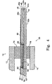
- Figures 3 and 4 illustrate an aspect of the invention wherein, as discussed above, the seal area 14 is avoided with the conduction of leads from the interior of the tube to the exterior.
- Shown in Figure 4 is a spacer 76 (see Figure 6) sealed to the face plate 12 and to the addressing grid 35.
- a spacer 78 (see Figure 6) is also seen, sealed to the back plate 16 and the addressing grid 35.
- the laminated construction of the invention adapts itself very well to making connections to the addressing grid without requiring a vacuum seal to cross over conductors.
- the layer/interface 50a is shown with a conductive trace 54, or a series of parallel traces 54 as indicated.
- the traces 54 will make contact with conductive vias 56 and 58, or series of conductive vias, comprising holes through the layers 46 and 48, filled with conductive material.
- additional traces 60 and 62 have been deposited or printed, as contact pads.
- These illustrated conductors may be used for power feed-through, such as for anode voltage, cathode power, getters and ground planes, as indicated schematically in Figure 5, at the region 64.
- the contact pads 60 and 62 comprise some of the conductors 36, 38 and 40 indicated in Figure 1. It is an important feature that the conductive traces enable high voltage or high current feed through under the seal, through use of a series of parallel traces where needed.
- Figure 3 which is a view of the addressing grid structure with the face plate 12 removed, also shows a series of leads 66, which are actually far greater in number than shown, extending as traces from columns of the holes 44. These traces 66 do not pass through the seal 14, but under the seal, continuing as external leads 68 which connect to the ASIC driver chips 20.
- the upper surface 46a of the laminated addressing grid need not be used for conductive traces; if it is used, however, conductive vias carry the conductor paths underneath the seal 14, in the manner just described with reference to power leads, in Figure 4.
- FIG. 5 is another schematic plan view showing an example of a layout for the system and electronics of the invention.
- the multilayer laminate grid structure 35 extends outside the seal 14 with at least some of the layers, as discussed above.
- ASIC drivers 20a, 20b, etc. through 20h are shown mounted on the glass ceramic laminate structure 35, near the periphery 18 of the structure outside the seal.
- Series of traces 66 and 70 may extend outwardly from the addressing grid area as indicated, and as discussed previously, these traces may be on the uppermost surface or between layers (but preferably are between layers when passing under the seal 14).
- the drawing shows layer transfer regions or interconnect regions 72 and 74, for the inter-layer conduction of traces, using conductive vias.
- Figure 6 is a sectional view of one edge of the assembly, showing the multilayer addressing grid structure 35 extending through the seal area 14. Spacers 76 and 78 are shown above and below the multilayer structure 35, with the face plate 12 above the grid structure and the back plate 16 below. A few of the supports 42 (illustrated in Figure 1) are also indicated, inboard from the spacer 76, and the spacers together hold the face plate 12 in position against the pressure created by vacuum existing in the tube. Back plate supports 51 are also visible in Figure 6, supporting the multilayer grid 35 as spaced from the back plate 16.
- Figure 6A shows an alternative structure wherein the back spacers 78 and the front spacer 76 at the seal are avoided.
- the back plate 16a is formed by a molding or casting technique, with an integral spacer comprising a boss 78a with a flat ridge 78b at the seal, at essentially the same height as the tips of the support ridges 51.
- a process for providing the back plate with supports 51 and troughs 53 is discussed in greater detail below.
- Figure 6A also shows a modified face plate 12a with an integral spacer 76a having a flat surface 76b for sealing against the grid structure 35.
- the hermetic seal is made at all interfaces around the face plate/grid/back plate assembly), preferably with solder glass 14a for sealing between the glass/ceramic and glass materials (the solder glass thickness is not to scale).
- solder glass 14a for sealing between the glass/ceramic and glass materials (the solder glass thickness is not to scale).
- solder glass thickness is not to scale.
- Figure 7 comprising Figures 7A through 7X, gives a schematic illustration of the process and formation of the multilayer grid structure 35 and of the cathode and anode and the ultimate assembly of these components.
- Figure 7A indicates one of the sheets of unfired blank glass-ceramic tape go.
- Figure 7B the punching of via holes 92 is indicated through one or more layers of the glass ceramic material 90, and this hole forming operation can be performed in accordance with a process of the invention described below with reference to Figure 8.
- the via holes are distinguished from the electron addressing holes, preferably formed at a different stage. Via holes are formed in margin area 18 and may be formed between pixel holes so as to permit interconnection of traces between layers (discussed further with reference to Figure 20, below).
- Figure 7C indicates filling of the via holes with conductive material, forming conductive vias 94.
- the via filling is accomplished by screen printing (or other types of printing) of the conductive material into the via holes, in the known manner used for multilayer ceramic circuits. This can be done, for example, using DuPont's 6141D via filling paste.
- the depositing of the conductive traces 96 on one sheet 90 of glass-ceramic material is indicated.
- the trace material specified for DuPont Green type is 6142D. This is also preferably accomplished by screen printing techniques, although other types of printing may be used.
- a drying step may follow wherein the layers are heated sufficiently to remove the volatiles from the inks of the conductive traces.
- the conductive traces 96 (which will lie in different directions on different sheets of the material) are positioned in paths where the pixel holes will be located.
- the conductive vias 94 may also have conductive traces deposited over them on some layers. As indicated, the conductive vias 94 are located in areas outside the viewing area, i.e. outside the area having the pixel holes (although in another embodiment described below, the vias are formed between and among the pixel addressing holes so as to leave the peripheral areas free for joining screen sections modularly.)
- Figure 7E indicates the step of forming the multiplicity of pixel holes 44 in the sheet 90 of unfired glass-ceramic material.
- this grid of very small holes may advantageously be formed in accordance with a hole-blowing process described below with reference to Figure 8.
- Figure 7F the series of layers 90 including layers 90a, 90b, 90c, 90d, 90e have been stacked and laminated together.
- the pixel holes 44 have been formed identically in each layer, so that they are in good registry in the resulting stack 90x. Lamination may be accomplished at this stage by a low temperature heat application, such as at about 70 C between hot platens, with pressure. This low heat is sufficient to fuse the plasticizers together between layers, so that the layers are bound together by the plasticizers.
- Figure 7F indicates conductive traces 96 running in the horizontal direction. Other traces 96a, 96b, 96c are indicated below, by successively cutaway layers at the lower left.
- Figure 7G represents another step according to a specific embodiment of the invention, whereby the multiplicity of holes 44, laid together in registry in the laminated stack of layers 90x, are treated with a flow-through of abrasive-containing fluid, preferably liquid (for example, water containing silicon carbide sub-mil particles).
- abrasive-containing fluid preferably liquid (for example, water containing silicon carbide sub-mil particles).
- This operation is conducted with a pair of opposed die plates supporting the laminated structure as explained below with reference to Figure 9.
- the pumping of abrasive-containing liquid through the pattern of holes, with the die plates on either side to channel the flow effectively reams all the holes to be sure they are the correct size and shape as desired, correcting any minor irregularities in registry among the layers, which are still plastic and unfired.
- the laminated structure is fired, in a stepped or profile firing. This may be at an initial temperature of about 350° C, in which the organics are burned out, increased in a prescribed profiling mode up to about 950° C, depending on the materials.
- the addressing grid must be supported at front and back (except for small screen embodiments), as by front supports 42 and back supports 51 engaged between the addressing grid structure 35 and the face plate 12 or the back plate 16, respectively.
- spacing support between the addressing grid and the anode or face plate a variety of techniques may be used.
- One method is to use a layer of photo-reactive glass material which is much thicker than the addressing grid structure 35 (several layers may be used).
- the addressing grid 35 can be used as a mask for exposure of the photo-reactive layers, with the W light preferably forming into a controlled diverging cone in the glass as projected through each grid hole.
- a thermal step may then be required to make the exposed volumes acid-etchable.
- the layer is then acid-etched to remove material at all areas except between addressing grid holes and therefore between pixel dots, where support is desired.
- the resulting spacer support is then thermally process to enhance its strength.
- Unfired glass ceramic tape can be used, in one thick layer or a series of stacked layers, the tape being formulated with a photolithographic characteristic.
- the photo sensitive glass ceramic tape is translucent and nearly transparent, such that the appropriate reactive light (such as ultraviolet) can pass through the spacer layer (or a series of layers separately) in the plastic, unfired state.
- the light is passed through the unfired addressing grid structure (following the step of Figure 7G, above) and into the spacer material.
- the plastic binder in the glass ceramic material changes by exposure to light, changing so as to allow it to be removed.
- the disks or cone-shaped volumes within the plastic spacer material can be removed by attacking the plastic binder material with an appropriate acid or solvent.
- the glass and/or ceramic particles wash away with the removal of the binder.
- the unfired, plastic perforated spacer sheet (or sheets) can be put together with the glass ceramic grid itself, and fired together as in the step of Figure 7H.
- Another procedure which can be used for the front spacers or spacer sheet is the earlier described process of blowing out holes through unfired glass ceramic tape.
- five sheets of unfired tape each approximately .030 inch (0.0762 x 10 -2 m) thick, can be blown out by fluid pressure using an appropriate pair of dies as described above.
- larger holes can be formed, such as for a triad of phosphor dots, i.e. one for each pixel of holes on the addressing grid. In this way the aspect ratio of material thickness to hole diameter or width can be maintained, for efficient formation of the holes with the fluid pressure process.
- the openings in the spacer sheets can be cleaned out and reamed to the correct size and shape using an abrasive liquid pumped through the holes of the spacer sheet between the dies.
- the perforated addressing grid structure may be placed at the surface of a pool of liquid, front surface down.
- the liquid is comprised of ultraviolet curable polymers, and its depth, i.e. the depth from the face of the addressing grid to the bottom of the pool, is the depth desired for the spacer sheet.
- Ultraviolet light is directed through the addressing grid holes and down into the liquid, in a manner to establish a controlled divergence of the light through the depth of the liquid.
- the liquid is not purely transmissive, helping to scatter the light into generally a cone shape.
- the result of the light exposure step is to cure the top surface of the liquid (in the event it extends slightly above the addressing grid), as well as through all of the desired hole locations and in the desired generally conical diverging shape beyond the holes.
- W curable liquids such as that manufactured by UVEXS Registered Trade Mark, Inc. of Sunnyvale, California
- no volatiles are included in the liquid material, and thus the material does not dry on exposure to air.
- the addressing grid structure is removed from the liquid bath and inverted, thus establishing a mold which can be used to produce the desired spacer sheet.
- a castable glass-ceramic material i.e. unfired glass ceramic material formulated into a castable form, is vacuum cast on the surface of the addressing grid, to a depth extending to the tips of the fine, filament-iike posts (each, for example, about 4 - 8 mils in diameter at its upper end).
- the cast material which will become the spacer sheet, sets up and then can be put in the furnace with the addressing grid and fired together with the grid.
- the cast ceramic sheet cures and its binders are burned out, shrinking to the same extent as the addressing grid (unless non-shrink ceramics are used), and the plastic filaments or columns extending through and up from the addressing grid holes are burned out.
- the amorphous glass in the glassceramic layers has fused together between layers, permanently bonding the layers into an integral, layered laminate with the conductive traces between layers and, if desired, also on one or both of the exposed front and back surfaces. If all of the conductive traces are below the surface, they are brought to the surface by the conductive vias 94, or in an alternate configuration not illustrated, the different layers can extend in stepped fashion laterally out from the seal, so that contacts associated with the conductive traces are exposed serially by layer in this way.
- the preferred embodiment is to bring all the leads to integrated circuits mounted as shown schematically in Figure 1. This advantageously utilizes the properties for which low temperature cofired ceramic tape was developed (for example, those properties listed in the Summary, above) and eliminates the need and associated costs inherent with using connectors and mounting the drive circuits remote from the display.
- Figure 7I indicates the application of solder glass 98 (similar to an ink or paint) to the front and back surfaces in a peripheral rectangular pattern at the location of the seal area 14 shown in Figure 1.
- the solder glass is pre-glazed (as also indicated in Figure 7I) by heating the laminated structure to a temperature high enough to burn off the binders and fuse the glass particles together, but low enough not to cause divitrification (for solder glass that devitrifies).
- This preglaze temperature is generally between 400°C to 600° C depending on the binder and solder glass used (see steps listed in Table III below for a preferred embodiment).
- Preglazing ensures that the binders, including organics, are cleanly burned away before the tube is sealed. This is particularly important in a high internal structure surface area to internal vacuum volume tube such as described herein, to avoid contaminants. Without preglazing, tube contamination can occur in either air or vacuum final seal due to a lack of sufficient oxygen to completely burn away the binder.
- the addressing grid 90x which may have integral supports as described above, will now be identified as the grid 35 as noted in other drawings.
- FIGS 7J through 7N indicate schematically the production of the cathode assembly, which will be assembled to the multilayer addressing grid and to the anode assembly.
- a thermionic or "hot" cathode is used.
- the cathode may be an appropriate form of cold cathode (field emitter device, FED).
- Figure 7J indicates the formation of a crenulated back plate 16b which will support the cathode and which will become the back plate 16 of the assembly.
- the sheet 16b is rigid, for example, a glass plate or a ceramic plate which has been fired (although metal alloys can be used matching the thermal coefficient of the addressing grid).
- the back plate 16b(16) and its support against the addressing grid, with the cathode structure between, can be formed in several different ways.
- the back plate can be formed of the same green tape glass ceramic material as the addressing grid as described above.
- the supports for contact with the addressing grid can be formed into the surface of the green glass ceramic material in a crenulated configuration, leaving troughs or rows of recesses within which thermionic cathode wires can be positioned, as shown in Figures 2 and 6.
- Such forming of the green tape surface can be by molding or stamping techniques. It is important that the supports be precisely positioned and of controlled and narrow dimension, since each support will form a line (or series of columns) which must contact the addressing grid between addressing holes.
- the back supports 80 are formed integrally in the front surface of the back plate 16, by molding of the unfired glass ceramic material using an appropriately formed mold.
- the shape of the troughs is cylindrical, but in other embodiments may be made non-cylindrical.
- a single cathode wire 26 can extend longitudinally through each trough formed by this method. Spacing from trough to trough can be about 200 mils, and 16 addressing grid holes 44 can be adjacent to each cathode trough.
- back plate supports 80 may be used, such as deposition of vacuum compatible materials on the back plate before or after firing, interposition of a vacuum compatible spacer web between the back plate and the addressing grid upon assembly, or other suitable techniques.
- back plate can again be a glass ceramic plate, but without supports, the supports being formed on the back surface of the addressing grid.
- the back plate can be a sheet of glass, and the supports can either be formed on the back surface of the addressing grid or deposited by a suitable process on the glass backed plate.
- Figure 7K indicates firing of the solder glass 98 on the sheet of material 16b, which may be at about 400° to 600° C as above.
- the cathode frame preferably comprises a conductive metal strip at top and bottom to which all cathode wires are secured; one or both sides preferably have spring strips (not shown) to which the cathode wire ends are secured so as to maintain tension in the wires through thermal changes.
- the spring strips in one preferred embodiment comprise chemical milled strips in a frame formed of a metal which will maintain its springy characteristic even at high temperature, for example Hastalloy B.
- Figure 7M shows a wire cathode 22, having been secured via the cathode frame 100.
- the voltage applied to the cathode wires can vary in time so that the voltage of the cathode wire adjacent to the row being addressed is near ground potential.
- the cathode wires can be run parallel to the rows and the cathode cycled on only as needed during row addressing. This approach will require that the cathode supports be electrically isolated from each other so that the cathodes can be turned on in synchronization with the row addressing.
- the cathode wires 22 are indicated as being coated with tricarbonate, a conventional procedure which may be accomplished by electrophoresis.
- Spraying is an alternative process.
- carbonates of several metals such as strontium, calcium and barium are coated onto a tungsten wire (which may be thoriated as in the known process).
- tungsten wire which may be thoriated as in the known process.
- the carbonates deposited on the cathode filaments are converted to oxides and all binding material is removed, a process well known in the industry. These steps assure that the assembled tube will have a clean cathode.
- bicarbonate mixes also give acceptable performance later forming a useful and efficient oxide cathode. This completes the back plate/cathode assembly.
- Figure 7N' shows the frame 100 with the cathode 22 removed from the back plate 16b, in exploded view for clarity (not indicating order of assembly).
- Figures 7P through 7S relate to production of the anode assembly.
- a sheet of glass 104 is applied a rectangular band of solder glass 98 (or the assembly may use a sheet of glassceramic material as described above, with glass dots embedded in holes).
- Figure 7R indicates the phosphor application process to the face plate 104.
- the phosphor dots including discrete color dots for each pixel, are preferably applied to the glass in a manner generally used for conventional video tubes such as the "photo-tacky" process.
- Photo-tacky is a process wherein a layer of material becomes tacky for a limited time when exposed to light. The phosphor powder is dusted onto the material and only sticks where the material is tacky.
- R, G and B phosphor dots for each pixel R, G and B phosphor stripes may be applied, in a known conventional manner.
- Use of a flat glass face plate allows the use of alternate methods such as offset printing to apply the phosphor material.
- the phosphor is generally indicated as 106 in Figure 7R.
- Figure 7S indicates aluminizing of the anode, i.e. covering the phosphor with a thin layer of aluminum 108, to protect and maintain the integrity of the phosphor dots and to increase the tube brightness by redirecting some of the reardirected photons toward the viewer.
- aluminization electrons must have a threshold level of energy to pierce the aluminum and excite the phosphor. This completes production of the anode/face plate 12.
- Figures 7T through 7X indicate steps in assembly of the three components together: the back plate/cathode assembly 110, the multilayer addressing grid structure 35 and the anode assembly 12.
- the preferred embodiment is carried out entirely in vacuum.
- Figure 7T indicates bakeout of the three components under vacuum
- Figure 7U shows the lamination/assembly of the three components together, producing an assembly 111.
- the tube is baked out unassembled because the high internal structure surface area as compared to internal tube volume makes conventional tabulation pumpout impractically long in production.
- solder glass seals soften and fuse together typically at 450 C for certain types of solder glass, and at times as prescribed in the material specification.
- Solder glass preglazing and sealing temperatures and times are generally specified by the glass manufacturer or are determined by the user using techniques known to those skilled in the art. Table III below gives an example for a
- Figure 7W indicates one or more getters being processed.
- a flashed getter a thin film or strip of metal (having an affinity for oxygen) is heated by electrical resistance and plated against appropriate surfaces inside the tube, such as in one or more peripheral areas of the glass ceramic grid plate, outside the active addressing area.
- Active getters can also be used, wherein the getters act as vacuum ion pumps, active whenever the tube is powered.
- Figure 7X indicates connection of the ASIC drivers 20 to the finished addressing grid structure 35, which extends outwardly from the cathode/back plate assembly 110 (16) and the anode assembly 12. This involves making electrical contact between the ASIC drivers 20 and the conductive traces, vias or busses extending along the surfaces of the peripheral areas 18 of the addressing grid structure 35.
- Figures 7A - 7X illustrate the preferred embodiment
- alternative embodiments both laminate and fire the addressing grid before forming the addressing holes (as distinguished from the via holes). Holes can then be formed by laser abrasive water jet or other drilling process, although these processes are considered less practical because of time requirements.
- 7T Vacuum Bake-Out 1. Outgas tube at 300°C until pressure stabilized at 1X10 -6 T. 2. Continue to outgas for 1 hour. 7U Assemble Tube Bring together the cathode/back plate assembly, the addressing grid and the anode/face plate for joining. 7V Seal Solder Glass 1. 300°C to 475°C at 5°C/min. 2. 475°C for 15 min. 3. 475°C to 300°C at 5°C/min. 4. 300°C for 15 min. (annealing) 5. 300°C to RT at 5°C/min. 7W Process Getter Process flash getter by application of prescribed voltage. 7X Attach ASICs Connect ASIC drivers to completed grid structure, with electrical contact to conductive traces, vias and busses.
- Shrinkage uniformity is important in producing an addressing structure and in producing an assembled CRT which is accurate and functions properly. In particular, the positions of the pixel holes must be sufficiently predictable and accurate that each hole will be in registry with and will address the appropriate phosphor dot. Most ceramic tapes exhibit some nonuniformity in shrinkage, but glass ceramic tape systems have been developed having high shrinkage and zero x-y shrinkage. Material such as DuPont 851U Green Tape has a shrinkage of 12% in x and y and 17% in z. If pressure is applied in z during firing then the x-y shrinkage can be reduced to zero while increasing the z shrinkage. Shrinkage uniformity is the variation of the shrinkage from nominal shrinkage during the firing process.
- Shrinkage uniformity is defined as the change or variation in shrinkage from the nominal value.
- 2% shrinkage uniformity about a nominal 12% shrinkage would result in the part shrinking to anywhere from 87.8% to 88.2% of its original size.
- two holes 10 inches apart in the unfired state could be located anywhere from 8.820 inches to 8.780 inches apart after firing.
- 0.01% shrinkage uniformity the range for the same example would be 8.801 inches to 8.799 inches.
- the nominal shrinkage uniformity is 0.2%.
- the preferred embodiment is to reduce the shrinkage to thereby reduce the shrinkage variation.
- the desired shrinkage uniformity is .04% for VGA level resolution and .025% for SGVA resolution.
- the shrinkage uniformity can be improved, using materials that utilize compression during firing to control shrinkage.
- each grid can be used as its own mask for photo-lithographic application of the phosphor dots, thereby eliminating any misalignment between the individual pixel holes in the grid and the corresponding phosphor dot.
- Figures 8A and 8B relate to assembly of the three main components of the cathode ray tube 10, i.e. the face plate or anode 12, the addressing grid structure 35 and back plate/cathode 110. These figures illustrate the use of alignment or registry pins 113 or 112 in holes 114, to assure proper registry of the three components upon assembly.
- Figure 8A is a plan view
- Figure 8B is a sectional view, both being schematic representations not showing all components.
- Figures 8A and 8B show two different alternatives.
- a registry pin 113 passes through a closely sized hole in the addressing grid, but into recesses 114a in the anode plate and back plate as shown, without passing through to the front and back (the back plate/cathode assembly is shown broken away at two corners in Figure 8A).
- the pins 113 are thus captured in and retained within the assembly.
- the seal 14 may be positioned outside the location of the pins 113, as shown.
- the pin 112 passes through registry holes 114 in all three components, with the pin to be removed after the assembly is complete. In this case the pins 112 are positioned outside the seal 14, since the registry holes 114 pass through the entire assembly.
- Figure 9 is a sectional view indicating a method and a die for creating the multiplicity of addressing grid holes 44 in each sheet of unfired glass ceramic material.
- the die generally indicated at 115, uses fluid pressure to blow holes through the unfired, flexible glass-ceramic material of the sheets, such as indicated in Figure 7E.
- a sheet of the material is placed at a location indicated as 116 in Figure 6, preferably between a pair of matching dies 117 and 118, each of which has a pattern of a multiplicity of bores 119, corresponding to the desired location of the pixel holes 44 for each sheet or layer of the addressing grid.
- the back die 118 is used with somewhat reduced hole quality depending on tape thickness, hole size, aspect ratio, etc.
- a pressure chamber head 120 has a fluid plenum 122 which receives fluid pressure through a pressure inlet conduit 124, as schematically indicated in the figure.
- a baffle plate or other appropriate gas-dispersing structure 125 is located between the fluid inlet and the bores 119, as shown.
- the pressure plenum 122 is sealed against the face of the first die 117, as by an O-ring peripheral seal 126.
- the pixel holes in one specific embodiment are, for example, 4 mils (10.16 x 10 -5 m) in diameter and on 13.3 mil (33.78 x 10 -5 m) pixel triad centers. They may be in a close-packed hexagonal pattern as discussed above, or a linear array of holes, slots or other shapes as desired for specific embodiments.
- the thickness of the sheet of green unfired ceramic material is an important consideration in determining the pressure necessary for forming the holes. As this thickness/diameter ratio increases, the necessary pressure rises greatly. This is also determined in part by the density of the fluid employed. Heavy gas will generally work more effectively than light gas, and liquid, with its incompressibility, can be even more effective. Experimentally it was determined, for example, that a 5 hole by 5 hole grid of 12 mil (30.48 x 10 -5 m) holes on 25 mil (63.5 x 10 -5 m) centers was easily achieved through a green glass ceramic material having a thickness of 5 mils (12.7 x 10 -5 m), using helium gas at a pressure of 2000 psi.
- This hole forming process can be enhanced by flash heating or exposing to chemicals such as MEK the glass ceramic material, only in the hole locations, prior to the pressure burst.
- the die can be used as a mask for this purpose. For example, accurate holes of 2 units have been produced through 5 mil (12.7 x 10 -5 m) tape using MEK.
- Such treatment imposed at the hole locations increases the thickness which can be punched by the hole forming process, and can enable a laminated stack of the unfired glass ceramic layers to form the holes through all layers together. The treatment reduces the pressure required to blow out the material and improves the quality of the fabricated hole.
- the hole-forming die 115 need not be large enough to form the holes for the entire display area in one step.
- the sheet of glass ceramic material may be moved to a series of different locations, all properly registered as to location relative to the die assembly 115.
- the class of materials preferred for this invention have a tendency to be of greater density toward one surface than the other. This may be due to the typical formation process wherein a tape slurry is deposited onto a plastic sheet carrier and doctor-bladed into the desired thickness. This may also be due to asymmetric evaporation of volatile materials contained in the tape slurry, ie. the volatiles can only exit from the upper surface. This movement of solvent through the tape may also transport binder to the top surface leaving the top portion of the tape binder rich. In any event, the tape material closest to the plastic sheet carrier tends to be of somewhat greater density. Recognizing this effect or characteristic of the tape material, it has been found advantageous to form the fluid-blown holes by placing the side of the tape produced on the carrier film against the upstream side of the blowing device.
- the initial rough through holes can be formed by a gang-punching technique or other mechanical means, then later abrasively cleared with the layers stacked together as described above.
- a fluid abrasive slurry can be forced through the hole columns through the stack of layers. This is preferably accomplished by again using the hole blowing die 115. With the laminated and unfired glass ceramic structure clamped between die parts 117 and 118, a fluid/abrasive slurry flowing at high speed through the bores 119 will effectively ream out the holes to the full desired diameter, correcting slight errors in registry among the layers.
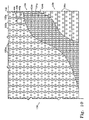
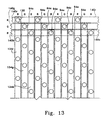
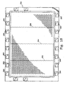
- Figures 10 through 13 illustrate structures for implementing encoding schemes in accordance with the invention, for reducing the number of leads required to address particular pixel holes, for reducing the number of drivers and for addressing the holes by rows and columns.
- conductive traces must be activated at all layers to cause electrons to pass through a particular pixel hole. ANDing of the layers enables the number of drivers to be greatly reduced.
- Figure 10 shows a portion of a three-layer laminate 130, illustrating the simplest case for a color display, without group encoding of rows and with a conductive lead required for every column and every row. ANDing is used to the extent that pixel holes are addressed by rows and columns and by the particular color (R, G or B) which must also be active for a pixel to be addressed.
- three glass-ceramic layers are included in this sample embodiment, an upper layer 132, a middle layer 134 and a bottom layer 136.
- the upper layer 132 has conductive traces 132a positioned around columns of holes 44 as shown, with gaps 132b between the conductive trace columns.
- there are groups of three holes 44r, 44g and 44b function as pixel triads in each column (example triad indicated in dashed lines).
- Column data is applied to the conductive traces 132a, preferably all columns simultaneously for a specific row, in the manner described above.
- the bottom layer 136 has conductive traces 136a to receive row data, each row comprising a row of pixels, i.e. a row of triads of holes.
- Row addressing simply comprises, in the addressing scheme contemplated herein, the selecting of each row individually and sequentially down the display, in a time-divided sequence.
- a pixel (comprising a triad of three pixel holes for color in this RGB embodiment) could be addressed uniquely by column and row. All pixels of one row can be addressed simultaneously, but with different data going to each column depending upon the input signal.
- a preferred scheme according to the invention is to time division multiplex among R, G and B while addressing a particular row in the manner described earlier. This requires inclusion of the layer 134 in which the R, G and B holes are surrounded by conductive traces 134r, 134g i and 134b as subcolumns, with the conductive interconnection of all R subcolumns, separately all G subcolumns and separately all B subcolumns.
- Figure 13 shows an arrangement for accomplishing this interconnection, using conductive vias 94a for interconnection of R subcolumns, with a conductive trace 140r serving as a connecting bar at a different level in the laminated assembly (the connective trace 140r could be on the same layer as the illustrated subcolumn traces for one color, since, as shown in Figure 10, this will not involve crossing any other subcolumn traces).
- all G subcolumn conductive traces can be connected by a conductive trace 140g at another level, and the B subcolumn conductive traces 134b, via a conductive trace 140b below.
- the connecting bars 140r, 140g and 140b can all be at a single level and that level can of course be either above or below the location of the subcolumn conductive traces.
- R data, G data and B data can be sent to the pixel holes simultaneously rather than by time division multiplexing. This will involve essentially eliminating the pixel column layer 132 and addressing the R, G and B subcolumns of the layer 134 individually, without connecting the colors together as in Figure 13. Only the layers 134 and 136 are involved. Thus, the time duration of activation of each pixel hole is tripled, tripling brightness. However, the number of column leads is tripled, thereby tripling the number of drivers required since R, G and B data is being sent simultaneously.
- Figure 12 is a simplified timing signal diagram for a color display addressing grid.
- the diagram indicates that the entire row, Row N in this example, is activated for certain unit of time (for example, 1/30 second). This interval is indicated at 145.
- the drawing indicates column data being applied, with time division between R, G and B data.
- Column data can be applied with R data from maximum potential interval 146 (dashed lines) which is equal to one-third of the total row interval 145.
- Dashed lines 147 show the division of the interval 145 into thirds. Examples are indicated in which, for columns 1, 2 and 3, R data is applied for respective intervals 148, 150 and 152. These intervals depend on the brightness specified for the R dot in each pixel of the row.
- G column data is shown being applied for potentially the next one-third of the total row duration 145, with different G intervals 154, 156 and 158 being applied for the example pixels (columns) 1, 2 and 3.
- B data is applied for the remaining onethird of the row interval 145, in the manner described for R and G data.
- Figure 11 illustrates an example of row encoding.
- binary encoding is advantageously employed; however, quaternary or octal or 16 division or higher encoding can be used to reduce the number of layers if desired.
- Encoding is achieved by ANDing of a series of layers 166, 167, 168, 170, 172 and 174, the latter being the column data layer.
- a single conductive trace 166a surrounds all the A pixel holes on the layer 166 as shown, while a single conductive trace 166b surrounds all the pixel holes in the second half of the display area or B area.
- the first area (over or under 166a) is divided into A and B and the second area (over or under 166b) is also divided into A and B sections.
- the layer is thus divided into four quarters, with the A conductive traces wired together and the B conductive traces wired together (connections not shown).
- each section is further divided into an A and B section, and again all A traces at this level are wired together and all B traces at this level are wired together (connections not shown).
- the sections are again divided, now with 16 different rows of traces, again dividing the sections of the layer immediately above/below each into A and B sections.
- a further division is shown at the next layer 172.
- the layer 172 is shown divided down to the individual pixels, but in practice there will be many times the 32 rows illustrated, requiring several more layers.
- the required number of layers can be reduced by the use of higher order encoding division on some layers, such as quaternary, octal or 16-lead division. This encoding has the additional advantage of reducing the capacitance per division. This is desirable to insure the required drive current is within low cost driver capability.
- the row traces receive a signal consisting of AAAAB, for example (for the layers 166, 168, 167, 170 and 172, respectively), this will activate the second row from the top in Figure 11. If the signal is BABBA, this will activate the lowermost row seen in Figure 11.
- FIG 11A is a schematic, greatly enlarged cross section of a portion of an addressing grid according to the invention, showing six layers 181 through 186, and the interlayer conductive traces which form rings around the pixel hole 44.
- conductive traces 181a, 182a, 183a, 184a and 185a are shown only between layers, but as discussed above, the traces can be applied at either of the top and bottom surfaces of the grid assembly.
- the traces closest to the cathode will experience a lower cut-off voltage, the voltage necessary to repel all electrons, than will the traces closest to the anode.
- the required current, i is given by CV/t, where C is the trace capacitance, V is the desired voltage and t is the time to charge the trace. For a given charge time, capacitance, and resistance, the power goes as the square of the required voltage. It is therefore important that the fastest changing signals be applied to the traces closest to the cathode where the required voltage is lowest and the necessary power is thus minimized.
- the lowest conductive traces 181a can be for column data, as in the traces 174 of the monochrome example of Figure 11.
- the next four layers above can carry four levels of row encoding, i.e. at the traces 182a, 183a, 184a and 185a. The encoding which requires the fastest switching should be done at the lowest voltage as indicated above.
- the top level row encoding, at the traces 185a should have the fewest traces (e.g. only two as in Figure 11).
- grey code techniques which are well known
- Grey code techniques reduce the number of layers of conductive traces which must be changed in transitioning from one row to another.
- Grey code minimizes the number of transitions in encoding levels, thereby minimizing the required power. Grey codes are no more difficult to mechanically encode in the multilayer ceramic than any other encoding scheme, such as the discussed binary encoding, octal encoding, etc.
- conductive traces or a sheet-like conductive layer can be placed on the top surface of the upper layer 186, or this conductive layer can be below the top surface (traces not shown in Figure 11A).
- Such a conductive layer located as the closest conductive layer to the anode, shields the switching region from electric fields produced by the anode voltage. This also will further modify the field lines inside the addressing holes 44, to reduce the voltage necessary to turn on and off the gate. This is important in that, in some configurations, a relatively high switching voltage is required to switch the last element of the addressing hole gate, i.e. the uppermost conductive trace 185a shown in Figure 11A.
- conductive traces or a conductive layer, in order to help accelerate electrons through the grid.
- This layer improves the extraction of electrons from the cathode and aids in making the electron flow more uniform.
- a cathode-side layer on the grid acts as a sink for power, but it can improve the performance of the cathode ray tube by providing a higher density of electrons to the back side of the grid.
- FIG 11B shows an alternative embodiment of an encoded grid structure 165a by which brightness of the display can be doubled through activating two rows of pixels at a time.
- the display is shown as monochrome, with the addressing holes in simple orthogonal rows and columns, but it should be understood that this arrangement is particularly advantageous in a color display, where brightness is more often critical.
- the addressing grid is divided in half at a horizontal dividing line 176 at which the column traces are discontinuous.
- the top half, 176a, and the bottom half, 176b, of each column are fed different data, simultaneously.
- the top row of pixels of the top half, 176a is preferably activated at the same time as the top row of pixels of the lower half, 176b.
- two parallel horizontal lines are traced down the screen simultaneously, and brightness is doubled.
- each column in a row receives different data at one time, and in the doubled-brightness embodiment, each column receives two sets of data, an upper set and a lower set.
- this brightness-doubling arrangement can be used with other possible arrangements for increasing brightness.
- the individual colors such as R, G and B
- the change in color driving can increase brightness by a factor of three.
- the double row driving which can alternatively be triple, quadruple, etc. row driving
- brightness can be increased by a factor of six.
- Figures 14A and 14B show alternatives for forming conductive traces around pixel holes, depending on density required.
- screen printing techniques are limited in accuracy and resolution.
- conductive traces 134r, 134g and 134b become very close together and limits may be reached as to accuracy of very fine widths of the traces and of the spaces between them.
- the traces are illustrated side by side, with color subcolumns R, G, B, R, G, B occurring in succession.
- an alternative made possible by the multilayer addressing grid structure of the invention is to place R traces alone on one layer (not shown).
- G traces and B traces are on different layers, and, as described above, all R traces can be interconnected, as well as all G traces and all B traces. In this case the R traces can be connected directly at the same level, since no G traces or B traces will be crossed, and the case is similar with the G traces and B traces.
- Figure 14b Another alternative, illustrated in Figure 14b, is to alternate by locating every second subcolumn of conductive traces on a given layer. This will require two layers for R, G and B color selection, rather than three. Such an arrangement requires traces for all three colors to appear on each of the two layers, but the Rs are easily interconnected by conductive vias and traces, and the same with the Gs and Bs.
- Figure 14b shows a layer with an R trace 190r, no trace at the adjacent G subcolumn, then a B trace 190b. The R subcolumn is then skipped, and next appears a G trace 190g.
- Each of two layers thus has R, G and B traces.
- Figure 15 shows schematically, in a partial sectional view, a juncture or joint 210 between a pair of addressing grid modules 212 and 214.
- An overall plan view of a modularized addressing grid structure 216 formed in this way is shown in Figure 16.
- each addressing grid module 212 and 214 preferably have notched or serrated areas 218, for assuring proper registry between the modules and the rows of the addressing grid upon assembly.
- the seal area 220 which extends around the pair of assembled modules near their periphery, is notched by a recess or notch 222, formed on each module and extending from the exterior edge to a position 224 which is within the band defined by the seal area 220.
- This notching provides a means for application of the glass frit sealing material not only to the upper surfaces of the modules for sealing to the anode and back plate, but also for direct application to the facing surfaces where the two modules 212 and 214 meet at the edge, within the notch (perpendicular to plane of Figure 15). In this way a secure seal is assured between the facing surfaces.
- FIG 16 shows that the two end type modules 212 and 214 still leave space for transfer areas 226 and 228 at left and right, one on each module 212 and 214.
- drivers 230 handle the addressing of pixels on each respective side of the assembly, with these two sets of drivers appropriately synchronized.
- the flexibility in design afforded by the multilayer grid allows the modules to be constructed so that no traces need to cross between the mating modules. In this way the modules need only align mechanically.
- FIG 17 shows a series of modules, illustrated as three modules 232, 234 and 236, making up a display 238.
- the center module 234 has no left and right margins for location of trace transfers to the periphery of the display assembly 238, i.e. no transfer areas similar to the areas 226 and 228 on end modules. Connections between the row traces and the drives must be made entirely on an individual module. This requires the use of conductive vias placed between the pixel holes and interconnecting traces to connect the row traces to one or more) transfer layers (discussed below with reference to Figure 19). From the transfer layer the conductive path can be taken to drivers 240 at top and bottom of the assembly. The drivers 240 are connected with drivers on the end modules 232 and 236, for synchronized operation of the row traces, as well as of the column traces and color select traces.
- interpixel vias generally is only necessary for display designs where multiple modules are necessary. Those displays would typically be large displays (over 25 inch diagonal) where the interpixel spacing is large, allowing sufficient room for such via designs. For small displays, where the space between pixels is more limited, these vias would normally not be necessary.
- Figure 18 is a plan view of a display assembly 250 which comprises a single module, rather than joined module sections.
- Figure 18 illustrates the principle that the electronics can nonetheless be modular within the display, in the case of a very large display 250.
- Vertical dividing lines 252, 254 and 256 are shown in dashed lines in Figure 18, to indicate that the horizontal traces are divided into four sections as far as driving electronics are concerned. In very long conductive traces, problems of capacitance and resistance will be encountered, adversely affecting the electron transfer and the operation of the display.
- a multiple printing scheme is used to divide each horizontal trace into multiple sections, such as four for the embodiment shown in Figure 18.
- Each section along a trace line is driven separately, but in coordination, via connected drive electronics 260. Again, interpixel conductive vias are used to bring the trace sections down to one or more transfer layers, since no margin is available at the divisions 252, 254 and 256 for bringing the traces out to the edges.
- Figure 19 is a greatly enlarged schematic view showing interpixel conductive vias 262.
- Conductive traces in the form described above relative to Figures 14A and 14B, for example, are shown at 264.
- the interpixel conductive vias 262 which may be considerably smaller than the addressing holes 44, are placed at locations where the printed conductive traces 264 can be separated a reasonable distance without losing any substantial portion of the conductive path.
- Figure 20 shows a portion of a curved screen embodiment of the invention.
- the curved, thin screen display 266 is similar in dimensions and proportions to the embodiments described above, but it is curved concavely relatively to the viewer, for specialized applications such as simulators, targeting applications for combat, or special effects for use with a very large screen.
- the screen display may also be curved convexly for certain display applications.
- the illustrated components are similar to those described earlier.
- Figure 21 shows another variation of the invention.
- a portion of a two-sided thin CRT display 270 is shown, with two separate addressing grids 35 but a common cathode 272 which supplies electrons in both directions, for each anode/faceplate 12.
- a screen can be circular, for example, as in a radar screen, or irregular so as to fit into a vehicle dashboard or an aircraft control panel.
- Grids need not have addressing holes laid out on an orthogonal basis, but can be arranged by polar coordinates. In a circular screen, for example, holes can be on radial lines, with traces following radial lines and others in concentric circles.
- FIG 22 is a block diagram schematically indicating drive electronics for a flat screen display in accordance with the invention.
- the video signal is shown at 300 entering the analog separator 302 where it is divided out into the red, green and blue (R, G and B) components of video signal.
- the red, green and blue components are digitized by analog to digital converters 304, 306 and 308 as shown.
- Each of the red, green and blue components of the video signal is digitized in its own A to D digitizer 304, 306 and 308.
- the video signal is a digital signal rather than an analog signal, the signal would be impressed at points to the right of the A/D converters in the drawing, without the analog separation and A/D converters being used.
- the digitized video signals, red, green and blue, are passed through storage registers 310, 312 and 314. Following the red path, the signal goes through a two-way switch 316 into one of two registers 320 or 322. Two register counters are used; one is loaded while the other is being outputted to the MUX for display. The register counters are loaded in serial fashion, otherwise known as a -bucket brigade", filling from the left to the right until all column data is stored. Once the register counters are filled, they are switched through the two-way switch 324 into the multiplexer or MUX 330. This is identical to the process which is carried out for the green and the blue signals, via register counters 326 and 328.
- the original video signal provided a sync pulse 333 which goes through sync generator 334 and comes out as a clock signal 335 which is used to drive both the register counters for loading the digital data into the counters, and another output 335a of the sync generator provides signals to a divider/encoder 336.
- the output of the divider/encoder 336 is used to drive the row select line 340.
- the analog separator 302 provides output signals 341 to drive both the multiplexer 330 and the display RGB select lines 342. In this way the same synchronized selection signal coordinates the MUX's selection of either R, G or B data while simultaneously selecting the appropriate R, G or B select lines within the glass/ceramic grid. Therefore, when the MUX has been selected to transmit R data to the display columns, only the red phosphor dots in each column are active because only the red select lines have been activated.
- the analog signal is separated into its component colors which pass through A/D converters to storage registers and finally are impressed one row at a time onto the columns of the display 35 while simultaneously counters have divided down the row information and impressed that on the row select and the color select data at the appropriate times.
- hole is intended to encompass not only circular holes, but also slot-shaped holes, elliptical holes, hexagonal holes, triangular holes; or any other shape which might be appropriate for a particular application or selected arrangement of the addressing grid and the pixels. Differently shaped holes are appropriate to different types of screens and also to the number of colors selected in a color complement for a pixel. If four-color pixels are selected, square-shaped or diamond-shaped holes may be preferred.
- red, green, and blue colors are referred to in the above description, this is not intended to limit the invention in this aspect, and four-color pixels may alternatively be used.
- plastic is sometimes used herein in its technical sense of meaning workable or deformable in a non-elastic way.
- glass-ceramic or “ceramic” is often used herein to refer to the family of glass, ceramic, glass-ceramic, or ceramic glass materials as described earlier. This is particularly true in reference to ceramic tapes, a term used frequently in the claims.
- screening printing is often mentioned.
- the reference to screen printing is intended broadly, and should be understood to include lithography, flat plate printing techniques, and other printing techniques.
- Lithography can actually achieve a greater density of conductive traces since, in general, 1/4 micron resolution can be achieved, far higher resolution than screen printing.
Landscapes
- Engineering & Computer Science (AREA)
- Manufacturing & Machinery (AREA)
- Cathode-Ray Tubes And Fluorescent Screens For Display (AREA)
- Vessels, Lead-In Wires, Accessory Apparatuses For Cathode-Ray Tubes (AREA)
Abstract
Claims (14)
- Dispositif électronique (10) comprenant une structure d'adressage (35) destiné à commander le passage d'électrons à travers des ouvertures dans une structure à grille, la structure d'adressage (35) comprenant :un empilement solidairement fusionné de couches diélectriques (46, 48, 50, 52) comportant des trous (44) s'étendant à travers l'empilement, des couches diélectriques adjacentes étant directement liées pour être sensiblement indiscernables individuellement dans l'empilement, etdes traces conductrices (54) formées sur une surface d'au moins certaines des couches diélectriques (46, 48, 50, 52) comprenant une portion d'une trace conductrice adjacente à chaque trou, de sorte que la portion de la trace conductrice adjacente à chaque trou puisse produire un champ électrique pour gouverner le passage d'électrons à travers ce trou.
- Dispositif électronique (10) selon la revendication 1, dans lequel les couches diélectriques (46, 48, 50, 52) sont fusionnées ensemble par soudage par diffusion.
- Dispositif électronique (10) selon la revendication 1, dans lequel les couches diélectriques (46, 48, 50, 52) comprennent des couches en céramique fusionnées ensemble par soudage de verre entre les couches en céramique.
- Dispositif électronique (10) selon la revendication 1, dans lequel la structure d'adressage (35) est une partie d'un tube à vide, le dispositif électronique comprenant en outre :une plaque frontale (12) en tant que frontière externe du tube à vide, etune pluralité de pixels fluorescents sur la surface intérieure de la plaque frontale (12), chaque pixel comprenant un complément d'éléments fluorescents, chaque trou différent à travers la structure d'adressage (35) étant adjacent à un élément fluorescent correspondant pour adresser respectivement et séparément chaque élément fluorescent de chaque pixel.
- Dispositif électronique (10) selon la revendication 1, dans lequel la structure d'adressage (35) est une partie d'un tube à vide, le dispositif électronique comprenant en outre :une plaque frontale (12) en tant que frontière externe formée d'une feuille de verre,une substance fluorescente formée sur la surface interne de la plaque frontale (12), etun moyen espaceur (42, 76, 78) situé sur l'empilement des couches diélectriques (46, 48, 50, 52) et faisant saillie de la surface d'une couche externe parmi les couches diélectriques, entre les trous (44), pour fournir une série de supports contre lesquels la plaque frontale (12) se met en prise.
- Dispositif électronique (10) selon la revendication 1, dans lequel la structure d'adressage (35) est une partie d'un ensemble de tube cathodique, le dispositif électronique comprenant en outre :une plaque frontale (12) en tant que frontière externe,une substance fluorescente formée sur la surface interne de la plaque frontale (12),une plaque arrière (16) derrière la structure d'adressage (35),une cathode (22) entre la plaque arrière (16) et la structure d'adressage (35), etun moyen d'obturation (14a, 98) pour obturer hermétiquement l'ensemble.
- Dispositif électronique (10) selon la revendication 6, dans lequel les couches diélectriques (46, 48, 50, 52) sont formées d'un matériau de verre-céramique initialement non mis à feu et flexible qui est mis à feu après que les couches sont stratifiées ensemble, les couches de verre-céramique étant fusionnées ensemble par la mise à feu via un soudage de verre entre les couches de verre-céramique.
- Dispositif électronique (10) selon la revendication 1, dans lequel la structure d'adressage (35) est une partie d'un tube à vide qui met en oeuvre un écran à tube cathodique plat, le dispositif électronique comprenant en outre :une plaque frontale (12) en tant que frontière externe du tube à vide,une plaque arrière (16) derrière la structure d'adressage (35),une cathode (22) entre la plaque arrière (16) et la structure d'adressage (35),un moyen d'obturation hermétique (14a, 98) situé le long d'une zone d'obturation périphérique entre la structure d'adressage (35) et la plaque arrière (16) et entre la structure d'adressage et la plaque frontale (12), la structure d'adressage comprenant une zone de marge périphérique s'étendant à l'extérieur de la zone d'obturation, etdes pilotes d'ASIC (20) montés sur la zone de marge périphérique de la structure d'adressage (35) et connectés de manière appropriée auxdites traces conductrices (54).
- Dispositif électronique (10) selon la revendication 1, dans lequel la structure d'adressage (35) est une partie d'un écran plat, le dispositif électronique comprenant en outre :un moyen de cathode (22) généralement à l'arrière de l'écran plat pour établir une source d'électrons dans une disposition généralement plane, etun moyen de grille d'adressage adjacent à et en face du moyen de cathode (22), le moyen de grille d'adressage comprenant :(a) la structure d'adressage, chaque trou correspondant à un pixel excitable par électron, les traces conductrices (54) permettant à chaque pixel d'être adressé individuellement en appliquant une tension à une portion de la trace conductrice adjacente au pixel, et(b) un moyen pour connecter les traces conductrices (54) à l'extérieur de la structure d'adressage (35) de sorte que des tensions puissent être appliquées aux traces conductrices depuis l'extérieur de la structure d'adressage, etun moyen de plaque frontale (12) en face du moyen de grille d'adressage, ledit moyen de plaque frontale ayant une surface frontale et une surface arrière, la surface arrière portant les pixels, ledit moyen de plaque frontale étant positionné adjacent aux trous (44) pour recevoir des électrons accélérés contre la surface arrière du moyen de plaque frontale par le moyen de grille d'adressage pour amener chaque pixel à briller lorsqu'il est excité par des électrons.
- Dispositif électronique (10) selon la revendication 1, dans lequel chaque trou comporte une paroi interne ayant, en différentes profondeurs à travers le trou, des conducteurs électriques (36, 38, 40) exposés au trou, et dans lequel certaines des traces conductrices (44) mènent de chacun des conducteurs exposés (36, 38, 40) à des emplacements extérieurs à la structure d'adressage (35), des traces conductrices différentes parmi les traces conductrices (54) étant à différents niveaux dans la structure d'adressage (35), moyennant quoi différentes tensions peuvent être appliquées aux conducteurs électriques différents parmi les conducteurs électriques en chaque trou (44) pour établir des champs électriques qui soit feront passer des électrons, soit empêcheront le passage d'électrons.
- Dispositif électronique (10) selon la revendication 1, dans lequel :les couches diélectriques (46, 48, 50, 52) sont formées d'un matériau de verre-céramique initialement non mis à feu et flexible ;les couches de verre-céramique sont stratifiées ensemble pour former une structure multicouche ;les trous (44) sont formés à travers la structure multicouche en des emplacements souhaités ; etla structure multicouche est mise à feu de façon à fusionner ensemble les couches de verre-céramique.
- Dispositif électronique (10) selon la revendication 1, dans lequel :les couches (46, 48, 50, 52) sont formées d'un matériau de verre-céramique initialement non mis à feu et flexible ;les trous (44) sont formés à travers chacune des couches de verre-céramique (46, 48, 50, 52) en des emplacements souhaités,les couches de verre-céramique (46, 48, 50, 52) sont stratifiées ensemble pour former une structure multicouche de telle sorte que les trous (44) des diverses couches sont coïncidant ;la structure multicouche est mise à feu pour fusionner ensemble les couches de verre-céramique (46, 48, 50, 52).
- Procédé de production d'une structure de grille d'adressage (35) destinée à commander le mouvement des électrons vers une plaque frontale fluorescente (12) dans un écran à tube cathodique plat, le procédé comprenant les étapes consistant à :former des traces métalliques (54) sur une série de couches (46, 48, 50, 52) de matériau en feuille flexible, en effectuant l'une des étapes suivantes consistant à(a) stratifier les couches (46, 48, 50, 52) en une structure multicouche de telle sorte que certaines des traces métalliques reposent entre les couches,(b) fournir une multiplicité de trous (44) à travers chacune des couches (46, 48, 50, 52), les trous étant coïncidents de façon à coïncider avec les traces métalliques (54) et de façon à avoir des traces conductrices entourant sensiblement au moins une majorité des trous (44), et(c) soumettre la structure stratifiée multicouche à un traitement spécifié pour convertir la structure stratifiée multicouche en une structure rigide et compatible avec le vide dans laquelle les couches (46, 48, 50, 52) sont solidairement fusionnées ensemble de façon à être sensiblement indiscernables individuellement, en effectuant une autre des étapes de stratification, de formation de trous et de soumission à un traitement, eteffectuer la troisième des étapes de stratification, de formation de trous et de soumission à un traitement à l'étape de stratification qui est effectuée avant l'étape de soumission à un traitement.
- Procédé de formation d'un motif précis de petits trous (44) dans une structure stratifiée multicouche qui a des traces conductrices inter-couches (54), le procédé comprenant les étapes consistant à :former des trous traversants non finis (44) dans chacune d'une série de couches de bandes initialement plastiques, soit collectivement, soit individuellement, qui formeront la structure stratifiée multicouche, en utilisant une filière sur n'importe quel côté des emplacements des trous et en appliquant une pression de fluide sur un côté pour éliminer un matériau par soufflage pour former chaque trou traversant, etavec les couches (46, 48, 50, 52) empilées ensemble et stratifiées, mais encore à l'état plastique, et avec le motif des trous (44) généralement coïncidant, faire passer un fluide comprenant un matériau abrasif à travers chaque trou traversant non fini de l'empilement stratifié, avec une filière à chaque côté de l'empilement définissant la taille souhaitée de chaque trou de façon à ce qu'un fluide passe au travers, nettoyant ainsi et agrandissant les trous, éliminant les bords rugueux, établissant une coïncidence précise de trous à travers l'empilement des couches et assurant que tout court-circuit involontaire entre le matériau des traces conductrices sur différentes couches soit éliminé.
Applications Claiming Priority (3)
| Application Number | Priority Date | Filing Date | Title |
|---|---|---|---|
| US07/867,044 US5424605A (en) | 1992-04-10 | 1992-04-10 | Self supporting flat video display |
| US867044 | 1992-04-10 | ||
| PCT/US1993/003057 WO1993021650A1 (fr) | 1992-04-10 | 1993-04-08 | Ecran de visualisation plat autoporteur |
Publications (3)
| Publication Number | Publication Date |
|---|---|
| EP0635162A1 EP0635162A1 (fr) | 1995-01-25 |
| EP0635162A4 EP0635162A4 (fr) | 1997-04-16 |
| EP0635162B1 true EP0635162B1 (fr) | 2006-09-27 |
Family
ID=25348959
Family Applications (1)
| Application Number | Title | Priority Date | Filing Date |
|---|---|---|---|
| EP93911573A Expired - Lifetime EP0635162B1 (fr) | 1992-04-10 | 1993-04-08 | Ecran de visualisation plat autoporteur |
Country Status (5)
| Country | Link |
|---|---|
| US (7) | US5424605A (fr) |
| EP (1) | EP0635162B1 (fr) |
| AU (1) | AU4045493A (fr) |
| DE (1) | DE69334065T2 (fr) |
| WO (1) | WO1993021650A1 (fr) |
Families Citing this family (216)
| Publication number | Priority date | Publication date | Assignee | Title |
|---|---|---|---|---|
| US5675212A (en) | 1992-04-10 | 1997-10-07 | Candescent Technologies Corporation | Spacer structures for use in flat panel displays and methods for forming same |
| CN1026943C (zh) * | 1990-03-06 | 1994-12-07 | 杭州大学 | 平板彩色显示器 |
| US5859508A (en) * | 1991-02-25 | 1999-01-12 | Pixtech, Inc. | Electronic fluorescent display system with simplified multiple electrode structure and its processing |
| CA2073923C (fr) | 1991-07-17 | 2000-07-11 | Hidetoshi Suzuki | Dispositif de formation d'images |
| US5424605A (en) * | 1992-04-10 | 1995-06-13 | Silicon Video Corporation | Self supporting flat video display |
| US5903098A (en) * | 1993-03-11 | 1999-05-11 | Fed Corporation | Field emission display device having multiplicity of through conductive vias and a backside connector |
| US5686790A (en) * | 1993-06-22 | 1997-11-11 | Candescent Technologies Corporation | Flat panel device with ceramic backplate |
| BE1007780A3 (nl) * | 1993-11-25 | 1995-10-17 | Philips Electronics Nv | Beeldweergeefinrichting met een platte vacuümbuis. |
| GB2285168B (en) * | 1993-12-22 | 1997-07-16 | Marconi Gec Ltd | Electron field emission devices |
| JP3671429B2 (ja) * | 1994-02-22 | 2005-07-13 | ソニー株式会社 | 画像表示装置および画像表示駆動方法 |
| US5731228A (en) * | 1994-03-11 | 1998-03-24 | Fujitsu Limited | Method for making micro electron beam source |
| JP2800879B2 (ja) * | 1994-06-21 | 1998-09-21 | 富士通株式会社 | 蛍光表示装置及びその駆動方法 |
| FR2724041B1 (fr) * | 1994-08-24 | 1997-04-11 | Pixel Int Sa | Ecran plat de visualisation a haute tension inter-electrodes |
| WO1996008833A1 (fr) * | 1994-09-15 | 1996-03-21 | Panocorp Display Systems, Inc. | Systeme de visualisation fluorescent electronique a structure d'electrodes multiples simplifiee et procede de fabrication |
| US5658832A (en) * | 1994-10-17 | 1997-08-19 | Regents Of The University Of California | Method of forming a spacer for field emission flat panel displays |
| US5646702A (en) * | 1994-10-31 | 1997-07-08 | Honeywell Inc. | Field emitter liquid crystal display |
| US5612256A (en) * | 1995-02-10 | 1997-03-18 | Micron Display Technology, Inc. | Multi-layer electrical interconnection structures and fabrication methods |
| US5766053A (en) * | 1995-02-10 | 1998-06-16 | Micron Technology, Inc. | Internal plate flat-panel field emission display |
| JP2852357B2 (ja) * | 1995-03-09 | 1999-02-03 | 双葉電子工業株式会社 | 表示装置 |
| JP3083076B2 (ja) * | 1995-04-21 | 2000-09-04 | キヤノン株式会社 | 画像形成装置 |
| WO1997008730A1 (fr) * | 1995-08-25 | 1997-03-06 | International Business Machines Corporation | Dispositif d'affichage |
| US5697825A (en) * | 1995-09-29 | 1997-12-16 | Micron Display Technology, Inc. | Method for evacuating and sealing field emission displays |
| CN1202974A (zh) | 1995-10-26 | 1998-12-23 | 图象技术公司 | 冷阴极场致发射体平面屏幕显示器 |
| DE69615666T2 (de) * | 1995-12-18 | 2002-08-01 | Koninklijke Philips Electronics N.V., Eindhoven | Kanalplatte mit aus organischem material bestehenden wänden für eine plasmagesteuerte anzeigevorrichtung sowie verfahren zur herstellung einer solchen platte |
| US5697827A (en) * | 1996-01-11 | 1997-12-16 | Rabinowitz; Mario | Emissive flat panel display with improved regenerative cathode |
| US5844359A (en) * | 1996-01-18 | 1998-12-01 | Micron Display Technology, Inc. | Lightweight back plate for FED and flat CRT vacuum envelopes |
| US5804920A (en) * | 1996-01-19 | 1998-09-08 | Philips Electronics North America Corporation | Plasma addressed liquid crystal display with etched glass spacers |
| KR100377066B1 (ko) * | 1996-01-30 | 2003-06-18 | 사르노프 코포레이션 | 플라즈마디스플레이와그제조방법 |
| US5893967A (en) * | 1996-03-05 | 1999-04-13 | Candescent Technologies Corporation | Impedance-assisted electrochemical removal of material, particularly excess emitter material in electron-emitting device |
| US5766446A (en) * | 1996-03-05 | 1998-06-16 | Candescent Technologies Corporation | Electrochemical removal of material, particularly excess emitter material in electron-emitting device |
| US5710483A (en) * | 1996-04-08 | 1998-01-20 | Industrial Technology Research Institute | Field emission device with micromesh collimator |
| FR2748348B1 (fr) * | 1996-05-06 | 1998-07-24 | Pixtech Sa | Ecran couleur a micropointes a double grille |
| US5726529A (en) * | 1996-05-28 | 1998-03-10 | Motorola | Spacer for a field emission display |
| RU2115194C1 (ru) * | 1996-07-04 | 1998-07-10 | Михаил Евгеньевич Гиваргизов | Электронно-оптическая система, матричная электронно-оптическая система, устройства на их основе (варианты) |
| KR200164860Y1 (ko) * | 1996-07-16 | 2000-01-15 | 윤종용 | 모니터 케이스의 사출금형 게이트랜딩구조 |
| US6049165A (en) * | 1996-07-17 | 2000-04-11 | Candescent Technologies Corporation | Structure and fabrication of flat panel display with specially arranged spacer |
| US5859502A (en) * | 1996-07-17 | 1999-01-12 | Candescent Technologies Corporation | Spacer locator design for three-dimensional focusing structures in a flat panel display |
| US5898266A (en) | 1996-07-18 | 1999-04-27 | Candescent Technologies Corporation | Method for displaying frame of pixel information on flat panel display |
| JPH10149778A (ja) * | 1996-09-17 | 1998-06-02 | Toshiba Corp | 微小冷陰極管とその駆動方法 |
| US5831382A (en) * | 1996-09-27 | 1998-11-03 | Bilan; Frank Albert | Display device based on indirectly heated thermionic cathodes |
| US5947783A (en) * | 1996-11-01 | 1999-09-07 | Si Diamond Technology, Inc. | Method of forming a cathode assembly comprising a diamond layer |
| US5973452A (en) * | 1996-11-01 | 1999-10-26 | Si Diamond Technology, Inc. | Display |
| FR2756417A1 (fr) * | 1996-11-22 | 1998-05-29 | Pixtech Sa | Ecran plat de visualisation a grilles focalisatrices |
| US5864205A (en) * | 1996-12-02 | 1999-01-26 | Motorola Inc. | Gridded spacer assembly for a field emission display |
| US6109994A (en) | 1996-12-12 | 2000-08-29 | Candescent Technologies Corporation | Gap jumping to seal structure, typically using combination of vacuum and non-vacuum environments |
| US5977706A (en) * | 1996-12-12 | 1999-11-02 | Candescent Technologies Corporation | Multi-compartment getter-containing flat-panel device |
| US5820435A (en) * | 1996-12-12 | 1998-10-13 | Candescent Technologies Corporation | Gap jumping to seal structure including tacking of structure |
| US6139390A (en) * | 1996-12-12 | 2000-10-31 | Candescent Technologies Corporation | Local energy activation of getter typically in environment below room pressure |
| US5964630A (en) * | 1996-12-23 | 1999-10-12 | Candescent Technologies Corporation | Method of increasing resistance of flat-panel device to bending, and associated getter-containing flat-panel device |
| US5888112A (en) * | 1996-12-31 | 1999-03-30 | Micron Technology, Inc. | Method for forming spacers on a display substrate |
| GB2321335A (en) * | 1997-01-16 | 1998-07-22 | Ibm | Display device |
| US5994828A (en) * | 1997-02-10 | 1999-11-30 | U.S. Philips Corporation | Picture display device with addressing system |
| GB2322471A (en) * | 1997-02-24 | 1998-08-26 | Ibm | Self stabilising cathode |
| US6114802A (en) * | 1997-02-28 | 2000-09-05 | Motorola, Inc. | Field emission device having stamped substrate and method |
| JP3234188B2 (ja) | 1997-03-31 | 2001-12-04 | キヤノン株式会社 | 画像形成装置とその製造方法 |
| JP3703287B2 (ja) | 1997-03-31 | 2005-10-05 | キヤノン株式会社 | 画像形成装置 |
| US6140767A (en) * | 1997-04-25 | 2000-10-31 | Sarnoff Corporation | Plasma display having specific substrate and barrier ribs |
| US6046539A (en) * | 1997-04-29 | 2000-04-04 | Candescent Technologies Corporation | Use of sacrificial masking layer and backside exposure in forming openings that typically receive light-emissive material |
| US6154188A (en) * | 1997-04-30 | 2000-11-28 | Candescent Technologies Corporation | Integrated metallization for displays |
| MY129516A (en) | 1997-05-30 | 2007-04-30 | Toshiba Kk | Image display apparatus and method of manufacturing the same |
| US6129603A (en) * | 1997-06-24 | 2000-10-10 | Candescent Technologies Corporation | Low temperature glass frit sealing for thin computer displays |
| US5872424A (en) * | 1997-06-26 | 1999-02-16 | Candescent Technologies Corporation | High voltage compatible spacer coating |
| US6120674A (en) * | 1997-06-30 | 2000-09-19 | Candescent Technologies Corporation | Electrochemical removal of material in electron-emitting device |
| US6111351A (en) | 1997-07-01 | 2000-08-29 | Candescent Technologies Corporation | Wall assembly and method for attaching walls for flat panel display |
| US6200181B1 (en) * | 1997-07-01 | 2001-03-13 | Candescent Technologies Corporation | Thermally conductive spacer materials and spacer attachment methods for thin cathode ray tube |
| US6356013B1 (en) * | 1997-07-02 | 2002-03-12 | Candescent Intellectual Property Services, Inc. | Wall assembly and method for attaching walls for flat panel display |
| US6169358B1 (en) | 1997-07-11 | 2001-01-02 | Emagin Corporation | Method and apparatus for flashover control, including a high voltage spacer for parallel plate electron beam array devices and method of making thereof |
| US6354897B1 (en) * | 1997-08-25 | 2002-03-12 | Raytheon Company | Field emission displays and manufacturing methods |
| US6147664A (en) * | 1997-08-29 | 2000-11-14 | Candescent Technologies Corporation | Controlling the brightness of an FED device using PWM on the row side and AM on the column side |
| KR19990029275A (ko) * | 1997-09-11 | 1999-04-26 | 맥그라스 달린 에스 | 평면 디스플레이 장치 |
| GB9720723D0 (en) * | 1997-10-01 | 1997-11-26 | Screen Developments Ltd | Visual Display |
| RU2000111546A (ru) * | 1997-10-01 | 2002-08-10 | Комплит Дисплей Солушнз Лимитед (Gb) | Индикатор изображения |
| IT1295366B1 (it) * | 1997-10-20 | 1999-05-12 | Getters Spa | Sistema getter per pannelli piatti al plasma impiegati come schermi |
| TW392186B (en) * | 1997-12-01 | 2000-06-01 | Hitachi Ltd | Plasma display panel and image display using the same |
| US6046541A (en) * | 1997-12-15 | 2000-04-04 | Motorola, Inc. | Flat panel display having a random spacer arrangement |
| US6249083B1 (en) * | 1998-01-12 | 2001-06-19 | Samsung Display Devices Co., Ltd. | Electric field emission display (FED) and method of manufacturing spacer thereof |
| US5990613A (en) * | 1998-01-20 | 1999-11-23 | Motorola, Inc. | Field emission device having a non-coated spacer |
| US6040809A (en) * | 1998-01-30 | 2000-03-21 | Candescent Technologies Corporation | Fed display row driver with chip-to-chip settling time matching and phase detection circuits used to prevent uneven or nonuniform brightness in display |
| US6067061A (en) * | 1998-01-30 | 2000-05-23 | Candescent Technologies Corporation | Display column driver with chip-to-chip settling time matching means |
| US6004830A (en) * | 1998-02-09 | 1999-12-21 | Advanced Vision Technologies, Inc. | Fabrication process for confined electron field emission device |
| US6168737B1 (en) | 1998-02-23 | 2001-01-02 | The Regents Of The University Of California | Method of casting patterned dielectric structures |
| US6153075A (en) | 1998-02-26 | 2000-11-28 | Micron Technology, Inc. | Methods using electrophoretically deposited patternable material |
| US5990614A (en) * | 1998-02-27 | 1999-11-23 | Candescent Technologies Corporation | Flat-panel display having temperature-difference accommodating spacer system |
| US6949289B1 (en) | 1998-03-03 | 2005-09-27 | Ppg Industries Ohio, Inc. | Impregnated glass fiber strands and products including the same |
| US6419981B1 (en) | 1998-03-03 | 2002-07-16 | Ppg Industries Ohio, Inc. | Impregnated glass fiber strands and products including the same |
| US6593255B1 (en) | 1998-03-03 | 2003-07-15 | Ppg Industries Ohio, Inc. | Impregnated glass fiber strands and products including the same |
| US8105690B2 (en) | 1998-03-03 | 2012-01-31 | Ppg Industries Ohio, Inc | Fiber product coated with particles to adjust the friction of the coating and the interfilament bonding |
| US6107731A (en) * | 1998-03-31 | 2000-08-22 | Candescent Technologies Corporation | Structure and fabrication of flat-panel display having spacer with laterally segmented face electrode |
| US6888146B1 (en) * | 1998-04-10 | 2005-05-03 | The Regents Of The University Of California | Maskless micro-ion-beam reduction lithography system |
| US6113450A (en) | 1998-05-14 | 2000-09-05 | Candescent Technologies Corporation | Seal material frit frame for flat panel displays |
| US6174449B1 (en) | 1998-05-14 | 2001-01-16 | Micron Technology, Inc. | Magnetically patterned etch mask |
| JPH11329310A (ja) * | 1998-05-20 | 1999-11-30 | Futaba Corp | アクティブマトリクス駆動蛍光表示管及びその製造方法 |
| US6051937A (en) * | 1998-05-29 | 2000-04-18 | Candescent Technologies Corporation | Voltage ratio regulator circuit for a spacer electrode of a flat panel display screen |
| US6031336A (en) * | 1998-06-17 | 2000-02-29 | Motorola, Inc. | Field emission display and method for the operation thereof |
| KR100459948B1 (ko) * | 1998-06-18 | 2005-02-28 | 삼성에스디아이 주식회사 | 전계방출표시소자 |
| US6414428B1 (en) | 1998-07-07 | 2002-07-02 | Candescent Technologies Corporation | Flat-panel display with intensity control to reduce light-centroid shifting |
| US6140759A (en) * | 1998-07-17 | 2000-10-31 | Sarnoff Corporation | Embossed plasma display back panel |
| US6147665A (en) * | 1998-09-29 | 2000-11-14 | Candescent Technologies Corporation | Column driver output amplifier with low quiescent power consumption for field emission display devices |
| US6137213A (en) * | 1998-10-21 | 2000-10-24 | Motorola, Inc. | Field emission device having a vacuum bridge focusing structure and method |
| US6617772B1 (en) | 1998-12-11 | 2003-09-09 | Candescent Technologies Corporation | Flat-panel display having spacer with rough face for inhibiting secondary electron escape |
| US6403209B1 (en) | 1998-12-11 | 2002-06-11 | Candescent Technologies Corporation | Constitution and fabrication of flat-panel display and porous-faced structure suitable for partial or full use in spacer of flat-panel display |
| US6352763B1 (en) | 1998-12-23 | 2002-03-05 | 3M Innovative Properties Company | Curable slurry for forming ceramic microstructures on a substrate using a mold |
| US6247986B1 (en) | 1998-12-23 | 2001-06-19 | 3M Innovative Properties Company | Method for precise molding and alignment of structures on a substrate using a stretchable mold |
| US6533632B1 (en) * | 1999-02-18 | 2003-03-18 | Micron Technology, Inc. | Method of evacuating and sealing flat panel displays and flat panel displays using same |
| JP2000306532A (ja) * | 1999-04-22 | 2000-11-02 | Futaba Corp | 多重アノードマトリックス方式蛍光表示管、およびその駆動装置 |
| US7071907B1 (en) | 1999-05-07 | 2006-07-04 | Candescent Technologies Corporation | Display with active contrast enhancement |
| US6064145A (en) * | 1999-06-04 | 2000-05-16 | Winbond Electronics Corporation | Fabrication of field emitting tips |
| US6756729B1 (en) * | 1999-08-23 | 2004-06-29 | Samsung Sdi Co., Ltd. | Flat panel display and method of fabricating same |
| KR100312690B1 (ko) * | 1999-08-25 | 2001-11-03 | 김순택 | 형광표시관 |
| JP4345153B2 (ja) * | 1999-09-27 | 2009-10-14 | ソニー株式会社 | 映像表示装置の製造方法 |
| US6710525B1 (en) | 1999-10-19 | 2004-03-23 | Candescent Technologies Corporation | Electrode structure and method for forming electrode structure for a flat panel display |
| US6570322B1 (en) * | 1999-11-09 | 2003-05-27 | Micron Technology, Inc. | Anode screen for a phosphor display with a plurality of pixel regions defining phosphor layer holes |
| AU3268601A (en) * | 1999-11-15 | 2001-05-30 | Mesa Vision | Monolithic multi-electrode grid structures for application in thin flat cathode ray array tubes |
| US6429596B1 (en) | 1999-12-31 | 2002-08-06 | Extreme Devices, Inc. | Segmented gate drive for dynamic beam shape correction in field emission cathodes |
| US6555025B1 (en) | 2000-01-31 | 2003-04-29 | Candescent Technologies Corporation | Tuned sealing material for sealing of a flat panel display |
| TW472285B (en) * | 2000-03-17 | 2002-01-11 | Acer Display Tech Inc | Plasma display panel with tight sealing between two plates and the manufacturing method thereof |
| WO2001071760A1 (fr) * | 2000-03-23 | 2001-09-27 | Kabushiki Kaisha Toshiba | Ensemble espaceur pour afficheur a surface plane, procede de fabrication de cet ensemble espaceur, procede de fabrication d'afficheur a surface plane, afficheur a surface plane et moule utilisable dans le cadre de la fabrication de l'ensemble espaceur |
| TW509960B (en) * | 2000-04-04 | 2002-11-11 | Matsushita Electric Industrial Co Ltd | Highly productive method of producing plasma display panel |
| US6246177B1 (en) | 2000-04-28 | 2001-06-12 | Motorola, Inc. | Partial discharge method for operating a field emission display |
| US6441559B1 (en) | 2000-04-28 | 2002-08-27 | Motorola, Inc. | Field emission display having an invisible spacer and method |
| JP2002082652A (ja) * | 2000-05-18 | 2002-03-22 | Canon Inc | 画像表示装置および方法 |
| US7064500B2 (en) * | 2000-05-26 | 2006-06-20 | Exaconnect Corp. | Semi-conductor interconnect using free space electron switch |
| US6407516B1 (en) | 2000-05-26 | 2002-06-18 | Exaconnect Inc. | Free space electron switch |
| US6800877B2 (en) * | 2000-05-26 | 2004-10-05 | Exaconnect Corp. | Semi-conductor interconnect using free space electron switch |
| US6801002B2 (en) * | 2000-05-26 | 2004-10-05 | Exaconnect Corp. | Use of a free space electron switch in a telecommunications network |
| US6545425B2 (en) | 2000-05-26 | 2003-04-08 | Exaconnect Corp. | Use of a free space electron switch in a telecommunications network |
| US6800232B2 (en) * | 2000-05-31 | 2004-10-05 | Ttm Advanced Circuits, Inc. | PCB support plate method for PCB via fill |
| US6821178B2 (en) | 2000-06-08 | 2004-11-23 | 3M Innovative Properties Company | Method of producing barrier ribs for plasma display panel substrates |
| US6716078B1 (en) | 2000-07-27 | 2004-04-06 | Motorola Inc. | Field emission display and method of manufacture |
| US6722937B1 (en) | 2000-07-31 | 2004-04-20 | Candescent Technologies Corporation | Sealing of flat-panel device |
| JP2002063864A (ja) * | 2000-08-21 | 2002-02-28 | Ise Electronics Corp | 蛍光表示管 |
| US6577057B1 (en) | 2000-09-07 | 2003-06-10 | Motorola, Inc. | Display and method of manufacture |
| US6620012B1 (en) | 2000-10-27 | 2003-09-16 | Science Applications International Corporation | Method for testing a light-emitting panel and the components therein |
| US6762566B1 (en) | 2000-10-27 | 2004-07-13 | Science Applications International Corporation | Micro-component for use in a light-emitting panel |
| US6801001B2 (en) | 2000-10-27 | 2004-10-05 | Science Applications International Corporation | Method and apparatus for addressing micro-components in a plasma display panel |
| US6796867B2 (en) | 2000-10-27 | 2004-09-28 | Science Applications International Corporation | Use of printing and other technology for micro-component placement |
| US7288014B1 (en) | 2000-10-27 | 2007-10-30 | Science Applications International Corporation | Design, fabrication, testing, and conditioning of micro-components for use in a light-emitting panel |
| US6822626B2 (en) | 2000-10-27 | 2004-11-23 | Science Applications International Corporation | Design, fabrication, testing, and conditioning of micro-components for use in a light-emitting panel |
| US6935913B2 (en) | 2000-10-27 | 2005-08-30 | Science Applications International Corporation | Method for on-line testing of a light emitting panel |
| US6545422B1 (en) | 2000-10-27 | 2003-04-08 | Science Applications International Corporation | Socket for use with a micro-component in a light-emitting panel |
| US6612889B1 (en) | 2000-10-27 | 2003-09-02 | Science Applications International Corporation | Method for making a light-emitting panel |
| US6764367B2 (en) | 2000-10-27 | 2004-07-20 | Science Applications International Corporation | Liquid manufacturing processes for panel layer fabrication |
| US6570335B1 (en) | 2000-10-27 | 2003-05-27 | Science Applications International Corporation | Method and system for energizing a micro-component in a light-emitting panel |
| US6879162B2 (en) * | 2000-11-07 | 2005-04-12 | Sri International | System and method of micro-fluidic handling and dispensing using micro-nozzle structures |
| US6798131B2 (en) * | 2000-11-20 | 2004-09-28 | Si Diamond Technology, Inc. | Display having a grid electrode with individually controllable grid portions |
| US6714017B2 (en) * | 2000-11-30 | 2004-03-30 | Candescent Technologies Corporation | Method and system for infrared detection of electrical short defects |
| JP3762871B2 (ja) * | 2001-03-02 | 2006-04-05 | 双葉電子工業株式会社 | 電子管 |
| WO2002089169A1 (fr) * | 2001-04-23 | 2002-11-07 | Kabushiki Kaisha Toshiba | Afficheur d'images, procede et dispositif de production de l'afficheur d'images |
| US7081928B2 (en) * | 2001-05-16 | 2006-07-25 | Hewlett-Packard Development Company, L.P. | Optical system for full color, video projector using single light valve with plural sub-pixel reflectors |
| US6758711B2 (en) * | 2001-06-14 | 2004-07-06 | Hewlett-Packard Development Company, L.P. | Integrated focusing emitter |
| US6741016B2 (en) | 2001-06-14 | 2004-05-25 | Hewlett-Packard Development Company, L.P. | Focusing lens for electron emitter with shield layer |
| US6822628B2 (en) | 2001-06-28 | 2004-11-23 | Candescent Intellectual Property Services, Inc. | Methods and systems for compensating row-to-row brightness variations of a field emission display |
| JP2003031125A (ja) * | 2001-07-17 | 2003-01-31 | Toshiba Corp | 平面表示装置に用いるスペーサアッセンブリの製造方法 |
| US6554673B2 (en) | 2001-07-31 | 2003-04-29 | The United States Of America As Represented By The Secretary Of The Navy | Method of making electron emitters |
| JP2003109524A (ja) * | 2001-09-27 | 2003-04-11 | Toshiba Corp | 画像表示装置 |
| US6742257B1 (en) * | 2001-10-02 | 2004-06-01 | Candescent Technologies Corporation | Method of forming powder metal phosphor matrix and gripper structures in wall support |
| US7176492B2 (en) * | 2001-10-09 | 2007-02-13 | 3M Innovative Properties Company | Method for forming ceramic microstructures on a substrate using a mold and articles formed by the method |
| US7033534B2 (en) * | 2001-10-09 | 2006-04-25 | 3M Innovative Properties Company | Method for forming microstructures on a substrate using a mold |
| WO2004049287A1 (fr) * | 2001-10-31 | 2004-06-10 | Sri International | Systeme et procede de gestion et de distribution de microfluides au moyen de structures de microbuses |
| FR2834122B1 (fr) * | 2001-12-20 | 2004-04-02 | Thales Sa | Procede de fabrication d'electrodes et tube electronique a vide utilisant ce procede |
| US6659323B2 (en) * | 2002-01-30 | 2003-12-09 | Presstek, Inc. | Methods and apparatus for prescribing web tracking in processing equipment |
| JP3877294B2 (ja) * | 2002-02-13 | 2007-02-07 | 松下電器産業株式会社 | 冷陰極カソードの駆動方法および冷陰極カソード |
| US7381283B2 (en) | 2002-03-07 | 2008-06-03 | Yageo Corporation | Method for reducing shrinkage during sintering low-temperature-cofired ceramics |
| KR20030079270A (ko) * | 2002-04-03 | 2003-10-10 | 삼성에스디아이 주식회사 | 전계 방출 표시소자와 이의 제조장치 및 제조방법 |
| JP3977128B2 (ja) * | 2002-04-15 | 2007-09-19 | キヤノン株式会社 | 記録システム |
| US6909427B2 (en) * | 2002-06-10 | 2005-06-21 | Koninklijke Philips Electronics N.V. | Load adaptive column driver |
| KR100463190B1 (ko) * | 2002-06-12 | 2004-12-23 | 삼성에스디아이 주식회사 | 금속 메쉬 일체형 스페이서 구조체 및 이 구조체를 갖는평판 표시 소자 |
| EP1378347A1 (fr) * | 2002-07-01 | 2004-01-07 | Yageo Corporation | Procédé pour la diminution du retrait au frittage de céramiques cuités a basse température |
| US6771027B2 (en) * | 2002-11-21 | 2004-08-03 | Candescent Technologies Corporation | System and method for adjusting field emission display illumination |
| JP3655281B2 (ja) * | 2002-12-19 | 2005-06-02 | 双葉電子工業株式会社 | 蛍光発光管 |
| KR100459906B1 (ko) * | 2002-12-26 | 2004-12-03 | 삼성에스디아이 주식회사 | 전계방출표시소자 및 그 제조방법 |
| JP2004241159A (ja) * | 2003-02-03 | 2004-08-26 | Futaba Corp | 蛍光発光管 |
| US8062746B2 (en) | 2003-03-10 | 2011-11-22 | Ppg Industries, Inc. | Resin compatible yarn binder and uses thereof |
| US6781319B1 (en) | 2003-04-11 | 2004-08-24 | Motorola, Inc. | Display and method of manufacture |
| JP4133586B2 (ja) * | 2003-05-23 | 2008-08-13 | Tdk株式会社 | 平面パネルディスプレイ用スペーサ基材、平面パネルディスプレイ用スペーサ基材の製造方法、平面パネルディスプレイ用スペーサ、及び、平面パネルディスプレイ |
| JP3769292B2 (ja) * | 2003-07-16 | 2006-04-19 | 双葉電子工業株式会社 | 蛍光発光管 |
| JP2007534138A (ja) * | 2003-07-22 | 2007-11-22 | イエダ リサーチ アンド ディベロプメント カンパニー リミテッド | 電子放出装置 |
| JP4133675B2 (ja) * | 2003-08-19 | 2008-08-13 | Tdk株式会社 | 平面パネルディスプレイ用スペーサ、平面パネルディスプレイ用スペーサの製造方法、及び、平面パネルディスプレイ |
| TWI278887B (en) * | 2003-09-02 | 2007-04-11 | Ind Tech Res Inst | Substrate for field emission display |
| US7053558B2 (en) * | 2003-09-03 | 2006-05-30 | Sri International | System and method for controlling emission by a micro-fabricated charge-emission device |
| DE10343073A1 (de) * | 2003-09-17 | 2005-04-21 | Patent Treuhand Ges Fuer Elektrische Gluehlampen Mbh | Verfahren zur Herstellung einer flachen Entladungslampe mit Abstandselementen |
| US20050099127A1 (en) * | 2003-11-12 | 2005-05-12 | Kuo-Ming Chen | Light emitting panel module |
| CN100342479C (zh) * | 2003-11-26 | 2007-10-10 | 三星Sdi株式会社 | 平板显示器 |
| KR20050051532A (ko) * | 2003-11-27 | 2005-06-01 | 삼성에스디아이 주식회사 | 전계방출 표시장치 |
| TW200535901A (en) * | 2004-02-17 | 2005-11-01 | Tdk Corp | Method for producing spacer for flat panel display |
| US20050189164A1 (en) * | 2004-02-26 | 2005-09-01 | Chang Chi L. | Speaker enclosure having outer flared tube |
| KR20050104641A (ko) * | 2004-04-29 | 2005-11-03 | 삼성에스디아이 주식회사 | 전자 방출 표시장치 |
| CN1725922A (zh) * | 2004-07-22 | 2006-01-25 | 清华大学 | 场发射平面光源装置及其阴极 |
| CN1728329A (zh) * | 2004-07-30 | 2006-02-01 | 清华大学 | 光源装置 |
| US7354641B2 (en) | 2004-10-12 | 2008-04-08 | Ppg Industries Ohio, Inc. | Resin compatible yarn binder and uses thereof |
| US20060086020A1 (en) * | 2004-10-27 | 2006-04-27 | Eastman Kodak Company | Multi-mode flat-panel light-emitting sign |
| KR100601990B1 (ko) * | 2005-02-07 | 2006-07-18 | 삼성에스디아이 주식회사 | 전계방출 표시장치 및 그 제조방법 |
| US20070001579A1 (en) * | 2005-06-30 | 2007-01-04 | Eun-Suk Jeon | Glass-to-glass joining method using laser, vacuum envelope manufactured by the method, electron emission display having the vacuum envelope |
| US20070024170A1 (en) * | 2005-07-26 | 2007-02-01 | Kang Jung-Ho | Vacuum envelope and electron emission display device including the same |
| JP2007112950A (ja) * | 2005-10-24 | 2007-05-10 | Canon Inc | 蛍光体材料及びこれを用いた発光部材、画像表示装置 |
| TWI305859B (en) * | 2005-11-23 | 2009-02-01 | Chunghwa Picture Tubes Ltd | Planar light source and method for fabricating thereof |
| WO2007096986A1 (fr) * | 2006-02-24 | 2007-08-30 | Ibiden Co., Ltd. | Dispositif de chauffage de face d'extremite, procede de sechage de la face d'extremite d'un assemblage en nid d'abeille et procede de production de structures en nid d'abeille |
| TWI334154B (en) | 2006-05-19 | 2010-12-01 | Samsung Sdi Co Ltd | Light emission device and display device |
| US20090015132A1 (en) * | 2007-07-10 | 2009-01-15 | Kuei-Wen Cheng | Leading means of electrode leads of field emission display |
| GB0719747D0 (en) * | 2007-10-10 | 2007-11-21 | Materialise Nv | Method and apparatus for automatic support generation for an object made by means of a rapid prototype production method |
| JP2009140655A (ja) * | 2007-12-04 | 2009-06-25 | Canon Inc | 電子放出素子、電子源、画像表示装置および電子放出素子の製造方法 |
| CN101452797B (zh) * | 2007-12-05 | 2011-11-09 | 清华大学 | 场发射电子源及其制备方法 |
| KR100913179B1 (ko) * | 2008-01-09 | 2009-08-20 | 삼성에스디아이 주식회사 | 발광 장치 및 이 발광 장치를 광원으로 사용하는 표시 장치 |
| US20090250246A1 (en) * | 2008-04-07 | 2009-10-08 | Andrew Yaung | Solder by numbers, a method and system for populating printed circuit boards |
| US8802203B2 (en) | 2011-02-22 | 2014-08-12 | Guardian Industries Corp. | Vanadium-based frit materials, and/or methods of making the same |
| US9290408B2 (en) | 2011-02-22 | 2016-03-22 | Guardian Industries Corp. | Vanadium-based frit materials, and/or methods of making the same |
| US9309146B2 (en) | 2011-02-22 | 2016-04-12 | Guardian Industries Corp. | Vanadium-based frit materials, binders, and/or solvents and methods of making the same |
| KR20120139391A (ko) * | 2011-06-17 | 2012-12-27 | 삼성전자주식회사 | 게터 룸에 포스트가 구비된 전계방출패널 |
| US20140137910A1 (en) * | 2012-11-20 | 2014-05-22 | Bratney Companies | Dry ice blasting cleaning system and method of using the same |
| US9988302B2 (en) | 2014-02-04 | 2018-06-05 | Guardian Glass, LLC | Frits for use in vacuum insulating glass (VIG) units, and/or associated methods |
| US9593527B2 (en) | 2014-02-04 | 2017-03-14 | Guardian Industries Corp. | Vacuum insulating glass (VIG) unit with lead-free dual-frit edge seals and/or methods of making the same |
| CN111344489B (zh) * | 2017-07-11 | 2023-05-16 | 斯坦福研究院 | 紧凑型静电离子泵 |
| CN109980400B (zh) * | 2017-12-28 | 2021-07-23 | 泰科电子(上海)有限公司 | 连接器 |
| CN109982504B (zh) * | 2017-12-28 | 2021-06-25 | 泰科电子(上海)有限公司 | 电路板和板卡 |
| JP7653867B2 (ja) * | 2021-08-25 | 2025-03-31 | 株式会社東芝 | 熱電子発電素子及び熱電子発電モジュール |
| CN117080294B (zh) * | 2023-07-07 | 2024-02-13 | 江苏澄擎新能源有限公司 | 一种光伏面板自动化生产用层叠设备 |
Family Cites Families (83)
| Publication number | Priority date | Publication date | Assignee | Title |
|---|---|---|---|---|
| US3303374A (en) * | 1961-01-17 | 1967-02-07 | Litton Prec Products Inc | Cathode ray tube including face plate comprising tapered fiber optical elements mounted in an opaque mosaic |
| US3237039A (en) * | 1961-04-17 | 1966-02-22 | Litton Prec Products Inc | Cathode ray tube using fiber optics faceplate |
| US3228275A (en) * | 1963-04-22 | 1966-01-11 | Taber Philip | Punch and die assembly |
| US3330707A (en) * | 1963-10-07 | 1967-07-11 | Varian Associates | Method for reducing electron multipactor on a dielectric window surface |
| US3566187A (en) * | 1968-10-09 | 1971-02-23 | Wagner Electric Corp | Phosphorescent display tube having x-y signal grids and control circuitry for same |
| US3612944A (en) * | 1969-06-30 | 1971-10-12 | Northrop Corp | Electron beam scanner having plural coded dynode electrodes |
| US3622828A (en) * | 1969-12-01 | 1971-11-23 | Us Army | Flat display tube with addressable cathode |
| US3755704A (en) * | 1970-02-06 | 1973-08-28 | Stanford Research Inst | Field emission cathode structures and devices utilizing such structures |
| US3789471A (en) * | 1970-02-06 | 1974-02-05 | Stanford Research Inst | Field emission cathode structures, devices utilizing such structures, and methods of producing such structures |
| US3654505A (en) * | 1970-06-05 | 1972-04-04 | Motorola Inc | Black enamel glass for cathode-ray tube |
| US3753022A (en) * | 1971-04-26 | 1973-08-14 | Us Army | Miniature, directed, electron-beam source |
| JPS4889678A (fr) * | 1972-02-25 | 1973-11-22 | ||
| FR2243589A5 (en) * | 1973-09-11 | 1975-04-04 | Centre Techn Ind Mecanique | Method of punching holes in metal sheet - uses fluid press. applied against sheet lying over apertured matrix |
| DE2412869C3 (de) * | 1974-03-18 | 1980-10-30 | Siemens Ag, 1000 Berlin Und 8000 Muenchen | Anzeigevorrichtung mit einem Gasentladungsraum als Elektronenquelle, mit einem Elektronennachbeschleunigungsraum und mit einem Leuchtschirm und Verfahren zum Betrieb dieser Anzeigevorrichtung |
| FR2269194A1 (en) * | 1974-04-25 | 1975-11-21 | Texas Instruments Inc | Scanner for charged particle beam - has two electrodes behind particle generator with interdigitated electrode segments |
| US3936697A (en) * | 1974-04-25 | 1976-02-03 | Texas Instruments Incorporated | Charged particle beam scanning device |
| US3922420A (en) * | 1974-05-31 | 1975-11-25 | Rca Corp | Method of making a semi-transparent photomask |
| US4020381A (en) * | 1974-12-09 | 1977-04-26 | Texas Instruments Incorporated | Cathode structure for a multibeam cathode ray tube |
| US3935499A (en) * | 1975-01-03 | 1976-01-27 | Texas Instruments Incorporated | Monolythic staggered mesh deflection systems for use in flat matrix CRT's |
| US4075535A (en) * | 1975-04-15 | 1978-02-21 | Battelle Memorial Institute | Flat cathodic tube display |
| US4088920A (en) * | 1976-03-29 | 1978-05-09 | Rca Corporation | Flat display device with beam guide |
| US4174523A (en) * | 1976-07-16 | 1979-11-13 | Rca Corporation | Flat display device |
| US4227117A (en) * | 1978-04-28 | 1980-10-07 | Matsuhita Electric Industrial Co., Ltd. | Picture display device |
| GB2031220B (en) * | 1978-10-04 | 1983-01-06 | English Electric Valve Co Ltd | Evacuated display tubes |
| EP0025221B1 (fr) * | 1979-09-05 | 1983-06-29 | Kabushiki Kaisha Toshiba | Dispositif de visualisation plat |
| US4292862A (en) * | 1979-09-12 | 1981-10-06 | Owens-Corning Fiberglas Corporation | Method and apparatus for production of a stream feeder |
| DE3036671A1 (de) * | 1980-09-29 | 1982-05-13 | Siemens AG, 1000 Berlin und 8000 München | Flacher bildschirm, verfahren zu seiner herstellung und seine verwendung |
| DE3112200A1 (de) * | 1981-03-27 | 1982-10-14 | Siemens AG, 1000 Berlin und 8000 München | Flache bildwiedergaberoehre und ihre verwendung |
| US4728851A (en) * | 1982-01-08 | 1988-03-01 | Ford Motor Company | Field emitter device with gated memory |
| DE3202782A1 (de) * | 1982-01-28 | 1983-08-04 | Siemens AG, 1000 Berlin und 8000 München | Verfahren und vorrichtung zum lochen von flaechenhaften erzeugnissen |
| DE3222850A1 (de) * | 1982-06-18 | 1983-12-22 | Siemens AG, 1000 Berlin und 8000 München | Flache elektronenstrahlroehre mit einer gasentladung als elektronenquelle |
| US4531122A (en) * | 1982-07-14 | 1985-07-23 | Redfield Lawrence J | Flatscreen |
| US4618801A (en) * | 1983-01-10 | 1986-10-21 | Mitsuteru Kakino | Flat cathode ray tube |
| NL8302966A (nl) * | 1983-08-25 | 1985-03-18 | Philips Nv | Beeldweergeefpaneel. |
| US4577133A (en) * | 1983-10-27 | 1986-03-18 | Wilson Ronald E | Flat panel display and method of manufacture |
| US4685998A (en) * | 1984-03-22 | 1987-08-11 | Thomson Components - Mostek Corp. | Process of forming integrated circuits with contact pads in a standard array |
| FR2568394B1 (fr) * | 1984-07-27 | 1988-02-12 | Commissariat Energie Atomique | Dispositif de visualisation par cathodoluminescence excitee par emission de champ |
| JPS61224256A (ja) * | 1985-03-28 | 1986-10-04 | Mitsubishi Electric Corp | 平板状光源 |
| JPS625343U (fr) * | 1985-03-29 | 1987-01-13 | ||
| GB2174535B (en) * | 1985-04-29 | 1989-07-05 | Philips Electronic Associated | Display tube |
| US4719388A (en) * | 1985-08-13 | 1988-01-12 | Source Technology Corporation | Flat electron control device utilizing a uniform space-charge cloud of free electrons as a virtual cathode |
| JPS62147635A (ja) * | 1985-12-20 | 1987-07-01 | Matsushita Electric Ind Co Ltd | 表示装置 |
| IT1188132B (it) * | 1986-05-07 | 1987-12-30 | Fameccanica Spa | Procedimento e dispositivo per la produzione di film perforati particolarmente film perforati di materiale plastico per articoli igienico sanitari |
| US4994708A (en) * | 1986-07-01 | 1991-02-19 | Canon Kabushiki Kaisha | Cold cathode device |
| US4820661A (en) * | 1986-07-15 | 1989-04-11 | E. I. Du Pont De Nemours And Company | Glass ceramic dielectric compositions |
| US4948759A (en) * | 1986-07-15 | 1990-08-14 | E. I. Du Pont De Nemours And Company | Glass ceramic dielectric compositions |
| US4857799A (en) * | 1986-07-30 | 1989-08-15 | Sri International | Matrix-addressed flat panel display |
| US5015912A (en) * | 1986-07-30 | 1991-05-14 | Sri International | Matrix-addressed flat panel display |
| FR2604823B1 (fr) * | 1986-10-02 | 1995-04-07 | Etude Surfaces Lab | Dispositif emetteur d'electrons et son application notamment a la realisation d'ecrans plats de television |
| US4887000A (en) * | 1986-11-06 | 1989-12-12 | Sushita Electric Industrial Co., Ltd. | Electron beam generation apparatus |
| EP0278038A1 (fr) * | 1987-02-13 | 1988-08-17 | Battelle-Institut e.V. | Ecran de visualisation actif plat |
| US4904895A (en) * | 1987-05-06 | 1990-02-27 | Canon Kabushiki Kaisha | Electron emission device |
| FR2623013A1 (fr) * | 1987-11-06 | 1989-05-12 | Commissariat Energie Atomique | Source d'electrons a cathodes emissives a micropointes et dispositif de visualisation par cathodoluminescence excitee par emission de champ,utilisant cette source |
| US4867935A (en) * | 1988-02-26 | 1989-09-19 | E. I. Du Pont De Nemours And Company | Method for preparing ceramic tape compositions |
| US4874981A (en) * | 1988-05-10 | 1989-10-17 | Sri International | Automatically focusing field emission electrode |
| JP2630988B2 (ja) * | 1988-05-26 | 1997-07-16 | キヤノン株式会社 | 電子線発生装置 |
| US4924148A (en) * | 1988-06-24 | 1990-05-08 | Tektronix, Inc. | High brightness panel display device |
| US5063327A (en) * | 1988-07-06 | 1991-11-05 | Coloray Display Corporation | Field emission cathode based flat panel display having polyimide spacers |
| US4923421A (en) * | 1988-07-06 | 1990-05-08 | Innovative Display Development Partners | Method for providing polyimide spacers in a field emission panel display |
| EP0364964B1 (fr) * | 1988-10-17 | 1996-03-27 | Matsushita Electric Industrial Co., Ltd. | Cathodes à émission de champ |
| US5003219A (en) * | 1988-11-10 | 1991-03-26 | Matsushita Electric Industrial Co., Ltd. | Fixed construction for plate electrodes in a flat display unit |
| FR2641412B1 (fr) * | 1988-12-30 | 1991-02-15 | Thomson Tubes Electroniques | Source d'electrons du type a emission de champ |
| NL9000060A (nl) * | 1989-06-01 | 1991-01-02 | Philips Nv | Beeldweergeefinrichting van het dunne type. |
| US4978952A (en) * | 1989-02-24 | 1990-12-18 | Collimated Displays Incorporated | Flat screen color video display |
| NL8901075A (nl) * | 1989-04-28 | 1990-11-16 | Philips Nv | Inrichting ten behoeve van elektronengeneratie en weergeefinrichting. |
| US5227691A (en) * | 1989-05-24 | 1993-07-13 | Matsushita Electric Industrial Co., Ltd. | Flat tube display apparatus |
| US5160871A (en) * | 1989-06-19 | 1992-11-03 | Matsushita Electric Industrial Co., Ltd. | Flat configuration image display apparatus and manufacturing method thereof |
| DE69009307T3 (de) * | 1989-06-19 | 2004-08-26 | Matsushita Electric Industrial Co., Ltd., Kadoma | Anzeigevorrichtung mit flachem Bildschirm. |
| US4956574A (en) * | 1989-08-08 | 1990-09-11 | Motorola, Inc. | Switched anode field emission device |
| EP0436997B1 (fr) * | 1990-01-10 | 1996-03-27 | Koninklijke Philips Electronics N.V. | Dispositif de reproduction d'image du type mince |
| US4964946A (en) * | 1990-02-02 | 1990-10-23 | The United States Of America As Represented By The Secretary Of The Navy | Process for fabricating self-aligned field emitter arrays |
| JPH0614454B2 (ja) * | 1990-03-22 | 1994-02-23 | 松下電子工業株式会社 | シャドウマスク型カラー受像管 |
| NL9001529A (nl) * | 1990-07-05 | 1992-02-03 | Philips Nv | Beeldweergeefinrichting van het dunne type. |
| FR2663462B1 (fr) * | 1990-06-13 | 1992-09-11 | Commissariat Energie Atomique | Source d'electrons a cathodes emissives a micropointes. |
| US5130614A (en) * | 1990-08-08 | 1992-07-14 | Massachusetts Institute Of Technology | Ribbon beam cathode ray tube |
| US5057047A (en) * | 1990-09-27 | 1991-10-15 | The United States Of America As Represented By The Secretary Of The Navy | Low capacitance field emitter array and method of manufacture therefor |
| NL9100122A (nl) * | 1991-01-25 | 1992-08-17 | Philips Nv | Weergeefinrichting. |
| US5229691A (en) * | 1991-02-25 | 1993-07-20 | Panocorp Display Systems | Electronic fluorescent display |
| KR940004398B1 (ko) * | 1991-06-05 | 1994-05-25 | 삼성전관 주식회사 | 평판형 시각 디스플레이 장치 및 이에 의한 화상 형성방법 |
| US5424605A (en) * | 1992-04-10 | 1995-06-13 | Silicon Video Corporation | Self supporting flat video display |
| EP0580244B1 (fr) * | 1992-07-23 | 1997-10-08 | Koninklijke Philips Electronics N.V. | Dispositif de reproduction d'images du type à panneau mince muni de canaux de propagation d'electrons |
| US5303618A (en) * | 1992-09-08 | 1994-04-19 | Norell Ronald A | Via hole punch |
| DE4307900A1 (de) * | 1993-03-12 | 1994-09-15 | Bosch Gmbh Robert | Verfahren und Vorrichtung zum Lochen von Keramikfolien |
-
1992
- 1992-04-10 US US07/867,044 patent/US5424605A/en not_active Expired - Lifetime
-
1993
- 1993-02-01 US US08/012,542 patent/US5589731A/en not_active Expired - Lifetime
- 1993-02-01 US US08/012,297 patent/US5541473A/en not_active Expired - Lifetime
- 1993-04-08 DE DE69334065T patent/DE69334065T2/de not_active Expired - Lifetime
- 1993-04-08 WO PCT/US1993/003057 patent/WO1993021650A1/fr not_active Ceased
- 1993-04-08 EP EP93911573A patent/EP0635162B1/fr not_active Expired - Lifetime
- 1993-04-08 AU AU40454/93A patent/AU4045493A/en not_active Abandoned
-
1994
- 1994-11-02 US US08/333,924 patent/US5674351A/en not_active Expired - Lifetime
- 1994-11-02 US US08/333,450 patent/US5597518A/en not_active Expired - Lifetime
-
1995
- 1995-05-24 US US08/449,036 patent/US5667418A/en not_active Expired - Lifetime
-
1996
- 1996-01-05 US US08/583,323 patent/US5798604A/en not_active Expired - Lifetime
Also Published As
| Publication number | Publication date |
|---|---|
| US5674351A (en) | 1997-10-07 |
| DE69334065D1 (de) | 2006-11-09 |
| US5424605A (en) | 1995-06-13 |
| DE69334065T2 (de) | 2007-04-19 |
| AU4045493A (en) | 1993-11-18 |
| EP0635162A1 (fr) | 1995-01-25 |
| WO1993021650A1 (fr) | 1993-10-28 |
| US5667418A (en) | 1997-09-16 |
| US5541473A (en) | 1996-07-30 |
| EP0635162A4 (fr) | 1997-04-16 |
| US5589731A (en) | 1996-12-31 |
| US5798604A (en) | 1998-08-25 |
| US5597518A (en) | 1997-01-28 |
Similar Documents
| Publication | Publication Date | Title |
|---|---|---|
| EP0635162B1 (fr) | Ecran de visualisation plat autoporteur | |
| US5686790A (en) | Flat panel device with ceramic backplate | |
| US5859508A (en) | Electronic fluorescent display system with simplified multiple electrode structure and its processing | |
| US3886395A (en) | Flat, gaseous discharge, phosphor display panel with offset subsidiary electrodes | |
| US6354898B2 (en) | Electric field emission display (FED) and method of manufacturing spacer thereof | |
| US5986399A (en) | Display device | |
| US6713947B2 (en) | Display device and method of manufacturing the same | |
| US6703779B2 (en) | Image-forming apparatus with lead wiring connected to image-forming substrate through corner of electron source substrate | |
| KR100377066B1 (ko) | 플라즈마디스플레이와그제조방법 | |
| JPH08313887A (ja) | プラズマアドレス表示パネル及びその製造方法 | |
| US6509687B1 (en) | Metal/dielectric laminate with electrodes and process thereof | |
| US5270613A (en) | Two sided fluorescent indicator panel | |
| WO1998013852A2 (fr) | Dispositif d'affichage a base de cathodes thermo-ioniques chauffees indirectement | |
| JP4179484B2 (ja) | プラズマ・ディスプレイ・パネルの製造方法 | |
| US6653776B1 (en) | Discrete magnets in dielectric forming metal/ceramic laminate and process thereof | |
| US7132784B2 (en) | Fluorescent display tube having provision for preventing short-circuit therein, and method of manufacturing the same | |
| JPH11233002A (ja) | 画像形成装置とその製造方法 | |
| JP2000251767A (ja) | 画像形成装置とその製造方法 | |
| US6448705B1 (en) | Structure of a vacuum display device | |
| US5954560A (en) | Method for making a gas discharge flat-panel display | |
| US20070126338A1 (en) | Display device | |
| US20060220522A1 (en) | Image display device | |
| EP0920050A2 (fr) | Dispositif d'affichage d'images | |
| US20040227463A1 (en) | Flat panel display having conductors magnetically bonded to substrate | |
| JPS6070638A (ja) | 画像表示装置 |
Legal Events
| Date | Code | Title | Description |
|---|---|---|---|
| PUAI | Public reference made under article 153(3) epc to a published international application that has entered the european phase |
Free format text: ORIGINAL CODE: 0009012 |
|
| 17P | Request for examination filed |
Effective date: 19941110 |
|
| AK | Designated contracting states |
Kind code of ref document: A1 Designated state(s): DE ES FR GB IT NL |
|
| A4 | Supplementary search report drawn up and despatched | ||
| AK | Designated contracting states |
Kind code of ref document: A4 Designated state(s): DE ES FR GB IT NL |
|
| 17Q | First examination report despatched |
Effective date: 19980319 |
|
| RAP1 | Party data changed (applicant data changed or rights of an application transferred) |
Owner name: CANDESCENT TECHNOLOGIES CORPORATION |
|
| RAP1 | Party data changed (applicant data changed or rights of an application transferred) |
Owner name: CANDESCENT INTELLECTUAL PROPERTY SERVICES, INC. |
|
| GRAP | Despatch of communication of intention to grant a patent |
Free format text: ORIGINAL CODE: EPIDOSNIGR1 |
|
| GRAS | Grant fee paid |
Free format text: ORIGINAL CODE: EPIDOSNIGR3 |
|
| GRAA | (expected) grant |
Free format text: ORIGINAL CODE: 0009210 |
|
| AK | Designated contracting states |
Kind code of ref document: B1 Designated state(s): DE ES FR GB IT NL |
|
| PG25 | Lapsed in a contracting state [announced via postgrant information from national office to epo] |
Ref country code: IT Free format text: LAPSE BECAUSE OF FAILURE TO SUBMIT A TRANSLATION OF THE DESCRIPTION OR TO PAY THE FEE WITHIN THE PRESCRIBED TIME-LIMIT;WARNING: LAPSES OF ITALIAN PATENTS WITH EFFECTIVE DATE BEFORE 2007 MAY HAVE OCCURRED AT ANY TIME BEFORE 2007. THE CORRECT EFFECTIVE DATE MAY BE DIFFERENT FROM THE ONE RECORDED. Effective date: 20060927 |
|
| REG | Reference to a national code |
Ref country code: GB Ref legal event code: FG4D |
|
| REF | Corresponds to: |
Ref document number: 69334065 Country of ref document: DE Date of ref document: 20061109 Kind code of ref document: P |
|
| PG25 | Lapsed in a contracting state [announced via postgrant information from national office to epo] |
Ref country code: ES Free format text: LAPSE BECAUSE OF FAILURE TO SUBMIT A TRANSLATION OF THE DESCRIPTION OR TO PAY THE FEE WITHIN THE PRESCRIBED TIME-LIMIT Effective date: 20070107 |
|
| ET | Fr: translation filed | ||
| REG | Reference to a national code |
Ref country code: GB Ref legal event code: 732E |
|
| NLS | Nl: assignments of ep-patents |
Owner name: CANON KABUSHIKI KAISHA Effective date: 20070424 |
|
| PLBE | No opposition filed within time limit |
Free format text: ORIGINAL CODE: 0009261 |
|
| STAA | Information on the status of an ep patent application or granted ep patent |
Free format text: STATUS: NO OPPOSITION FILED WITHIN TIME LIMIT |
|
| REG | Reference to a national code |
Ref country code: FR Ref legal event code: TP |
|
| 26N | No opposition filed |
Effective date: 20070628 |
|
| REG | Reference to a national code |
Ref country code: HK Ref legal event code: WD Ref document number: 1015187 Country of ref document: HK |
|
| PGFP | Annual fee paid to national office [announced via postgrant information from national office to epo] |
Ref country code: NL Payment date: 20120425 Year of fee payment: 20 Ref country code: DE Payment date: 20120430 Year of fee payment: 20 |
|
| PGFP | Annual fee paid to national office [announced via postgrant information from national office to epo] |
Ref country code: FR Payment date: 20120504 Year of fee payment: 20 Ref country code: GB Payment date: 20120425 Year of fee payment: 20 |
|
| PGFP | Annual fee paid to national office [announced via postgrant information from national office to epo] |
Ref country code: IT Payment date: 20120417 Year of fee payment: 20 |
|
| REG | Reference to a national code |
Ref country code: DE Ref legal event code: R071 Ref document number: 69334065 Country of ref document: DE |
|
| REG | Reference to a national code |
Ref country code: NL Ref legal event code: V4 Effective date: 20130408 |
|
| REG | Reference to a national code |
Ref country code: GB Ref legal event code: PE20 Expiry date: 20130407 |
|
| PG25 | Lapsed in a contracting state [announced via postgrant information from national office to epo] |
Ref country code: GB Free format text: LAPSE BECAUSE OF EXPIRATION OF PROTECTION Effective date: 20130407 Ref country code: DE Free format text: LAPSE BECAUSE OF EXPIRATION OF PROTECTION Effective date: 20130409 |