EP0635892B1 - Photodétecteur en HgCdTe stable au recuit et procédé pour sa fabrication - Google Patents
Photodétecteur en HgCdTe stable au recuit et procédé pour sa fabrication Download PDFInfo
- Publication number
- EP0635892B1 EP0635892B1 EP93305794A EP93305794A EP0635892B1 EP 0635892 B1 EP0635892 B1 EP 0635892B1 EP 93305794 A EP93305794 A EP 93305794A EP 93305794 A EP93305794 A EP 93305794A EP 0635892 B1 EP0635892 B1 EP 0635892B1
- Authority
- EP
- European Patent Office
- Prior art keywords
- layer
- metal contact
- contact electrode
- comprised
- region
- Prior art date
- Legal status (The legal status is an assumption and is not a legal conclusion. Google has not performed a legal analysis and makes no representation as to the accuracy of the status listed.)
- Expired - Lifetime
Links
Images

Classifications
-
- H—ELECTRICITY
- H10—SEMICONDUCTOR DEVICES; ELECTRIC SOLID-STATE DEVICES NOT OTHERWISE PROVIDED FOR
- H10P—GENERIC PROCESSES OR APPARATUS FOR THE MANUFACTURE OR TREATMENT OF DEVICES COVERED BY CLASS H10
- H10P14/00—Formation of materials, e.g. in the shape of layers or pillars
- H10P14/60—Formation of materials, e.g. in the shape of layers or pillars of insulating materials
- H10P14/69—Inorganic materials
-
- H—ELECTRICITY
- H10—SEMICONDUCTOR DEVICES; ELECTRIC SOLID-STATE DEVICES NOT OTHERWISE PROVIDED FOR
- H10D—INORGANIC ELECTRIC SEMICONDUCTOR DEVICES
- H10D64/00—Electrodes of devices having potential barriers
- H10D64/01—Manufacture or treatment
- H10D64/011—Manufacture or treatment of electrodes ohmically coupled to a semiconductor
-
- H—ELECTRICITY
- H10—SEMICONDUCTOR DEVICES; ELECTRIC SOLID-STATE DEVICES NOT OTHERWISE PROVIDED FOR
- H10F—INORGANIC SEMICONDUCTOR DEVICES SENSITIVE TO INFRARED RADIATION, LIGHT, ELECTROMAGNETIC RADIATION OF SHORTER WAVELENGTH OR CORPUSCULAR RADIATION
- H10F30/00—Individual radiation-sensitive semiconductor devices in which radiation controls the flow of current through the devices, e.g. photodetectors
- H10F30/20—Individual radiation-sensitive semiconductor devices in which radiation controls the flow of current through the devices, e.g. photodetectors the devices having potential barriers, e.g. phototransistors
- H10F30/21—Individual radiation-sensitive semiconductor devices in which radiation controls the flow of current through the devices, e.g. photodetectors the devices having potential barriers, e.g. phototransistors the devices being sensitive to infrared, visible or ultraviolet radiation
- H10F30/22—Individual radiation-sensitive semiconductor devices in which radiation controls the flow of current through the devices, e.g. photodetectors the devices having potential barriers, e.g. phototransistors the devices being sensitive to infrared, visible or ultraviolet radiation the devices having only one potential barrier, e.g. photodiodes
- H10F30/221—Individual radiation-sensitive semiconductor devices in which radiation controls the flow of current through the devices, e.g. photodetectors the devices having potential barriers, e.g. phototransistors the devices being sensitive to infrared, visible or ultraviolet radiation the devices having only one potential barrier, e.g. photodiodes the potential barrier being a PN homojunction
- H10F30/2212—Individual radiation-sensitive semiconductor devices in which radiation controls the flow of current through the devices, e.g. photodetectors the devices having potential barriers, e.g. phototransistors the devices being sensitive to infrared, visible or ultraviolet radiation the devices having only one potential barrier, e.g. photodiodes the potential barrier being a PN homojunction the devices comprising active layers made of only Group II-VI materials, e.g. HgCdTe infrared photodiodes
-
- H—ELECTRICITY
- H10—SEMICONDUCTOR DEVICES; ELECTRIC SOLID-STATE DEVICES NOT OTHERWISE PROVIDED FOR
- H10F—INORGANIC SEMICONDUCTOR DEVICES SENSITIVE TO INFRARED RADIATION, LIGHT, ELECTROMAGNETIC RADIATION OF SHORTER WAVELENGTH OR CORPUSCULAR RADIATION
- H10F39/00—Integrated devices, or assemblies of multiple devices, comprising at least one element covered by group H10F30/00, e.g. radiation detectors comprising photodiode arrays
- H10F39/10—Integrated devices
- H10F39/12—Image sensors
- H10F39/18—Complementary metal-oxide-semiconductor [CMOS] image sensors; Photodiode array image sensors
- H10F39/184—Infrared image sensors
- H10F39/1843—Infrared image sensors of the hybrid type
-
- H—ELECTRICITY
- H10—SEMICONDUCTOR DEVICES; ELECTRIC SOLID-STATE DEVICES NOT OTHERWISE PROVIDED FOR
- H10W—GENERIC PACKAGES, INTERCONNECTIONS, CONNECTORS OR OTHER CONSTRUCTIONAL DETAILS OF DEVICES COVERED BY CLASS H10
- H10W72/00—Interconnections or connectors in packages
- H10W72/20—Bump connectors, e.g. solder bumps or copper pillars; Dummy bumps; Thermal bumps
- H10W72/251—Materials
- H10W72/252—Materials comprising solid metals or solid metalloids, e.g. PbSn, Ag or Cu
Definitions
- This invention relates generally to radiation sensors and, in particular, to methods for fabricating infrared radiation (IR) sensors comprised of semiconductor materials selected from Group IIB-VIA of the periodic table.
- IR infrared radiation
- Known types of contact metals used for photovoltaic (PV) mercury-cadmium-telluride (HgCdTe) IR sensors include gold (Au) with a nickel (Ni) overcoat, for individual p-type contacts, and palladium (Pd) with a Ni overcoat for n-type ground (common) contacts.
- Au gold
- Pd palladium
- Au gold
- Pd palladium
- both Au and Pd are known to diffuse into HgCdTe, causing a high density of dislocations, in the case of Pd, and shorting out the p-n junction, in the case of Au. Both of these unwanted diffusions result in degraded device performance and poor high temperature (bake) stability.
- the use of Au/Ni contacts for the p-type material and Pd/Ni for the n-type material requires two separate photolithographic and deposition processes.
- the Au/Ni and Pd/Ni metal systems each have a coefficient of thermal expansion (CTE) that differs significantly from the CTE of HgCdTe. As a result, stress is applied to the HgCdTe during thermal cycling.
- an annealed, wide bandgap semiconductor passivation layer comprised of, by example, cadmium-telluride (CdTe) with the aforementioned contact metals.
- CdTe cadmium-telluride
- thermal annealing reduces the stress in the CdTe to approximately 10% of its as-deposited value.
- Annealing of the CdTe passivation is conventionally performed prior to depositing the contact metallization, and requires openings, or windows, to be etched through the passivation film before annealing.
- etching openings in the passivation film results in undesirable stress concentrations at the edges of the openings, thereby degrading the underlying HgCdTe material.
- Dewar bake-out temperatures are typically limited to 100°C or less because of the instabilities in the surface passivation and/or the undesired diffusion of contact metal.
- a further problem that arises during the processing of conventional IR detector arrays relates to two unwanted chemical reactions that occur during an etch process that is used to remove oxide from indium (In) bumps, in preparation for hybridization of the array with other circuitry.
- an etch process that is used to remove oxide from indium (In) bumps, in preparation for hybridization of the array with other circuitry.
- one suitable etch process is described in commonly assigned U.S. Patent 4,865,245, issued to E.F. Schulte et al..
- the etch rate of the In is increased in proportion to (a) the surface area of exposed contact metal, and (b) the difference in electronegativity between the contact metal and the In.
- the amount of In removed during the etch may vary over the surface of an array.
- the greatest In removal has been found to occur around the periphery of the array, where large amounts of ground contact metal are typically exposed.
- the degradation of the In bumps is especially troublesome for those In bumps around the outer periphery of the array, as these bumps are most prone to failure after prolonged thermal cycling of the hybrid assembly.
- the second unwanted chemical reaction results in the formation of electrically conductive In-Te whiskers on the surface of the CdTe passivation layer.
- U.S. Patent No. 4,439,912 (Pollard et al.) teaches the use of a molybdenum (Mo) layer that is overcoated with an Au/Ge layer to form connecting leads to a HgCdTe epitaxial detector array that is formed on a CdTe substrate.
- the leads are said to have excellent matches for the CTEs of HgcdTe and CdTe. Portions of the leads are masked prior to depositing a ZnS passivation layer.
- JP 60-3165(A) (Takeda) discloses, in the Abstract, the deposition, after a heat treatment, of a Mo electrode upon a (CdZnTe)(InTe) photoconductor layer.
- Patent No. 4,766,084 (Bory et al.) teaches the deposition and etching of Cr and Au to form conductive pads.
- Fig. 2 illustrates a HgCdTe diode having an insulating layer that may be SiO 2 and Si 3 N 4 , SiO 2 and ZnS, or CdTe and ZnS.
- U.S. Patent No. 4,206,003 T. Koehler describes a HgCdTe diode having a ZnS encapsulation layer that overlies an anodic oxide passivation layer.
- 3,988,774 (Cohen-Solal et al.) describes a body of HgCdTe having an intermediate layer of HgcdTe or CdTe deposited thereon. Following a heat treatment windows are opened, dopants are diffused into the HgCdTe body, and Cr and Au contacts are formed.
- J. Ameurlaine et al. describe a HgCd-CdTe PV detector having Au electrodes formed on opposite faces. After forming the electrodes a Hg-impervious layer of ZnS is applied.
- Dean et al. describe a CdHgTe photodiode having a CdTe passivating layer. After a heat treatment, an Au electrode is formed through apertures in the CdTe.
- a further object of this invention is to provide a fabrication process that employs a contact metal selected to have a CTE that more closely equals that of HgCdTe, and to apply the selected contact metal prior to the deposition of a semiconductor passivation layer and a subsequent thermal anneal.
- a still further object of this invention is to provide a fabrication process that significantly reduces or eliminates the possibility of unwanted chemical reactions degrading In bump interconnects during a hybridization process, thereby increasing the reliability of a resulting radiation detector hybrid assembly.
- the present invention provides a method for fabricating a photovoltaic diode, and a photodiode, as claimed in claims 1 and 8 respectively hereinafter.
- a non-reactive, non-diffusing contact metal before annealing at high temperatures provides several advantages. First, it ensures that the interface between the metal and the semiconductor does not change during subsequent processing and use, thus guaranteeing a reliable contact system. For example, degradation caused by the diffusion of contact metal into the device during Dewar bake-out cycles is eliminated. Second, stress in the as-deposited metal film is relieved by the anneal cycle, thus improving adhesion and overall device reliability. Third, the use of a refractory metal system that is compatible with high temperature annealing simplifies other device fabrication processes. For example, by applying the contact metal first, the entire PV HgCdTe array is overcoated with a wide bandgap semiconductor material, and is then annealed.
- the method of the invention also minimizes the effect of stress in the wide bandgap semiconductor film. This is accomplished by not forming openings, or windows, in the passivation film until after an anneal cycle, thereby reducing localized stress in the underlying HgCdTe material.
- the contact metal also beneficially serves as an etch stop for a chemical etch process that forms the openings, or windows, through the wide bandgap semiconductor material to the underlying contacts.
- the method of the invention also provides that only the In bumps, and not the underlying contact metal, are exposed during a wet chemical etch that is performed, prior to hybridization, to remove oxides from the In bumps.
- a dielectric layer (overglass) surrounding the In bumps eliminates the chemical and electrochemical reactions that occur during the etching process.
- the invention teaches a photoresponsive device and an array of photoresponsive devices, either photovoltaic or photoconductive, and a method of fabricating same.
- the device includes semiconductor material, such as a cap region, that is comprised of elements selected from Group IIB-VIA.
- a non-diffusing, non-reactive metal contact pad is formed upon a surface of the cap region.
- a presently preferred material for the contact pad is molybdenum.
- a wide bandgap semiconductor passivation layer overlies the surface of the cap region and also partially overlies the contact pad.
- a dielectric layer overlies the passivation layer, and an indium bump is formed upon the contact pad. The indium bump extends upwardly from the contact pad and through the dielectric layer. The dielectric layer is in intimate contact with side surfaces of the indium bump such that no portion of the contact pad can be physically contacted from a top surface of the dielectric layer.
- the method thus eliminates a possibility of unwanted chemical reactions occurring between the In and the underlying contact pad metal during a hybridization process.
- the method also deposits the contact pad metal before the deposition of the semiconductor passivation material and before a high temperature anneal, with windows to the contact pad being opened after the anneal so as to reduce localized stresses at the edges of the windows.
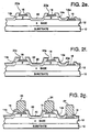
- Figs. 2a-2g a portion of an array, specifically two mesa structures, is shown. It should be realized that a typical array of radiation detectors would comprise a significantly larger number of mesa structures arranged in a linear or a two-dimensional array.
- Processing begins with an n-type radiation absorbing HgCdTe base layer 12 that is grown on an electrically insulating and transparent substrate 10.
- Substrate 10 is selected to be transparent at wavelengths of interest, specifically those wavelengths that are desired to be absorbed within the base layer 12.
- a preferred method for growing the base layer 12 on the substrate 10 is by Liquid Phase Epitaxy (LPE), although Molecular Beam Epitaxy (MBE) and Metal-Organic Chemical Vapor Deposition (MOCVD) are also suitable growth techniques.
- LPE Liquid Phase Epitaxy
- MBE Molecular Beam Epitaxy
- MOCVD Metal-Organic Chemical Vapor Deposition
- a suitable material for the substrate 10 is CdZnTe.
- the bandgap of the HgCdTe semiconductor material of the base layer 12 is selected for absorbing radiation having the wavelengths of interest and is set, in a known fashion, by varying the relative concentrations of the Hg and Cd atoms in accordance with the formula: Hg (1-x) Cd (x) Te, wherein (x) is a nonzero number that is less than one.
- a p-type HgCdTe cap layer 14 may be grown, by example, by LPE, MBE, or by MOCVD.
- a suitable dopant species for the base layer 12 is indium having a concentration of approximately 10 15 atoms/cm 3 .
- a suitable dopant species for the cap layer 14 is arsenic having a concentration of approximately 10 18 atoms/cm 3 .
- Individual photodiodes are delineated by a mesa etch process, using bromine/ethyleneglycol or bromine/methanol, in conjunction with a photolithographically applied mask. The result of the mesa etch is to differentiate the p-type cap layer into a plurality of electrically isolated regions 14a, each of the regions 14a being contained within a mesa and forming a p-n junction with the underlying n-type base layer 12.
- a metal contact pad 16 is also applied to the n-type HgCdTe base layer 12.
- the metal contact pad is comprised of a refractory metal selected to have a low diffusion characteristic, at elevated temperatures, so as to prevent the diffusion of the contact metal into the underlying HgCdTe cap layer 14a.
- a presently preferred metal is Mo.
- a further advantage of Mo is that it exhibits a CTE that is more closely matched to the HgCdTe than is the CTE of many commonly used contact metals, such as Cr and Au.
- a presently preferred technique deposits the Mo contact metalization by sputter deposition and a lift-off process.
- a suitable thickness for the contact pads 16 and 18 is approximately 1.5 x 10 -7 metres (1500 Angstroms).
- a next step overcoats the structure formed thus far with a layer 20 of wide bandgap Group IIB-VIA semiconductor material.
- This wide bandgap semiconductor material may be, by example, CdTe, CdZnTe, or CdSeTe.
- a presently preferred technique is to blanket deposit CdTe to a depth of approximately 4 x 10 -7 metres (4000 Angstroms) by a thermal evaporation process.
- Other suitable deposition techniques include MBE, MOCVD, and sputtering.
- the effect of this step is to cover the exposed surface of the n-type base layer 12, the exposed surfaces of the p-type cap layers 14a, and also the Mo contacts 16 and 18, with a layer or film of the wide bandgap semiconductor material.
- a next step anneals the structure formed thus far in Hg vapor at a first temperature for a first period of time and then at a second, lower temperature for a second period of time.
- both the first and the second temperatures are greater than a temperature used during a subsequent Dewar bake-out process. That is, both the first and the second temperatures are greater than approximately 150°C.
- One result of the anneal is to interchange Hg and Cd at cation sites along an interface between the layers 12 and 14a and the layer 20. This interface region is shown in Fig. 2d in a crosshatched manner.
- windows 20a are opened through the layer 20 to expose the Mo contacts 16 and 18.
- One suitable technique for opening the windows 20a is to employ photoresist patterning in conjunction with a wet chemical etch. Two suitable wet etchants are Br/ethyleneglycol and Br/methanol.
- the windows 20a may also be opened by ion beam milling or by a reactive ion etch process.
- the Mo contacts 16 and 18 beneficially function as etch stops for the etching process.
- the photoresist mask is stripped after opening the windows 20a.
- a dielectric layer 22 comprised of, by example, Si 3 N 4 , SiO 2 , or SiO.
- a suitable method for depositing the dielectric layer 22 is by a plasma process that deposits the layer to a thickness of approximately 1 x 10 -7 metres (1000 Angstroms).
- a photoresist patterning step provides an apertured mask, and windows 22a are opened through the dielectric layer 22 to expose the Mo contacts 16 and 18.
- One suitable technique for opening the windows 22a is to employ photoresist patterning with a wet chemical etch. CF 4 is one suitable wet etchant. The photoresist mask is stripped after opening the windows 22a.
- the structure is photolithographically patterned to provide an indium bump mask, and indium bumps 24 are applied to contact individual ones of the photodiode Mo contact pads 16, and to the common Mo contact pad(s) 18, through the windows 22a.
- One suitable method forms the indium bumps 24 to a thickness of approximately 12 microns through the use of a thermal evaporation technique.
- the In bumps 24 are left exposed, with the underlying Mo contact metallization being buried beneath the dielectric layer 22.
- the dielectric layer 22, or overglass is also substantially impervious to the passage of Hg, and thus beneficially prevents the out-diffusion of Hg from the base layer 12 and the regions 14a.
- the array of PV diodes thus formed is mated to, or hybridized with, a readout circuit through the In bumps 24.
- the In bumps 24 Prior to joining the array to the readout circuit the In bumps 24 are chemically wet etched to remove any surface oxides that would adversely affect the contact resistance.
- An etching procedure such as that described in the aforementioned commonly assigned U.S. Patent No. 4,865,245, issued to E.F. Schulte et al., may be employed.
- the In bumps 24 are exposed to the etchant, the underlying contact metallization being buried beneath the dielectric layer 22.
- the aforementioned problems resulting from the proximity of two dissimilar metals are overcome, the In bumps 24 are uniformly etched over the surface of the array, and In-Te whiskers are not produced.
- the use of the method of the invention thus improves the yield of IR detector arrays by improving the In bump 24 quality during the hybridization process, and also improves reliability by ensuring that the size and shape of the In bumps 24 is maintained at their design dimensions.
- the anneal in Fig. 2d is performed with a CdTe layer 20 that is substantially continuous across the entire surface of the array.
- arrays of PV diodes fabricated in accordance with the invention exhibit stable performance after a 74 hour vacuum bake (Dewar bake-out) at 145°C.
- bake temperatures have been limited to 100°C or less because of the above mentioned instabilities in the surface passivation and/or the diffusion of the contact metal into the HgCdTe.
- both the passivation layer 20 and the Mo contact metal were previously annealed at a substantially higher temperature, neither is expected to change significantly at storage or processing temperatures that are less than the anneal temperature.
- the teaching of the invention is also applicable to n-on-p devices and also to photoconductive, as opposed to photovoltaic, devices.
- the teaching of the invention is also applicable to photoresponsive devices having a planar configuration, wherein a p-n junction is formed within a body of HgCdTe through a diffusion or implantation of an acceptor or a donor species into the body.
Landscapes
- Light Receiving Elements (AREA)
Claims (13)
- Procédé pour fabriquer une diode photovoltaïque, comprenant, dans l'ordre suivant, les étapes dans lesquelles :on réalise une jonction p-n entre une couche (12) de base, développée sur un substrat (10) et constituée d'une matière semiconductrice du groupe IIB-VIA ayant un premier type de conductivité électrique, et une région (14a) de recouvrement constituée d'une matière semiconductrice du groupe IIB-VIA ayant un second type de conductivité électrique ;on forme une électrode (16) de contact métallique sur la région (14a) de recouvrement ;on recouvre la couche (12) de base, la région (14a) de recouvrement et l'électrode (16) de contact métallique pour former une structure revêtue, l'étape de revêtement incluant une étape de dépôt d'une première couche (20) de revêtement constituée d'une matière semiconductrice ayant une bande interdite choisie pour être plus large qu'une bande interdite de la matière semiconductrice de l'une ou l'autre de la couche (12) de base ou de la région (14a) de recouvrement ;on recuit à la chaleur la structure revêtue ;on ouvre une première fenêtre (20a) à travers la première couche revêtue (20) pour exposition, à l'intérieur de la première fenêtre, d'une surface de l'électrode (16) de contact métallique ; eton forme une interconnexion conductrice de l'électricité (24) sur l'électrode (16) de contact métallique pour mise en contact avec un circuit externe, incluant les étapes, dans lesquelles :on recouvre les surfaces exposées de la première couche (20) de revêtement, la première fenêtre (20a) et l'électrode (16) de contact métallique d'une seconde couche (22) de revêtement constituée d'une matière diélectrique ;on ouvre une seconde fenêtre (22a) à travers la seconde couche (22) de recouvrement en alignement avec la première fenêtre (20a) pour exposer, à l'intérieur de la seconde fenêtre (22a), la surface de l'électrode (16) de contact métallique ; eton forme l'interconnexion conductrice de l'électricité (24) à l'intérieur de la seconde fenêtre (22a) et sur la surface exposée de l'électrode (16) de contact métallique de façon que seule une partie de l'interconnexion conductrice de l'électricité (24) soit exposée, et qu'aucune partie de l'électrode (16) de contact métallique sous-jacente ne soit exposée.
- Procédé selon la revendication 1, dans lequel l'étape de réalisation d'une jonction p-n inclut les étapes, dans lesquelles :on réalise la couche (12) de base constituée d'une matière semiconductrice du groupe IIB-VIA ayant un premier type de conductivité électrique, la couche (12) de base comportant une couche de recouvrement sus-jacente constituée d'une matière semiconductrice du groupe IIB-VIA ayant un second type de conductivité électrique ; eton différencie la couche de recouvrement en une pluralité de régions isolées électriquement pour former une pluralité de structures mésa, chacune des structures mésa incluant une interface entre la couche (12) de base et l'une des régions isolées électriquement pour former la jonction p-n.
- Procédé selon la revendication 2, dans lequel ladite couche (12) de base est constituée de HgCdTe de type n, et dans lequel ladite couche de recouvrement est constituée de HgCdTe de type p.
- Procédé selon l'une quelconque des revendications 1 ou 2, dans lequel l'étape de formation d'une électrode (16) de contact métallique sur la région (14a) de recouvrement forme l'électrode (16) de contact métallique avec un métal choisi pour qu'elle ait un coefficient de dilatation thermique qui soit similaire à celui de la région (14a) de recouvrement, le métal étant également choisi pour avoir un faible pouvoir de diffusion dans la région (14a) de recouvrement.
- Procédé selon l'une quelconque des revendications précédentes, dans lequel l'étape de revêtement de la couche (12) de base, de la région (14a) de recouvrement, et de l'électrode (16) de contact métallique inclut une étape de dépôt d'une couche de matière semiconductrice choisie à partir du groupe constitué du CdTe, du CdSeTe, et du CdZnTe.
- Procédé selon l'une quelconque des revendications précédentes, dans lequel l'étape de revêtement de surfaces exposées de la première couche (20) de revêtement, de la première fenêtre (20a) et de l'électrode (16) de contact métallique d'une seconde couche (22) de revêtement constituée de matière diélectrique inclut le dépôt d'une couche de matière choisie à partir du groupe constitué du SiO2, du SiO et du Si3N4.
- Procédé selon l'une quelconque des revendications précédentes, dans lequel l'étape de recuit à la chaleur de la structure revêtue se fait à la vapeur de mercure, et inclut les étapes, dans lesquelles :on utilise une première température pendant une première période de temps ; eton utilise une seconde température plus basse pendant une seconde période de temps.
- Photodiode, comprenant :dans laquelle ladite couche diélectrique (22) est en contact intime avec les surfaces latérales de ladite interconnexion (24) de sorte qu'aucune partie de ladite électrode (16) de contact métallique ne peut être contactée physiquement depuis une surface supérieure de ladite couche diélectrique (22).un substrat (10) ;une région (12) de base semiconductrice recouvrant le substrat (10) et comprenant des éléments choisis à partir du groupe IIB-VIA, ladite région (12) de base ayant un premier type de conductivité électrique ;une région (14a) de recouvrement semiconductrice disposée sur ladite région (12) de base, ladite région (14a) de recouvrement étant constituée d'éléments choisis à partir du groupe IIB-VIA, ladite région (14a) de recouvrement ayant un second type de conductivité électrique et formant une jonction p-n avec ladite région (12) de base ;une électrode (16) de contact métallique conductrice de l'électricité formée sur une surface supérieure de ladite région (14a) de recouvrement ;une couche semiconductrice (20) recouvrant ladite région (12) de base, ladite région (14a) de recouvrement, et recouvrant également partiellement ladite électrode (16) de contact métallique, la couche semiconductrice (20) comprenant des éléments choisis à partir du groupe IIB-VIA, ladite couche semiconductrice (20) ayant une bande interdite plus large qu'une bande interdite de ladite région (12) de base et de ladite région (14a) de recouvrement ;une couche diélectrique (22) recouvrant ladite couche semiconductrice (20) ; etune interconnexion conductrice de l'électricité (24) formée sur ladite électrode (16) de contact métallique, ladite interconnexion (24) s'étendant vers le haut de ladite électrode (16) de contact métallique et à travers ladite couche diélectrique (22) ;
- Photodiode selon la revendication 8, dans laquelle ledit substrat (10) est constitué d'éléments choisis à partir du groupe IIB-VIA.
- Photodiode selon la revendication 8, et comprenant en outre :une seconde électrode (18) de contact métallique conductrice de l'électricité formée sur une surface supérieure de ladite région (12) de base ; etune seconde interconnexion conductrice de l'électricité (24) formée sur ladite seconde électrode (18) de contact métallique, ladite seconde interconnexion (24) s'étendant vers le haut de ladite seconde électrode (18) de contact métallique et à travers ladite couche diélectrique (22), dans laquelle ladite couche diélectrique (22) est en contact intime avec les surfaces latérales de ladite seconde interconnexion (24) de sorte qu'aucune partie de ladite seconde électrode (18) de contact métallique n'est accessible depuis la surface supérieure de ladite couche diélectrique (22).
- Photodiode selon l'une quelconque des revendications 8 à 10, dans laquelle ladite région (12) de base est constituée de HgCdTe de type n, et dans laquelle ladite région (14a) de recouvrement est constituée de HgCdTe de type p.
- Photodiode selon l'une quelconque des revendications 8 à 11, dans laquelle ladite couche semiconductrice (20) est constituée de matière choisie à partir du groupe constitué du CdTe, du CdSeTe, et du CdZnTe.
- Photodiode selon l'une quelconque des revendications 8 à 12, dans laquelle ladite couche diélectrique (22) est constituée de matière choisie à partir du groupe constitué du SiO2, du SiO, et du Si3N4.
Priority Applications (4)
| Application Number | Priority Date | Filing Date | Title |
|---|---|---|---|
| US07/917,562 US5296384A (en) | 1992-07-21 | 1992-07-21 | Bake-stable HgCdTe photodetector and method for fabricating same |
| EP93305794A EP0635892B1 (fr) | 1992-07-21 | 1993-07-22 | Photodétecteur en HgCdTe stable au recuit et procédé pour sa fabrication |
| DE69332060T DE69332060T2 (de) | 1993-07-22 | 1993-07-22 | Glühenbeständiger HgCdTe-Photodetektor und Herstellungsverfahren |
| US08/270,527 US5401986A (en) | 1992-07-21 | 1994-07-05 | Bake-stable HgCdTe photodetector with II-VI passivation layer |
Applications Claiming Priority (3)
| Application Number | Priority Date | Filing Date | Title |
|---|---|---|---|
| US07/917,562 US5296384A (en) | 1992-07-21 | 1992-07-21 | Bake-stable HgCdTe photodetector and method for fabricating same |
| EP93305794A EP0635892B1 (fr) | 1992-07-21 | 1993-07-22 | Photodétecteur en HgCdTe stable au recuit et procédé pour sa fabrication |
| US08/270,527 US5401986A (en) | 1992-07-21 | 1994-07-05 | Bake-stable HgCdTe photodetector with II-VI passivation layer |
Publications (2)
| Publication Number | Publication Date |
|---|---|
| EP0635892A1 EP0635892A1 (fr) | 1995-01-25 |
| EP0635892B1 true EP0635892B1 (fr) | 2002-06-26 |
Family
ID=27235453
Family Applications (1)
| Application Number | Title | Priority Date | Filing Date |
|---|---|---|---|
| EP93305794A Expired - Lifetime EP0635892B1 (fr) | 1992-07-21 | 1993-07-22 | Photodétecteur en HgCdTe stable au recuit et procédé pour sa fabrication |
Country Status (2)
| Country | Link |
|---|---|
| US (1) | US5401986A (fr) |
| EP (1) | EP0635892B1 (fr) |
Cited By (3)
| Publication number | Priority date | Publication date | Assignee | Title |
|---|---|---|---|---|
| US11851785B2 (en) | 2021-05-21 | 2023-12-26 | Raytheon Company | Aluminum nitride passivation layer for mercury cadmium telluride in an electrical device |
| US11894477B2 (en) | 2021-05-17 | 2024-02-06 | Raytheon Company | Electrical device with stress buffer layer and stress compensation layer |
| US12002773B2 (en) | 2021-03-03 | 2024-06-04 | Raytheon Company | Hybrid pocket post and tailored via dielectric for 3D-integrated electrical device |
Families Citing this family (22)
| Publication number | Priority date | Publication date | Assignee | Title |
|---|---|---|---|---|
| GB2289983B (en) | 1994-06-01 | 1996-10-16 | Simage Oy | Imaging devices,systems and methods |
| US5942788A (en) * | 1995-05-09 | 1999-08-24 | Minolta Co., Ltd. | Solid state image sensing device |
| US5846850A (en) * | 1995-09-05 | 1998-12-08 | Raytheon Ti Systems, Inc. | Double sided interdiffusion process and structure for a double layer heterojunction focal plane array |
| US5646426A (en) * | 1995-12-12 | 1997-07-08 | Santa Barbara Research Center | Contact metal diffusion barrier for semiconductor devices |
| US5998235A (en) | 1997-06-26 | 1999-12-07 | Lockheed Martin Corporation | Method of fabrication for mercury-based quaternary alloys of infrared sensitive materials |
| RU2131632C1 (ru) * | 1997-07-14 | 1999-06-10 | Институт физики полупроводников СО РАН | Способ сборки фотоприемных устройств |
| US9029793B2 (en) | 1998-11-05 | 2015-05-12 | Siemens Aktiengesellschaft | Imaging device |
| DE10037103A1 (de) * | 2000-07-27 | 2002-02-14 | Aeg Infrarot Module Gmbh | Multispektrale Photodiode |
| JP4208172B2 (ja) * | 2000-10-31 | 2009-01-14 | シャープ株式会社 | フォトダイオードおよびそれを用いた回路内蔵受光素子 |
| US6803322B1 (en) * | 2000-12-15 | 2004-10-12 | Science Applications International Corporation | Pin alloy-semiconductor, radiation detectors with rectifying junction contacts, methods and systems for forming pin alloy-semiconductor devices with rectifying junction contacts, and systems and methods for analyzing alloy-semiconductor properties |
| GB0224689D0 (en) | 2002-10-23 | 2002-12-04 | Simage Oy | Formation of contacts on semiconductor substrates |
| JP2006504258A (ja) | 2002-10-25 | 2006-02-02 | ゴールドパワー リミテッド | 回路基板およびその製造方法 |
| FR2869462B1 (fr) * | 2004-04-21 | 2006-06-02 | Fr De Detecteurs Infrarouges S | Procede pour la realisation d'un detecteur de rayonnement electromagnetique, et notamment infrarouge |
| KR100723457B1 (ko) * | 2006-09-20 | 2007-05-31 | (주)한비젼 | 반도체 소자 |
| US7544532B2 (en) * | 2006-10-17 | 2009-06-09 | Raytheon Company | Infrared photodiodes and sensor arrays with improved passivation layers and methods of manufacture |
| CN100541146C (zh) * | 2007-04-25 | 2009-09-16 | 中国科学院上海技术物理研究所 | 防非红外辐射入射面响应的碲镉汞红外探测器芯片 |
| RU2392691C1 (ru) * | 2009-03-16 | 2010-06-20 | Федеральное государственное унитарное предприятие "НПО "ОРИОН" | Фотоприемное устройство |
| DE102013214575B3 (de) * | 2013-07-25 | 2014-09-18 | Siemens Aktiengesellschaft | Halbleiterelement mit Lötstopplage und Verfahren zu seiner Erzeugung sowie Strahlungsdetektor und medizintechnisches Gerät mit einem solchen Strahlungsdetektor |
| US11121302B2 (en) | 2018-10-11 | 2021-09-14 | SeeQC, Inc. | System and method for superconducting multi-chip module |
| CN110416324A (zh) * | 2019-08-22 | 2019-11-05 | 浙江正泰太阳能科技有限公司 | 一种太阳能电池及其制备方法 |
| IL297009B2 (en) * | 2020-04-09 | 2025-11-01 | Commissariat Energie Atomique | Process for manufacturing a low-noise photodetector device in a cdhgte substrate |
| US20220416095A1 (en) * | 2021-06-29 | 2022-12-29 | Raytheon Company | Low-stress dielectric layer, planarization method, and low-temperature processing for 3d-integrated electrical device |
Family Cites Families (28)
| Publication number | Priority date | Publication date | Assignee | Title |
|---|---|---|---|---|
| FR2168934B1 (fr) * | 1972-01-27 | 1977-04-01 | Telecommunications Sa | |
| FR2281650A1 (fr) * | 1974-08-06 | 1976-03-05 | Telecommunications Sa | Procede de fabrication d'une photodiode sensible aux rayonnements infrarouges et photodiode obtenue par ce procede |
| US4000508A (en) * | 1975-07-17 | 1976-12-28 | Honeywell Inc. | Ohmic contacts to p-type mercury cadmium telluride |
| FR2336804A1 (fr) * | 1975-12-23 | 1977-07-22 | Telecommunications Sa | Perfectionnements apportes aux dispositifs semi-conducteurs, notamment aux detecteurs photovoltaiques comprenant un substrat a base d'un alliage cdxhg1-xte, et procede de fabrication d'un tel dispositif perfectionne |
| US4206003A (en) * | 1977-07-05 | 1980-06-03 | Honeywell Inc. | Method of forming a mercury cadmium telluride photodiode |
| DE2739309A1 (de) * | 1977-09-01 | 1979-03-15 | Licentia Gmbh | Infrarot-detektorzelle |
| USRE30412E (en) * | 1979-04-26 | 1980-10-07 | Eastman Kodak Company | CdTe Barrier type photovoltaic cells with enhanced open-circuit voltage, and process of manufacture |
| FR2488048A1 (fr) * | 1980-07-30 | 1982-02-05 | Telecommunications Sa | Detecteur photovoltaique sensible dans l'infrarouge proche |
| EP0068652B1 (fr) * | 1981-06-24 | 1988-05-25 | The Secretary of State for Defence in Her Britannic Majesty's Government of the United Kingdom of Great Britain and | Photodiodes |
| US4439912A (en) * | 1982-04-19 | 1984-04-03 | The United States Of America As Represented By The Secretary Of The Army | Infrared detector and method of making same |
| US4549195A (en) * | 1983-04-14 | 1985-10-22 | Westinghouse Electric Corp. | Heterojunction semiconductor device |
| JPS603165A (ja) * | 1983-06-20 | 1985-01-09 | Matsushita Electric Ind Co Ltd | 受光素子 |
| US4611091A (en) * | 1984-12-06 | 1986-09-09 | Atlantic Richfield Company | CuInSe2 thin film solar cell with thin CdS and transparent window layer |
| US4639756A (en) * | 1986-05-05 | 1987-01-27 | Santa Barbara Research Center | Graded gap inversion layer photodiode array |
| FR2604298B1 (fr) * | 1986-09-19 | 1988-10-28 | Commissariat Energie Atomique | Procede de realisation d'une prise de contact electrique sur un substrat en hgcdte de conductivite p et application a la fabrication d'une diode n/p |
| US4764261A (en) * | 1986-10-31 | 1988-08-16 | Stemcor Corporation | Method of making improved photovoltaic heterojunction structures |
| US4735662A (en) * | 1987-01-06 | 1988-04-05 | The Standard Oil Company | Stable ohmic contacts to thin films of p-type tellurium-containing II-VI semiconductors |
| US4865245A (en) * | 1987-09-24 | 1989-09-12 | Santa Barbara Research Center | Oxide removal from metallic contact bumps formed on semiconductor devices to improve hybridization cold-welds |
| US4818565A (en) * | 1987-10-30 | 1989-04-04 | Regents Of The University Of Minnesota | Method to stabilize metal contacts on mercury-cadmium-telluride alloys |
| JPH01223779A (ja) * | 1988-03-03 | 1989-09-06 | Toshiba Corp | 赤外線検出器 |
| JP2670289B2 (ja) * | 1988-03-31 | 1997-10-29 | 株式会社東芝 | 赤外線検出用フオトダイオードおよびその製造方法 |
| US5189297A (en) * | 1988-08-29 | 1993-02-23 | Santa Barbara Research Center | Planar double-layer heterojunction HgCdTe photodiodes and methods for fabricating same |
| US5144138A (en) * | 1989-10-06 | 1992-09-01 | Texas Instruments Incorporated | Infrared detector and method |
| JPH03196683A (ja) * | 1989-12-26 | 1991-08-28 | Nec Corp | テルル化水銀カドミウム赤外線検出器 |
| US5149956A (en) * | 1991-06-12 | 1992-09-22 | Santa Barbara Research Center | Two-color radiation detector array and methods of fabricating same |
| US5192695A (en) * | 1991-07-09 | 1993-03-09 | Fermionics Corporation | Method of making an infrared detector |
| JP2809908B2 (ja) * | 1991-09-30 | 1998-10-15 | 三菱電機株式会社 | 固体撮像素子 |
| US5279974A (en) * | 1992-07-24 | 1994-01-18 | Santa Barbara Research Center | Planar PV HgCdTe DLHJ fabricated by selective cap layer growth |
-
1993
- 1993-07-22 EP EP93305794A patent/EP0635892B1/fr not_active Expired - Lifetime
-
1994
- 1994-07-05 US US08/270,527 patent/US5401986A/en not_active Expired - Lifetime
Cited By (3)
| Publication number | Priority date | Publication date | Assignee | Title |
|---|---|---|---|---|
| US12002773B2 (en) | 2021-03-03 | 2024-06-04 | Raytheon Company | Hybrid pocket post and tailored via dielectric for 3D-integrated electrical device |
| US11894477B2 (en) | 2021-05-17 | 2024-02-06 | Raytheon Company | Electrical device with stress buffer layer and stress compensation layer |
| US11851785B2 (en) | 2021-05-21 | 2023-12-26 | Raytheon Company | Aluminum nitride passivation layer for mercury cadmium telluride in an electrical device |
Also Published As
| Publication number | Publication date |
|---|---|
| EP0635892A1 (fr) | 1995-01-25 |
| US5401986A (en) | 1995-03-28 |
Similar Documents
| Publication | Publication Date | Title |
|---|---|---|
| EP0635892B1 (fr) | Photodétecteur en HgCdTe stable au recuit et procédé pour sa fabrication | |
| US4070689A (en) | Semiconductor solar energy device | |
| US6657194B2 (en) | Multispectral monolithic infrared focal plane array detectors | |
| US4972244A (en) | Photodiode and photodiode array on a II-VI material and processes for the production thereof | |
| US3508126A (en) | Semiconductor photodiode with p-n junction spaced from heterojunction | |
| US5185648A (en) | Plural-wavelength infrared detector devices | |
| US4665609A (en) | Process of manufacturing a photosensitive device having a plurality of detectors separated by zones impervious to the radiation to be detected | |
| US4949144A (en) | Semiconductor photo-detector having a two-stepped impurity profile | |
| US4897123A (en) | Solar cells and method for producing solar cells | |
| US5189297A (en) | Planar double-layer heterojunction HgCdTe photodiodes and methods for fabricating same | |
| US4794439A (en) | Rear entry photodiode with three contacts | |
| EP0068652B1 (fr) | Photodiodes | |
| US5279974A (en) | Planar PV HgCdTe DLHJ fabricated by selective cap layer growth | |
| US20030102432A1 (en) | Monolithic infrared focal plane array detectors | |
| US5608255A (en) | FET optical receiver using backside illumination, indium materials species | |
| US5296384A (en) | Bake-stable HgCdTe photodetector and method for fabricating same | |
| US4956304A (en) | Buried junction infrared photodetector process | |
| US5646426A (en) | Contact metal diffusion barrier for semiconductor devices | |
| US5599733A (en) | Method using cadmium-rich CdTe for lowering the metal vacancy concentrations of HgCdTe surfaces | |
| US4875082A (en) | Schottky barrier photodiode structure | |
| US4742017A (en) | Implantation method for forming Schottky barrier photodiodes | |
| KR100422294B1 (ko) | Cd/Hg 분위기에서 열처리에 의한 HgCdTe 접합다이오드의 패시배이션 방법 | |
| US6198100B1 (en) | Method for fabricating an infrared radiation detector | |
| US5187378A (en) | Photodetector | |
| IL106458A (en) | Bake-stable HgCdTe photodetector and method for fabricating same |
Legal Events
| Date | Code | Title | Description |
|---|---|---|---|
| PUAI | Public reference made under article 153(3) epc to a published international application that has entered the european phase |
Free format text: ORIGINAL CODE: 0009012 |
|
| AK | Designated contracting states |
Kind code of ref document: A1 Designated state(s): DE ES FR GB IT NL |
|
| 17P | Request for examination filed |
Effective date: 19950630 |
|
| 17Q | First examination report despatched |
Effective date: 19971031 |
|
| RAP1 | Party data changed (applicant data changed or rights of an application transferred) |
Owner name: RAYTHEON COMPANY |
|
| GRAG | Despatch of communication of intention to grant |
Free format text: ORIGINAL CODE: EPIDOS AGRA |
|
| GRAG | Despatch of communication of intention to grant |
Free format text: ORIGINAL CODE: EPIDOS AGRA |
|
| GRAH | Despatch of communication of intention to grant a patent |
Free format text: ORIGINAL CODE: EPIDOS IGRA |
|
| GRAH | Despatch of communication of intention to grant a patent |
Free format text: ORIGINAL CODE: EPIDOS IGRA |
|
| GRAA | (expected) grant |
Free format text: ORIGINAL CODE: 0009210 |
|
| AK | Designated contracting states |
Kind code of ref document: B1 Designated state(s): DE ES FR GB IT NL |
|
| PG25 | Lapsed in a contracting state [announced via postgrant information from national office to epo] |
Ref country code: NL Free format text: LAPSE BECAUSE OF FAILURE TO SUBMIT A TRANSLATION OF THE DESCRIPTION OR TO PAY THE FEE WITHIN THE PRESCRIBED TIME-LIMIT Effective date: 20020626 |
|
| REG | Reference to a national code |
Ref country code: GB Ref legal event code: FG4D |
|
| REF | Corresponds to: |
Ref document number: 69332060 Country of ref document: DE Date of ref document: 20020801 |
|
| ET | Fr: translation filed | ||
| NLV1 | Nl: lapsed or annulled due to failure to fulfill the requirements of art. 29p and 29m of the patents act | ||
| PG25 | Lapsed in a contracting state [announced via postgrant information from national office to epo] |
Ref country code: ES Free format text: LAPSE BECAUSE OF FAILURE TO SUBMIT A TRANSLATION OF THE DESCRIPTION OR TO PAY THE FEE WITHIN THE PRESCRIBED TIME-LIMIT Effective date: 20021220 |
|
| PLBE | No opposition filed within time limit |
Free format text: ORIGINAL CODE: 0009261 |
|
| STAA | Information on the status of an ep patent application or granted ep patent |
Free format text: STATUS: NO OPPOSITION FILED WITHIN TIME LIMIT |
|
| 26N | No opposition filed |
Effective date: 20030327 |
|
| PGFP | Annual fee paid to national office [announced via postgrant information from national office to epo] |
Ref country code: GB Payment date: 20050615 Year of fee payment: 13 |
|
| PGFP | Annual fee paid to national office [announced via postgrant information from national office to epo] |
Ref country code: DE Payment date: 20050617 Year of fee payment: 13 |
|
| PG25 | Lapsed in a contracting state [announced via postgrant information from national office to epo] |
Ref country code: GB Free format text: LAPSE BECAUSE OF NON-PAYMENT OF DUE FEES Effective date: 20060722 |
|
| PGFP | Annual fee paid to national office [announced via postgrant information from national office to epo] |
Ref country code: IT Payment date: 20060731 Year of fee payment: 14 |
|
| PG25 | Lapsed in a contracting state [announced via postgrant information from national office to epo] |
Ref country code: DE Free format text: LAPSE BECAUSE OF NON-PAYMENT OF DUE FEES Effective date: 20070201 |
|
| GBPC | Gb: european patent ceased through non-payment of renewal fee |
Effective date: 20060722 |
|
| PG25 | Lapsed in a contracting state [announced via postgrant information from national office to epo] |
Ref country code: IT Free format text: LAPSE BECAUSE OF NON-PAYMENT OF DUE FEES Effective date: 20070722 |
|
| PGFP | Annual fee paid to national office [announced via postgrant information from national office to epo] |
Ref country code: FR Payment date: 20120719 Year of fee payment: 20 |