EP0635911A2 - Elektrischer Verbinder mit Flachen, elastischen Mehrfachkontaktelementen - Google Patents
Elektrischer Verbinder mit Flachen, elastischen Mehrfachkontaktelementen Download PDFInfo
- Publication number
- EP0635911A2 EP0635911A2 EP94111490A EP94111490A EP0635911A2 EP 0635911 A2 EP0635911 A2 EP 0635911A2 EP 94111490 A EP94111490 A EP 94111490A EP 94111490 A EP94111490 A EP 94111490A EP 0635911 A2 EP0635911 A2 EP 0635911A2
- Authority
- EP
- European Patent Office
- Prior art keywords
- contact
- holes
- opposite
- extending
- connection objects
- Prior art date
- Legal status (The legal status is an assumption and is not a legal conclusion. Google has not performed a legal analysis and makes no representation as to the accuracy of the status listed.)
- Granted
Links
Images


Classifications
-
- H—ELECTRICITY
- H01—ELECTRIC ELEMENTS
- H01R—ELECTRICALLY-CONDUCTIVE CONNECTIONS; STRUCTURAL ASSOCIATIONS OF A PLURALITY OF MUTUALLY-INSULATED ELECTRICAL CONNECTING ELEMENTS; COUPLING DEVICES; CURRENT COLLECTORS
- H01R12/00—Structural associations of a plurality of mutually-insulated electrical connecting elements, specially adapted for printed circuits, e.g. printed circuit boards [PCB], flat or ribbon cables, or like generally planar structures, e.g. terminal strips, terminal blocks; Coupling devices specially adapted for printed circuits, flat or ribbon cables, or like generally planar structures; Terminals specially adapted for contact with, or insertion into, printed circuits, flat or ribbon cables, or like generally planar structures
- H01R12/70—Coupling devices
- H01R12/82—Coupling devices connected with low or zero insertion force
- H01R12/85—Coupling devices connected with low or zero insertion force contact pressure producing means, contacts activated after insertion of printed circuits or like structures
- H01R12/89—Coupling devices connected with low or zero insertion force contact pressure producing means, contacts activated after insertion of printed circuits or like structures acting manually by moving connector housing parts linearly, e.g. slider
-
- H—ELECTRICITY
- H01—ELECTRIC ELEMENTS
- H01R—ELECTRICALLY-CONDUCTIVE CONNECTIONS; STRUCTURAL ASSOCIATIONS OF A PLURALITY OF MUTUALLY-INSULATED ELECTRICAL CONNECTING ELEMENTS; COUPLING DEVICES; CURRENT COLLECTORS
- H01R13/00—Details of coupling devices of the kinds covered by groups H01R12/70 or H01R24/00 - H01R33/00
- H01R13/02—Contact members
- H01R13/193—Means for increasing contact pressure at the end of engagement of coupling part, e.g. zero insertion force or no friction
Definitions
- This invention relates to a connector for use in electrically connecting a pair of connection objects opposite to each other in a first direction and, in particular, to a connector which can carry out connection and disconnection between the connection objects in accordance with a relative movement of the connection objects in a second direction perpendicular to the first direction.
- JP(Y2) 1-42309) a conventional connector of the type is disclosed in Japanese Utility Model Publication No. 42309/1989 (JP(Y2) 1-42309).
- the connector is for electrically connecting two pin contacts to each other and includes an electroconductive socket contact.
- the socket contact has two socket portions each having a size that allows the pin contact to be loosely fitted or inserted thereinto, and a flexible elastic portion connecting these socket portions to each other.
- the pin contacts Prior to electrical connection, the pin contacts are inserted into the respective socket portions. In this event, no special force is required for insertion of the contacts since each socket portion has such the size to allow the pin contact to be loosely inserted thereinto. Accordingly, the conventional connector will be called a zero-insertion force connector.
- the above-mentioned connector uses the socket contact including two socket portions formed at opposite ends of the flexible elastic portion and, therefore, has a complicated structure.
- the use of socket contacts makes it difficult to assemble a high-density small-sized connector and reduces the productivity thereof.
- a positioning member may be necessary to hold the socket portions at preselected positions. It is generally difficult to install the positioning member because of complicated structure of the socket portions. This will readily be understood in view of the fact that the connector disclosed in the above-mentioned publication comprises no positioning member. Accordingly, the socket portions may suffer from misalignment. In this event, the pin contacts fail to be correctly inserted into the socket portions.
- the present invention can be applied to an electrical connector for use in electrically connecting a pair of connection objects to each other, the connection objects being opposite to each other in a first direction and having a relative position changeable between a first and a second position in a second direction perpendicular to the first direction, each of the connection objects having a plurality of holes formed therein each extending in the first direction and having electroconductive contact means therein, the plurality of holes being arranged in a third direction perpendicular to the first direction and the second direction to form a row of holes.
- the connector comprises a flat and elastic multi-contact member comprising a flat insulator sheet generally extending in the first direction and a plurality of parallel conductive strips formed on the flat insulator sheet and extending in parallel with each other in the first direction, the multi-contact member having opposite end portions, each of the end portions being separated into a plurality of tab portions spaced from each other in the third direction and corresponding to the plurality of conductive strips, the a plurality of tabs being loosely fitted into the plurality of holes, respectively, in each of the connection objects when the relative position is the first position, each of the tabs being brought into press contact with the contact means in the corresponding one of the holes at two different points which are on opposite surfaces and spaced from each other in the first direction while the multi-contact member being elastically bent when the relative position is the second position.
- each of the contact means in each of the holes is separated in the second direction into two contact pieces.
- the multi-contact member further comprises a second conductive layer formed on an opposite surface of the flat insulator sheet.
- the second conductive layer is separated in the second direction into a plurality of conductive strips in registry with the first conductive strips.
- the second conductive layer may be formed to overlie the entire surface of the opposite surface.
- the electric connector further comprises a pair of insulator housings opposite to each other in the first direction and relatively movable in the second direction, each of the housings having a positioning slot for receiving each one of generally half portions of the multi-contact member in the first direction.
- a preferred embodiment of the present invention is directed to an electric connector for use in electrically connecting a pair of connection objects to each other, the connection objects being opposite to each other in a first direction and having a relative position changeable between a first and a second position in a second direction perpendicular to the first direction, each of the connection objects having a plurality of holes formed therein each extending in the first direction and having electroconductive contact means therein, the plurality of holes being arranged in columns and row of a matrix pattern, each of columns extending the second direction and each of rows extending a third direction perpendicular to the first direction and the second direction.
- the connector comprising a plurality of flat and elastic multi-contact members disposed with spaces left between adjacent ones in the second direction and being corresponding to those between adjacent rows, each of the multi-contact members being disposed in a plane extending in the first direction and the third direction, each of the multi-contact members comprising a flat insulator sheet generally extending in the first direction and a plurality of parallel conductive strips formed on the flat insulator sheet and extending in parallel with each other in the first direction, each of the multi-contact member having opposite end portions, each of the end portions being separated into a plurality of tab portions spaced from each other in the third direction and corresponding to the plurality of conductive strips, the a plurality of tab portions of each of the multi-contact members being loosely fitted into the plurality of holes in the corresponding one of the rows, respectively, in each of the connection objects when the relative position is the first position, each of the tab portions being brought into press contact with the contact means in the corresponding one of the holes at two different points which are on opposite surfaces and spaced from each other
- the conductive layer on the multi-contact member is made of conductive and elastic material such as phosphorus bronze, beryllium copper, and stainless steel, so that the multi-contact member is insured to have the elasticity.
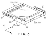
- an electrical connector 11 is for use in electrically connecting a pair of connection objects 12a and 12b (see Fig. 1) to each other.
- the connection objects 12a and 12b are, for example, printed boards, LSI, and others.
- connection objects 12a and 12b are opposite to each other in a first direction (Y direction) and have a relative position changeable between a first and a second position in a second direction (X direction) perpendicular to the first direction Y.
- Y direction first direction
- X direction second direction
- the relative position of the connection objects 12a and 12b is the second position.
- connection objects 12a and 12b has a plurality of holes 13 formed to extend in the first direction Y therein. Holes 13 in connection objects 12a and 12b are denoted with suffixes "a" and “b” as 13a and 13b, respectively.
- Each of the holes has electroconductive contact means which may be made of an electroconductive film coated on the inner surface of the hole, a socket contact fitted thereinto.
- each of the contact means comprises two contact pieces separated in the second direction X, that is, the two contact pieces are shown as two pin contacts 14 and 15 of a plate type or a rod type fitted in each of the holes, which are shown with suffixes "a” and "b” for connection objects 12a and 12b.
- connection objects 12a and 12b the plurality of holes 13a and 13b are arranged in columns and rows of a matrix pattern. Each of columns extends in the second direction X and each of rows extends in a third direction Z perpendicular to the first direction Y and the second direction X.
- the connector 11 comprises a plurality of flat and elastic multi-contact members 16 disposed with spaces left between adjacent ones in the second direction X. The spaces are corresponding to those between adjacent rows of the holes 13.
- Each of the multi-contact members 16 is disposed in a plane extending in the first direction Y and the third direction Z.
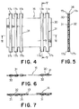
- Each of the multi-contact members 16 has opposite end portions in the first direction Y and each of the end portions is separated into a plurality of tab portions 17a and 17b spaced from each other in the third direction Z. Separation of tab portions 17a are clearly shown in Fig. 2.
- the tab portions 17a and 17b are loosely fitted into holes 13a and 13b in the connection objects 12a and 12b, respectively.
- the multi-contact member 16 will later be described in detail in connection with Figs. 4-7.
- the connector 11 further comprises a pair of insulator housings 18a and 18b opposite to each other in the first direction Y and relatively movable in the second direction X.
- each of housings 18a and 18b is a generally rectangle plate and has an guide grooves 19 in upstanding walls 20 from its upper surface at half portions of opposite sides thereof. Ribs 21 are formed at other half portions at opposite side surfaces of each of the housings 18a and 18b. Two housings 18a and 18b are superposed in a reverse symmetrical condition and are combined with each other to be telescopically moved in the second direction X. In detail, the ribs 21 of each one of housings 18a and 18b are slidably fitted into guide grooves 19 in the other one of the housings 18a and 18b so that the two housings 18a and 18b are relatively movable in the second direction X.
- each of the housings 18a and 18b has a plurality of positioning slots 22a and 22b extending in the third direction Z and along rows of holes 13, respectively.
- Each of the positioning slots is for receiving each one of half portions of the multi-contact members 16 in the first direction Y.
- each of housings 18a and 18b is provided with a plurality of projections 23a and 23b upstanding on one surface thereof. That is, the upper housing 12a in the first direction Y has four projections 23a at four corners on the top surface, while the lower housing 18b also has four projections 23b on the bottom surface thereof.
- the connection objects 12a and 12b are provided with engagement holes 24a and 24b for engaging projections 23a and 23b, respectively. As a result, the housings 18a and 18b can be moved together with the connection objects 12a and 12b, respectively, in the first direction X.
- connection objects 12a and 12b are positioned at the second relative position in the second direction X.
- opposite ends 25a of the housing 18a are offset from the opposite ends 25b of the other housing 18b in the second direction X by a predetermined distance.
- opposite ends 25a of the hosing 18a are in registry with the opposite ends 25b of the other housing 18b, as shown in Fig. 2 and as shown in Fig. 1 by an imaginary line 25'b.
- holes 13b of the lower connection object 12b in Fig.
- each of the multi-contact members 16 is in a plane extending in the first direction Y and the third direction Z.
- each of the multi-contact members 16 comprises a flat flexible insulator sheet 30 generally extending in the first direction Y and a plurality of parallel conductive strips 31 formed on one surface of the flat insulator sheet 30 and extending in parallel with each other in the first direction Y.
- the strips 31 are spaced between adjacent ones by a space equal to that between adjacent ones of the holes 13 arranged in each of the columns.
- each of the multi-contact members 16 has opposite end portions in the first direction Y. Each of the end portions is separated into a plurality of tab portions 17a and 17b in the third direction Z.
- the tab portions 17a and 17b are corresponding to the conductive strips 31.
- the multi-contact member 16 in addition to the conductive strips 31 as a first conductive layer, the multi-contact member 16 further comprises a second conductive layer 32 formed on an opposite surface of the flat insulator sheet 30, as shown in Fig. 5.
- the second conductive layer 32 is a plurality of conductive strips separated in the second direction and in registry with the first conductive strips 31, as shown in Fig. 6.
- the second conductive layer 32 may be formed as an integral body to overlie the entire surface of the opposite surface, as shown in Fig. 7.
- the conductive layers such as strips 31 and 32 is made of conductive and elastic material, for example, phosphorus bronze, beryllium copper, stainless steel, and others.
- the multi-contact member has elasticity.
- a plurality of the multi-contact members 16 are inserted into positioning slots 22a and 22b of the housings 18a and 18b superposed together and tab portions 17a and 17b at opposite end portions project out of the housings 18a and 18b, respectively, as shown in Figs. 1 and 8. It is shown in Fig. 2 that the tab portions 17a project from the upper housing 18a and arranged in columns and rows of a matrix.
- each of slots 22a and 22b is a groove having a bottom wall.
- the bottom wall has a plurality of holes through which tabs 17a and 17b are projected from each of the housings 18a and 18b.
- connection objects 12a and 12b when the connection objects 12a and 12b are positioned at the first relative position so that the housings 18a and 18b are also positioned at the first relative position as shown by the imaginary lines 25'b, the holes 13a and 13b and slots 22a and 22b are linearly arranged in the first direction Y so that each of the multi-contact members 16 is in a plane extending in the first direction Y and the third direction Z, as described above. Accordingly, the tab portions 17a and 17b of each of the multi-contact members 16 are loosely inserted or fitted into the plurality of holes 13a and 13b in the corresponding one of the rows, respectively, in each of the connection objects 12a and 12b.
- each of the multi-contact members 16 is elastically bent and each of the tab portions 17a and 17b is brought into press contact with the pin contacts 14 and 15 in the corresponding one of the holes 13 at two different points, as shown at 33 and 34 for one tab portions at the upper center in the figure, which are on opposite surfaces and spaced from each other in the first direction Y.
- each of the conductive strips 31 on one surface of each multi-contact members 16 is insured to come contact with pin contacts 14a and 14b in the corresponding holes 13a and 13b in the connection objects 12a and 12b, so that the contacts 14a and 14b are electrically connected through the conductive strip 31
- pin contacts 15a and 15b in the corresponding holes 13a and 13b of the connection objects 12a and 12b are electrically connected to each other through each of conductive strips 32 on the opposite surface of each multi-contact member 16.
- independent electrical connection can be realized at opposite surfaces of the thin multi-contact member 16. This means reduction of size of the connector with a high contact density.
- contacts 14 and 15 in one hole 13 can be connected together to form one contact part to which the opposite conductive strips 31 and 32 are commonly connected.
- the multi-contact member 16 can be made to have conductive strips 31 on only one surface. In the case, it is natural that a single contact may be disposed in each of the holes 13.
- contacts 15 in holes 13 in one row are commonly connected and can be used as the ground to improve the high frequency properties.
Landscapes
- Coupling Device And Connection With Printed Circuit (AREA)
Applications Claiming Priority (2)
| Application Number | Priority Date | Filing Date | Title |
|---|---|---|---|
| JP40442/93 | 1993-07-23 | ||
| JP1993040442U JP2547893Y2 (ja) | 1993-07-23 | 1993-07-23 | コネクタ |
Publications (3)
| Publication Number | Publication Date |
|---|---|
| EP0635911A2 true EP0635911A2 (de) | 1995-01-25 |
| EP0635911A3 EP0635911A3 (de) | 1996-06-12 |
| EP0635911B1 EP0635911B1 (de) | 1999-03-24 |
Family
ID=12580767
Family Applications (1)
| Application Number | Title | Priority Date | Filing Date |
|---|---|---|---|
| EP94111490A Expired - Lifetime EP0635911B1 (de) | 1993-07-23 | 1994-07-22 | Elektrischer Verbinder mit Flachen, elastischen Mehrfachkontaktelementen |
Country Status (4)
| Country | Link |
|---|---|
| US (1) | US5470245A (de) |
| EP (1) | EP0635911B1 (de) |
| JP (1) | JP2547893Y2 (de) |
| DE (1) | DE69417311T2 (de) |
Cited By (1)
| Publication number | Priority date | Publication date | Assignee | Title |
|---|---|---|---|---|
| EP0684663A3 (de) * | 1994-05-25 | 1997-04-09 | Japan Aviation Electron | Steckverbinder verwendbar mit relativ geringer operativer Kraft. |
Families Citing this family (8)
| Publication number | Priority date | Publication date | Assignee | Title |
|---|---|---|---|---|
| JPS58146691A (ja) * | 1982-02-26 | 1983-09-01 | 木村 榮治 | 脚立装置 |
| JP2678886B2 (ja) * | 1994-10-06 | 1997-11-19 | 日本航空電子工業株式会社 | 板状回路体用無挿抜力コネクタ |
| JP5092243B2 (ja) | 2006-02-02 | 2012-12-05 | 船井電機株式会社 | 狭ピッチフレキシブル配線 |
| JP5334997B2 (ja) * | 2008-01-17 | 2013-11-06 | アンフェノル・コーポレーション | インターポーザ・アセンブリ及び方法 |
| US7753695B2 (en) * | 2008-04-02 | 2010-07-13 | Hon Hai Precision Ind. Co., Ltd. | Socket with wire-shaped contacts |
| US8979562B2 (en) | 2012-07-25 | 2015-03-17 | Fci Americas Technology Llc | Bus bar lockingly attached to a housing of an electrical connector and its end inserted between rows of power contacts of the electrical connector |
| CN109088290B (zh) * | 2018-08-21 | 2025-03-21 | 博洛尼智能科技(青岛)有限公司 | 活动导电装置及板式结构的家具 |
| JP7181769B2 (ja) * | 2018-11-14 | 2022-12-01 | モレックス エルエルシー | コネクタ |
Family Cites Families (10)
| Publication number | Priority date | Publication date | Assignee | Title |
|---|---|---|---|---|
| US4540229A (en) * | 1982-04-12 | 1985-09-10 | At&T Bell Laboratories | Electrical interconnection apparatus |
| JPS61118979A (ja) * | 1984-11-15 | 1986-06-06 | 第一電子工業株式会社 | 多極接触子 |
| JPS6442309A (en) * | 1987-08-05 | 1989-02-14 | Idemitsu Kosan Co | Method for recovering sulfur |
| JPH0338782Y2 (de) * | 1988-02-03 | 1991-08-15 | ||
| DE3909284A1 (de) * | 1989-03-21 | 1990-09-27 | Nixdorf Computer Ag | Steckkontaktanordnung |
| US5037311A (en) * | 1989-05-05 | 1991-08-06 | International Business Machines Corporation | High density interconnect strip |
| JPH03222276A (ja) * | 1990-01-26 | 1991-10-01 | Dai Ichi Denshi Kogyo Kk | 非接着部を備えた多層電気接触子形成材の製造方法 |
| JPH0521119A (ja) * | 1991-07-02 | 1993-01-29 | Augat Inc | 多極コネクタ |
| US5139427A (en) * | 1991-09-23 | 1992-08-18 | Amp Incorporated | Planar array connector and flexible contact therefor |
| US5415559A (en) * | 1992-05-18 | 1995-05-16 | Japan Aviation Electronics Industry, Ltd. | Electrical connector having a plurality of contact pin springs |
-
1993
- 1993-07-23 JP JP1993040442U patent/JP2547893Y2/ja not_active Expired - Fee Related
-
1994
- 1994-07-22 DE DE69417311T patent/DE69417311T2/de not_active Expired - Fee Related
- 1994-07-22 US US08/278,839 patent/US5470245A/en not_active Expired - Lifetime
- 1994-07-22 EP EP94111490A patent/EP0635911B1/de not_active Expired - Lifetime
Cited By (1)
| Publication number | Priority date | Publication date | Assignee | Title |
|---|---|---|---|---|
| EP0684663A3 (de) * | 1994-05-25 | 1997-04-09 | Japan Aviation Electron | Steckverbinder verwendbar mit relativ geringer operativer Kraft. |
Also Published As
| Publication number | Publication date |
|---|---|
| EP0635911A3 (de) | 1996-06-12 |
| EP0635911B1 (de) | 1999-03-24 |
| JPH0711783U (ja) | 1995-02-21 |
| DE69417311T2 (de) | 1999-09-16 |
| DE69417311D1 (de) | 1999-04-29 |
| JP2547893Y2 (ja) | 1997-09-17 |
| US5470245A (en) | 1995-11-28 |
Similar Documents
| Publication | Publication Date | Title |
|---|---|---|
| EP0436943B1 (de) | Verbesserter Leiterplattenrandverbinder | |
| US5545051A (en) | Board to board matable assembly | |
| US4533203A (en) | Connector for printed circuit boards | |
| US5161985A (en) | Board to board interconnect | |
| US5026292A (en) | Card edge connector | |
| US6095821A (en) | Card edge connector with improved reference terminals | |
| US6095872A (en) | Connector having terminals with improved soldier tails | |
| USRE38736E1 (en) | Card edge connector with symmetrical board contacts | |
| WO2001057964A1 (en) | Differential signal electrical connector | |
| JPS5826152B2 (ja) | 多極コネクタ | |
| WO1996038889A1 (en) | Surface mounted electrical connector | |
| HK97597A (en) | Interconnection system | |
| US3868162A (en) | Electrical connector | |
| US20020006744A1 (en) | Flat cable connector | |
| JPH0216542Y2 (de) | ||
| US6056559A (en) | Punched sheet coax header | |
| US5470245A (en) | Electrical connector having flat and elastic multi-contact members | |
| US6000950A (en) | Connector for flexible printed cards | |
| US6077121A (en) | Plug connector | |
| EP0418045B1 (de) | Koaxialer Stiftsteckverbinder mit einer Gruppierung von leitenden zylindrischen Hülsen | |
| JPS6010291Y2 (ja) | 高密度多極ツ−パ−ツコネクタ | |
| JPS629980B2 (de) | ||
| JPH07230858A (ja) | 可動型コネクタ | |
| JP3219381B2 (ja) | 電気コネクタ | |
| JP2603160Y2 (ja) | サーフェイスマウント電気コネクタ |
Legal Events
| Date | Code | Title | Description |
|---|---|---|---|
| PUAI | Public reference made under article 153(3) epc to a published international application that has entered the european phase |
Free format text: ORIGINAL CODE: 0009012 |
|
| AK | Designated contracting states |
Kind code of ref document: A2 Designated state(s): DE FR GB |
|
| PUAL | Search report despatched |
Free format text: ORIGINAL CODE: 0009013 |
|
| AK | Designated contracting states |
Kind code of ref document: A3 Designated state(s): DE FR GB |
|
| 17P | Request for examination filed |
Effective date: 19961106 |
|
| 17Q | First examination report despatched |
Effective date: 19980330 |
|
| GRAG | Despatch of communication of intention to grant |
Free format text: ORIGINAL CODE: EPIDOS AGRA |
|
| GRAG | Despatch of communication of intention to grant |
Free format text: ORIGINAL CODE: EPIDOS AGRA |
|
| GRAG | Despatch of communication of intention to grant |
Free format text: ORIGINAL CODE: EPIDOS AGRA |
|
| GRAH | Despatch of communication of intention to grant a patent |
Free format text: ORIGINAL CODE: EPIDOS IGRA |
|
| GRAH | Despatch of communication of intention to grant a patent |
Free format text: ORIGINAL CODE: EPIDOS IGRA |
|
| GRAA | (expected) grant |
Free format text: ORIGINAL CODE: 0009210 |
|
| AK | Designated contracting states |
Kind code of ref document: B1 Designated state(s): DE FR GB |
|
| REF | Corresponds to: |
Ref document number: 69417311 Country of ref document: DE Date of ref document: 19990429 |
|
| ET | Fr: translation filed | ||
| PLBE | No opposition filed within time limit |
Free format text: ORIGINAL CODE: 0009261 |
|
| STAA | Information on the status of an ep patent application or granted ep patent |
Free format text: STATUS: NO OPPOSITION FILED WITHIN TIME LIMIT |
|
| 26N | No opposition filed | ||
| REG | Reference to a national code |
Ref country code: GB Ref legal event code: IF02 |
|
| PGFP | Annual fee paid to national office [announced via postgrant information from national office to epo] |
Ref country code: DE Payment date: 20080731 Year of fee payment: 15 |
|
| PGFP | Annual fee paid to national office [announced via postgrant information from national office to epo] |
Ref country code: GB Payment date: 20080630 Year of fee payment: 15 |
|
| GBPC | Gb: european patent ceased through non-payment of renewal fee |
Effective date: 20090722 |
|
| PG25 | Lapsed in a contracting state [announced via postgrant information from national office to epo] |
Ref country code: GB Free format text: LAPSE BECAUSE OF NON-PAYMENT OF DUE FEES Effective date: 20090722 |
|
| PG25 | Lapsed in a contracting state [announced via postgrant information from national office to epo] |
Ref country code: DE Free format text: LAPSE BECAUSE OF NON-PAYMENT OF DUE FEES Effective date: 20100202 |
|
| PGFP | Annual fee paid to national office [announced via postgrant information from national office to epo] |
Ref country code: FR Payment date: 20130724 Year of fee payment: 20 |