EP0635954B1 - Sende-Empfangsschaltungssystem - Google Patents
Sende-Empfangsschaltungssystem Download PDFInfo
- Publication number
- EP0635954B1 EP0635954B1 EP94110977A EP94110977A EP0635954B1 EP 0635954 B1 EP0635954 B1 EP 0635954B1 EP 94110977 A EP94110977 A EP 94110977A EP 94110977 A EP94110977 A EP 94110977A EP 0635954 B1 EP0635954 B1 EP 0635954B1
- Authority
- EP
- European Patent Office
- Prior art keywords
- signal
- circuit
- receiver
- transmission line
- transmitter
- Prior art date
- Legal status (The legal status is an assumption and is not a legal conclusion. Google has not performed a legal analysis and makes no representation as to the accuracy of the status listed.)
- Expired - Lifetime
Links
- 230000005540 biological transmission Effects 0.000 claims description 112
- 101000829425 Homo sapiens Steroid receptor RNA activator 1 Proteins 0.000 claims description 12
- 101000711846 Homo sapiens Transcription factor SOX-9 Proteins 0.000 claims description 12
- 102100027779 Splicing factor, arginine/serine-rich 19 Human genes 0.000 claims description 12
- 102100039328 Endoplasmin Human genes 0.000 claims description 7
- 101000812663 Homo sapiens Endoplasmin Proteins 0.000 claims description 7
- 101000689394 Homo sapiens Phospholipid scramblase 4 Proteins 0.000 claims description 7
- 101000796673 Homo sapiens Transformation/transcription domain-associated protein Proteins 0.000 claims description 7
- 101001067395 Mus musculus Phospholipid scramblase 1 Proteins 0.000 claims description 7
- 108091005487 SCARB1 Proteins 0.000 claims description 7
- 102100037118 Scavenger receptor class B member 1 Human genes 0.000 claims description 7
- 230000000295 complement effect Effects 0.000 claims description 5
- 101100478296 Arabidopsis thaliana SR45A gene Proteins 0.000 claims 1
- 101150058668 tra2 gene Proteins 0.000 claims 1
- 238000010586 diagram Methods 0.000 description 21
- 101150088150 VTH2 gene Proteins 0.000 description 14
- 230000000052 comparative effect Effects 0.000 description 11
- 101100102849 Saccharomyces cerevisiae (strain ATCC 204508 / S288c) VTH1 gene Proteins 0.000 description 10
- 101000714926 Homo sapiens Taste receptor type 2 member 14 Proteins 0.000 description 7
- 101000766332 Homo sapiens Tribbles homolog 1 Proteins 0.000 description 7
- 101000798132 Mus musculus Taste receptor type 2 member 116 Proteins 0.000 description 7
- 102100026387 Tribbles homolog 1 Human genes 0.000 description 7
- 101001122448 Rattus norvegicus Nociceptin receptor Proteins 0.000 description 6
- 230000002035 prolonged effect Effects 0.000 description 6
- 239000002131 composite material Substances 0.000 description 4
- 230000000694 effects Effects 0.000 description 4
- 238000000034 method Methods 0.000 description 4
- 101100437991 Oryza sativa subsp. japonica BURP17 gene Proteins 0.000 description 3
- 230000003111 delayed effect Effects 0.000 description 3
- 101150111792 sda1 gene Proteins 0.000 description 2
- 230000008054 signal transmission Effects 0.000 description 2
- 230000001419 dependent effect Effects 0.000 description 1
- 230000020169 heat generation Effects 0.000 description 1
- 238000004519 manufacturing process Methods 0.000 description 1
- 230000003449 preventive effect Effects 0.000 description 1
- 230000001172 regenerating effect Effects 0.000 description 1
- 230000008929 regeneration Effects 0.000 description 1
- 238000011069 regeneration method Methods 0.000 description 1
- 239000002699 waste material Substances 0.000 description 1
Images





Classifications
-
- H—ELECTRICITY
- H04—ELECTRIC COMMUNICATION TECHNIQUE
- H04L—TRANSMISSION OF DIGITAL INFORMATION, e.g. TELEGRAPHIC COMMUNICATION
- H04L5/00—Arrangements affording multiple use of the transmission path
- H04L5/14—Two-way operation using the same type of signal, i.e. duplex
Definitions
- This invention relates to a transmission-reception system including a transmitter circuit and a receiver circuit connected to each end of a transmission line.
- the transmission-reception circuit disclosed in JP-A-56-98052 (title of the invention : baseband two-way simultaneous transmission circuit) is capable of fully duplex communication on a transmission line, which was made possible by connecting outputs of the transmitter circuits in the communication devices to the opposite communication devices through resistances and a transmission line, inputting as reference inputs of comparators the voltages obtained by combining the outputs of the transmitter circuits, divided by voltage-divider resistances, with the reference voltages, inputting the received signal from the other device as a comparative input to the comparator, and detecting changes in level of the signal received from the other device with the comparator regardless of the signal from the device at this end.
- the transmission-reception circuit disclosed in JP-A-3-186033 (title of invention : signal transmission system) is capable of fully duplex communication on a transmission line, made possible by, after combining signals from a set of opposing transmitters by a signal synthesizer, separating the transmitting signal by this device and the transmitting signal by the other device from the composite signal, and extracting the transmitting signal sent by the other device by removing only this device's own transmitting signal from the signals separated as described.
- the transmission-reception circuit disclosed in JP-A-2-50537 (title of invention : two-way simultaneous communication system) is capable of fully duplex communication on a transmission line, made possible by having the devices at opposite ends of a communication line provided with a driver circuit and a receiver circuit formed based on the same reference, generating threshold values and desired output voltages corresponding to high-level or low-level input signals by setting supply voltages and resistances, and discriminating the signal level of the other device by comparing the output voltages with the corresponding threshold values with the comparators of the receiver circuits at the opposite ends.
- the transmission-reception circuit disclosed in JP-A-51-64811 (title of invention : a fully duplex digital transmission method and device using a single signal line) is capable of fully duplex communication on a transmission line by generating a composite signal by comparing a transmitting signal and a receiving signal, and regenerating a receiving signal from the composite signal.
- Fig. 13 is a block diagram of a transmission system formed by using the invention of JP-A-51-64811, and shows a plurality of transmitter-receiver circuits TR1, TR2, and TRn connected to a transmission line L, both ends of the line L being connected to earth through terminal resistances RT.
- the transmitter-receiver circuits TR are formed respectively by drivers D1, D2, Dn and receivers R1, R2, Rn, and send transmitting signals SD1, SD2, SDn and receive receiving signals RD1, RD2, RDn.
- Z0 indicates a line impedance.
- the transmission-reception circuit of U.S. Patent No. 4,899,332 is capable of fully duplex communication on a transmission line, made possible by providing an adder circuit for adding signals sent from two transmitters, comparing output of the adder circuit with a threshold voltage which shifts according to the transmission level of the transmitter on this side, and extracting only the signal sent from the transmitter on the other side.
- Fig. 14 is a circuit diagram showing the configuration of the transmission-reception circuit of U.S. Patent No. 4,899,332, and a set of transmitter-receiver circuits connected to one end of a transmission line L with line impedance Z0 includes a pair of a transmitter circuit DA and a receiver circuit RA, and another set at the other end includes a pair of a transmitter circuit DB and a receiver circuit RB.
- Output of the transmitter circuit DA for sending a transmitting signal SDA is connected through a terminal resistance RTA to the transmission line L, and is also connected through voltage-divider resistances ra1 and ra2 to a threshold voltage.
- a voltage obtained with voltage-divider resistances ra1 and ra2 connected between the output voltage of the transmitter circuit DA and the threshold voltage VTHA is input as a reference voltage to the receiver circuit RA formed by a differential amplifier.
- a signal at a junction point between the terminal resistance RTA and the transmission line L is input through a resistance ra3 to the other input terminal of the receiver circuit RA.
- the transmitter-receiver circuit on the other end of the transmission line L is formed in the same way as described above.
- Fig. 14 the components on the other end are shown with subscript codes B or b.
- the reference voltage input terminal (-) of the receiver circuit RA is at 1/2 of the threshold voltage VTHA.
- the voltage level of the input terminal (-) shifts to the HIGH level side by the amount corresponding to the amplitude of the transmitting signal. Consequently, even when the transmitter circuit DA in the same circuit sends a signal, the voltage level of the input terminal (+) of the receiver circuit RA does not exceed the voltage level of the reference voltage input terminal (-), so that the receiving signal RDA stays at the LOW level.
- the transmitter circuit DA is sending a transmitting signal
- the transmitter circuit DB at the other end sends a transmitting signal
- the voltage level of the input terminal (+) of the receiver circuit RA exceeds the voltage level of the reference voltage input terminal (-)
- the receiving signal RDA goes to the HIGH level.
- the transmitter circuit DA is not sending a transmitting signal
- the transmitter circuit DB on the other end is sending a transmitting signal, in this case, too, the voltage level of the input terminal (+) of the receiver circuit RA exceeds the voltage level of the reference voltage input terminal (-). and therefore the receiving signal RDA switches to the HIGH level.
- the transmit data line and the receive data line are very often provided independently.
- the number of interfaces between the units increases, the units for accommodating the interfaces have to be large in size, and as a result, the distance from the transmitting end to the receiving end is prolonged.
- each threshold voltage for logical decision in the receiver circuit is generated on the basis of the earth potential of an apparatus which accommodates the transmission-receipt circuit, if the distance between the transmitting and receiving ends is prolonged, a potential difference between them increases, the level of receiving signal in the receiver circuit varies, resulting in an inaccurate logical decision on the receiver side, after all, leading to an unreliable data transmission.
- the transmission line is of bus structure
- this is not taken into consideration, so that there is a problem that when three transmitter circuits send signals simultaneously, an erroneous signal transmitting signal to the receiver side takes place.
- EP 0 427 228 A2 discloses a threshold value control system in a receiver circuit. It comprises regular ISDN terminals, respectively having circuits for sending and receiving signals.
- the receiver circuit has a reference generator and a circuit for generating a threshold voltage, the latter being supplied to a comparator within the receiver circuit for comparing the received voltage value of the input signal with said threshold.
- An object of the present invention is to provide a highly reliable transmission-reception circuit capable of correctly making a logical decision about a receiving signal even when the distance between the transmitting and receiving ends is prolonged.
- the receiver circuit comprises a first comparing means for comparing a signal sent out on the common transmission line with first and second threshold voltages for logical decision on the signal, these threshold voltages differing in voltage level by the amount corresponding to the amplitude of the signal sent out on the common transmission line, and a second comparing means for comparing the signal sent out on the common transmission line with a third threshold voltage of a level further higher by the amount corresponding to the amplitude of the signal sent out on the common transmission line than the level of the sum of the first and second threshold voltages, and outputting an alarm signal to invalidate the signal on the common transmission line when a signal higher than the third threshold voltage appears on the common transmission line.
- the threshold voltages for logical decision on signals received by the receiver circuits at one end of the transmission line are supplied from the power units used for the transmitter circuit and the receiver circuit at the other end of the transmission line. Therefore, even if the distance between the transmitting and receiving end is prolonged and the level of signal changes, the amount of change is canceled out because the threshold voltages change similarly. As a result, a logical decision on a receiving signal can be made accurately, thus ensuring a high reliability in data transmission.
- a signal sent out on the common transmission line is compared with a third threshold voltage of a level higher by the amount corresponding to the amplitude of the signal sent out on the common transmission line than the level of the sum of the first and second threshold voltages, and when a signal higher than the third threshold voltage appears on the common transmission line, an alarm signal to invalidate the signal on the common transmission line is output. If the receiving signal is treated as invalid according to the alarm signal, this will prevent faulty transmission when three transmitter circuits send out signals on the bus-structure type common transmission line at the same time.
- Fig. 1 is a block diagram showing a first embodiment of the present invention, and this embodiment is used to transmit n-bit signals between opposing transmitter-receiver devices TRA and TRB across the transmission line L.
- the transmission line L comprises n transmission wires L1 to Ln, and transmitter-receiver circuits TRA1 to TRAn and TRB1 to TRBn are placed against each other and connected to opposite ends of the transmission wires L1 to Ln, each of the transmitter-receiver circuits TRA1 to TRAN and TRB1 to TRBn being formed by a driver (transmitter circuit) D and a receiver (receiver circuit) R.
- Each receiver R is formed by a differential amplifier, and the threshold voltages VTHA and VTHB used to decide the logical level of receiving signals are supplied through a power supply line Lp from power units PSA and PSB, which supply electric power to the transmitter-receiver devices TRA and TRB located at the opposite ends.
- SDA1 to SDAn and SDB1 to SDBn denote transmitting signals
- RDA1 to RDAn and RDB1 to RDBn denote receiving signals
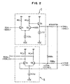
- Fig. 2 is a detailed circuit diagram showing an embodiment of the driver (transmitter circuit) D and the receiver (receiver circuit) R.
- the driver D comprises a balanced type differential amplifier which is formed by transistors Q1 and Q2 having the emitters tied together and connected to a current source Icsl, and corrector resistances Rc1 and Rc2, and also comprises an emitter-follower type transistor Q3 which has its emitter connected to a current source Ttt and amplifies output of the transistor Q2 and sends the amplified output through a terminal resistance RTA (RTB) to a transmission line L.
- a transmitting signal is input to the base of the transistor Q1.
- a threshold voltage VBB1 generated in the power unit contained in the device is supplied to the base of the transistor Q2.
- the receiver R comprises a balanced type differential amplifier which is formed by transistors Q4 and Q5 tied together and connected to a current source Ics2, and collector resistances Rc3 and Rc4, and a signal at the junction point to the transmission line L is supplied to the base of the transistor Q4, and a signal obtained with the resistances RBB1 and RBB2 serving as the voltage dividers between the output voltage of the transistor Q3 and the threshold voltage VTHB is input to the base of the other transistor Q5.
- a balanced type differential amplifier which is formed by transistors Q4 and Q5 tied together and connected to a current source Ics2, and collector resistances Rc3 and Rc4, and a signal at the junction point to the transmission line L is supplied to the base of the transistor Q4, and a signal obtained with the resistances RBB1 and RBB2 serving as the voltage dividers between the output voltage of the transistor Q3 and the threshold voltage VTHB is input to the base of the other transistor Q5.
- resistances RBB1 and RBB2 are set at the same resistance value.
- RTA and RTB The terminal resistances RTA and RTB and the resistances RBB1 and RBB2 are maintained in the following relation.
- RTA/RTB RBB1/RBB2
- RTB/RTA RBB2/RBB1
- This transmitting signal SRA1 is delayed by a delay time td of the transmission line L1 and transmitted to the input of the receiver R of the transmitter-receiver circuit TRB1 at the other end.
- a voltage VTHA1 obtained with the resistances RBB1 and RBB2 serving as voltage dividers between the voltage level of the transmitting signal SRA1 and the threshold voltage VTHA is applied to the base of the transistor Q5.
- the receiver R is formed by a differential amplifier, as shown in Fig. 3(h), if the receiving signal SRB1 from the other end is lower than the threshold voltage VTHA1, a signal RDB1 at LOW level is output, or if the receiving signal SRB1 is higher, the signal RDB1 at HIGH level is output.
- This transmitting signal SRB1 is delayed by a delay time td of the transmission line L1 and transmitted to the input of the receiver R of the transmitter-receiver circuit TRA1 at the other end.
- a threshold voltage VTHB1 produced by voltage-divider resistances RBB1 and RBB2 between the voltage level of the transmitting signal SRA1 and the thresold voltage VTHB is applied to the base of the transistor Q5.
- the threshold voltage VTHB1 applied to the base of the transistor Q5 is shifted to the HIGH level side by the amount corresponding to the amplitude of the transmitting signal SRA1.
- the receiver R as shown in Fig. 3(f) outputs a LOW level signal RDA1, if the receiving signal SRA1 is lower than the threshold voltage VTHB1 or the receiver R outputs a HIGH level signal RDA1 if the receiving signal SRA1 is higher than the threshold voltage VTHB1.
- the threshold voltage VTHA1 applied to the base of the transistor Q5 is shifted to the HIGH level side by the amount corresponding to the amplitude of the transmitting signal SRB1 of the same device as shown in Fig. 3(g).
- the transmitting signal SRA1 from the other device changes to the LOW level
- the receiving signal level is lower than the threshold voltage VTHA1, and therefore the signal RDA1 is changed to the LOW level as shown in Fig. 3(h).
- threshold voltages VTHB and VTHA generated by the power units in service in the transmitter-receiver circuits at the opposite ends of the transmission line are used as threshold voltages for logical decision on the receiving signal, even when the level of the receiving signal varies due to the potential difference Vg between the transmitter-receiver devices, the amount of variation is canceled out, so that a logical decision on the receiving signal can be made securely, and therefore the reliability of data transmission can be enhanced.
- Fig. 4 shows the effects achieved by the method mentioned above.
- the axis of abscissa represents changes in electric potential of the device at the opposite end as viewed from one device, while the axis of ordinates represents changes in the threshold level caused by changes in level of the receiving and transmitting signals.
- the letter H denotes a reception level when both the transmitting signal and the receiving signal are at HIGH level.
- the letter M denotes a reception level when the transmitting signal is at HIGH level and the receiving signal is at LOW level, or the transmitting signal is at LOW level and the receiving signal is at HIGH level.
- the letter L denotes a reception level when both the transmitting signal and the receiving signals are at LOW level.
- the code VTHH is the receiver's level of comparison when the transmitting signal is at HIGH level
- VTHL is the receiver's level of comparison when the transmitting signal is at LOW level.
- the codes VTHH' and VTHL' show changes in the receiver's comparison level when the threshold voltages are supplied from the device at the other end.
- the codes VTHH and VTHL indicate reception levels when the threshold voltages are self-supplied within the device.
- the receiver's comparison levels VTHH' and VTHL' change with the changes in the potential of the other device, and as a result, the relation between the reception level and the comparison levels is maintained normally for a wide range.
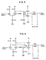
- Fig. 5 is a circuit diagram showing a second embodiment of the driver D, characterized by a complementary circuit configuration at the output stage.
- the output stage is formed by adding a transistor Q6 in complementary connection with the transistor Q3.
- the transistor Q3 is turned on to output a HIGH level signal, and the transistor Q6 is turned on to output a LOW level signal.
- This embodiment is arranged to let only an amount of current corresponding to output flow to the transmission line.
- a bias voltage is applied to the base of the transistor Q6 by output of the junction point between the current source Ics3, and diodes D1 and D2 connected in forward direction to the collector of the transistor Q2.
- This arrangement offers a special effect that power consumption can be reduced because only an amount of current corresponding to output is conducted to the transmission line by turning on the transistor Q6.
- Fig. 6 is a circuit showing a third embodiment of the driver D, characterized by the output stage formed by a complementary circuit including two NPN transistors.
- a diode D3 is connected between the collector of the transistor Q1 and the collector of a transistor Q7, and output at the junction point between the anode of the diode D3 and a current source Ics4 is input to the base of the transistor Q7.
- the transistor Q3 is turned on to output a HIGH level signal, and the transistor Q7 is turned on to output a LOW level signal, thereby letting only an amount of current corresponding to output flow to the transmission line L.
- a transmitter-receiver circuit configured as shown in Fig. 5 or 6
- the transmitter-receiver circuits placed against each other across the transmission line are sending signals of mutually different levels, such as in a combination of high-level (H) and low-level (L) or low-level (L) and high-level (H)
- a current flows through the transmission line L, so that electric power is consumed. If this power consumption occurs while no data is transmitted, this is quite a waste and needs to be eliminated.
- the transmitter-receiver circuits placed against each other are set such that the output voltages of those circuits are at the same level, namely, both at high (H) level or low (L) level.
- the driver Dn is of the same structure as before, but the receiver Rn is characterized by the provision of a function to detect a collision with transmitting signals from other transmitter-receiver circuits.
- a function to detect a collision with transmitting signals from other transmitter-receiver circuits In the transmission line of the bus structure, it is not allowed for the two transmitter-receiver circuits to send signals simultaneously. As a preventive measure, this function is provided which detects a collision of two transmitting signals in the transmission line of the bus structure.
- a receiver R1 of this embodiment includes first and second receivers R11 and R12 for comparing a signal SR1 sent out on the transmission line L with first and second threshold voltages VTH1 and VTH2 differing in voltage level by the amount corresponding to the amplitude of a signal sent out on the transmission line L, a third receiver R31 for comparing a signal SR1 sent out on the transmission line L with a third threshold voltage VTH3 of a level further higher by the amount corresponding to the amplitude of the signal than the level of the sum of the first and second threshold voltages VTH1 and VTH2, and outputting an alarm signal AL1 to invalidate the signal on the transmission line L when a signal SR1 higher than the third threshold voltage VTH3 appears on the transmission line, and EXCLUSIVE-OR circuits XOR1 and XOR2 for outputting a receiving signal RD1 sent through the transmission line L from another circuit by removing a signal sent from the driver D1 in the same circuit as the receiver R
- the output signal of the receiver R11 and a transmitting signal SD1 to transmit from the driver D are input to the EXCLUSIVE-OR circuit XOR1, while the output signal of the EXCLUSIVE-OR circuit XOR1 and the output signal of the receiver R21 are input to the EXCLUSIVE-OR circuit XOR2.
- the transmission line L is at LOW level, and therefore the output signals of the receivers R11 and R12 are at "0" (LOW) level as shown in Fig. 8(e).
- the output signal of the receiver R21 goes to the HIGH level.
- This signal is input to the EXCLUSIVE-OR circuit XOR2, but since the other input of the circuit XOR2 is at the HIGH level, the output remains at the LOW level.
- the threshold voltage is a voltage level used for making a decision of "HIGH” or "LOW” in logical circuits by TTL and MOS transistors.
- the threshold voltage VTH2 is set at an intermediate level between "HIGH” and "LOW” of the signal SR1 when a driver sends out a signal onto the transmission line L.
- This signal is input to the EXCLUSIVE-OR circuit XOR1. This means that both inputs of the circuit XOR1 are at “1” level, causing the output signal to go to "0" level. When output signal of the circuit XOR1 is “0”, the output signal of the circuit XOR2 at the next stage goes to the "1" level.
- the signal sent from the driver D2 of another transmitter-receiver circuit is extracted as the receiving signal RD1.
- the signal sent from the driver D2 of another transmitter-receiver circuit is received delayed by a delay time td due to the delay characteristic of the transmission line L as shown in Fig. 8.
- the signal AL1 is supplied to a circuit to accept the receiving signal as an alarm signal AL1 which invalidates the signal on the transmission line L.
- the threshold voltages VTH1, VTH2 and VTH3 are supplied from the power units for the transmitter circuits and the receiver circuits at the other end of the transmission line or the threshold voltages are produced from signals supplied, an alarm signal can be sent with higher accuracy.
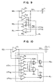
- Fig. 9 is a circuit diagram showing a second embodiment of related art of the current-driven type transmitter-receiver circuit, and a difference of this circuit from the circuit in Fig. 7 is that the receiving signal is reproduced by analog level comparison using a single threshold voltage VTH2.
- a voltage amplifier D12 to amplify the transmitting signal SD1 to a voltage signal twice as high as the amplitude when the signal is sent onto the transmission line L, and output of the voltage amplifier D12 is applied through a resistance ra1 to a receiver R41 formed of a comparator, a threshold voltage VTH2 (at the same voltage level as in Fig. 8) is applied through a resistance ra2 to the output side of a resistance ra1, and a voltage obtained with the resistances ra1 and ra2 serving as voltage-dividers between the threshold voltage VTH2 and the output voltage of the voltage amplifier D12 is used as a comparative reference voltage of the receiver R4.
- the driver D1 in the same circuit is not sending a signal SR1
- the comparative reference voltage of the receiver R41 is formed only by the threshold voltage VTH2, and depending on whether or not a signal higher than the threshold voltage VTH2 arrives, the receiving signal from another transmitter-receiver circuit is regenerated.
- the driver D1 in the same circuit is sending a signal SR1, as for the comparative reference voltage of the receiver R41, since the threshold voltage VTH2 is shifted to the HIGH level side by the output voltage of the voltage amplifier D12, the comparative reference voltage rises to the level same as the threshold voltage VTH1 shown in Fig. 8. Therefore, it is possible to distinguish a signal sent out from the device at this end and a signal received from the device at the other end of the transmission line, and regenerate only the transmitting signal from the other end.
- a collision of two or more transmitting signals can be detected in the same manner as in Fig. 7.
- Fig. 10 is a circuit diagram showing a third embodiment of related art of the current-driven type transmitter-receiver circuit, and a difference of this circuit from the circuit in Fig. 7 is that under the condition that another transmitter-receiver circuit is already sending a signal and the voltage level of the transmission line is higher than the threshold voltage VTH1, even when the driver D1 of the device at this end of the transmission line is not sending a signal, an alarm signal AL1 is output.
- the third embodiment of the transmit-receive circuit of related art comprises with an inverter N1 for inverting the input condition of a transmitting signal SD1, an AND gate for carrying out the logical AND of an output signal of the inverter N1 and output signals of the receivers R11 and R21, and an OR gate OG1 for outputting as an alarm signal AL1 a signal representing the result of ORing of an output signal of the AND gate AG1 and an output signal of the receiver R31.
- this embodiment it is possible to prevent three transmitting signals from occurring simultaneously. In other words, this embodiment offers a unique effect that different items of information on the transmission line can be avoided securely.
- Fig. 11 is a circuit diagram showing a fourth embodiment of the current-driven type transmitter-receiver circuit, a difference of this circuit from the circuit in Fig. 10 is that the regeneration of a receiving signal and the avoidance of signal collision are performed by analog level comparison.
- buffer amplifiers BF1 and BF2 for a transmitting signal SD1 are provided, output signals of those buffer amplifiers BF1 and BF2 are applied through resistances r1 and r3 to the comparative reference voltage input terminals (-) of receivers R11 and R31, and bias voltages VB1 and VB2 set to satisfy the relation shown in Fig. 12 are applied through resistances r2 and r4 to the comparative reference voltage input terminals (-) of the receivers R11 and R31.
- the bias voltage VB1 as indicated by "HL” in Fig. 12, is set at the same level as the amplitude level of a transmitting signal.
- the threshold voltage VTH1 input to the comparative reference input terminal (-) of the receiver R11 moves in a range of 0.5 to 1.5 times of the amplitude level of a transmitting signal according to the output level of the buffer amplifier BF1 as shown in Fig. 12.
- the threshold voltage VTH2 input to the comparative reference voltage input terminal (-) of the receiver R31 moves in a range two to three times the amplitude level of a transmitting signal according to the output level of the buffer amplifier BF2 as shown in Fig. 12.
- the HIGH level output of the buffer amplifier BF2 is added through the resistance r1 to the comparative reference voltage input terminal (-) of the receiver R11, so that the threshold voltage VTH1 rises to a value 1.5 times the amplitude level of a transmitting signal.
- the output signal RD1 of the receiver R11 is maintained at the LOW level.
- the voltage level of the transmission line L rises twice as high as before, thus exceeding the threshold voltage VTH1. Therefore, the output signal RD1 of the receiver R11 goes to the HIGH level. In other words, it is possible to extract a transmitting signal exclusive of a transmitting signal sent out by this transmitter-receiver circuit from among a composite signal including transmitting signals from this and other transmitter-receiver circuits.
- the threshold voltage VTH2 input to the comparative reference voltage input terminal (-) of the receiver R31 rises to 2.5 times as high as the amplitude level of a transmitting signal.
- the output signal of the receiver R31 is maintained at the LOW level.
- a transmission-reception circuit including a transmitter circuit and a receiver circuit connected to each end of a transmission line, for transmitting and receiving a signal to the receiver circuit and from the transmitter circuit at the other end of the transmission line, wherein power supply lines are laid at both the opposite ends of the transmission line, and a threshold voltage for logical decision on a signal received at the receiver circuit is supplied from a power unit used for the transmitter circuit and the receiver circuit at the other end.
- this invention is applied to communication between LSIs which have increased in the number of wires used, the number of wires between LSIs can be reduced for communication with high reliability.
- the receiver circuit comprises a first comparing means for comparing a signal sent out on the transmission line with first and second threshold voltages for logical decision on a signal, these threshold voltages differing in voltage level by the amount corresponding to the amplitude of a signal sent out on the transmission line, and a second comparing means for comparing a signal sent out on the transmission line with a third threshold voltage of a level further higher by the amount corresponding to the amplitude of the signal sent out on the transmission line than the level of the sum of the first and second threshold voltages, and outputting an alarm signal to invalidate the signal on the transmission line when a signal higher than the third threshold voltage appears on the transmission line.
- an alarm signal is output which invalidates the signal on the common transmission line.
- the output stage of the transmitter circuit is formed by a pair of switching elements connected in a complementary connection, power consumption in signal transmission can be cut down, and therefore this method is very economical. Above all, this method is very effective in reducing heat generation, when applied to LSIs.
Landscapes
- Engineering & Computer Science (AREA)
- Signal Processing (AREA)
- Computer Networks & Wireless Communication (AREA)
- Dc Digital Transmission (AREA)
- Small-Scale Networks (AREA)
- Bidirectional Digital Transmission (AREA)
Claims (4)
- Sende-/Empfangs-System mit einer Sendeschaltung (D) bei einer ersten Sende-/Empfangs-Vorrichtung (TRA) und einer Empfangsschaltung (R) bei einer zweiten Sende-/Empfangs-Vorrichtung (TRB), die mit gegenüberliegenden Enden einer Übertragungsleitung (L) verbunden sind, um Signale (SRA1, SRB1) von der Sendeschaltung (D) zur Empfangsschaltung (R) an den gegenüberliegenden Enden der Übertragungsleitung zu senden bzw. zu empfangen,
gekennzeichnet durch
eine Leistungseinheit (PSA) an der Sendeschaltung (D) am einen Ende der Übertragungsleitung (L), die eine Schwellenspannung (VTHA, VTHB) liefert, um den logischen Pegel eines von der Empfangsschaltung (R) am anderen Ende der Übertragungsleitung (L) empfangenen Signals zu entscheiden. - System nach Anspruch 1, bei dem die Ausgangsstufe der Sendeschaltung (D) durch Schaltelemente (Q3, Q6) gebildet wird, die komplementär verbunden sind.
- System nach Anspruch 1 oder 2, bei dem Ausgangsspannungen (SRA1, SRB1) der Sende-/Empfangs-Schaltungen (TRA1, TRA2), die jeweils eine Sendeschaltung (D) und eine Empfangsschaltung (R) aufweisen für die Übertragungsleitung auf den gleichen logischen Pegel gesetzt werden, wenn keine Kommunikation erfolgt.
- System nach einem der Ansprüche 1 bis 3, mit einer Einrichtung (Vg) zum Liefern eines Potenzialunterschieds zwischen der Leistungseinheit (PSA), die für die Sendeschaltung (D) verwendet wird, und der Leistungsschaltung (PSB), die für die Empfangsschaltung (R) verwendet wird.
Applications Claiming Priority (3)
| Application Number | Priority Date | Filing Date | Title |
|---|---|---|---|
| JP05179127A JP3137809B2 (ja) | 1993-07-20 | 1993-07-20 | 送受信回路 |
| JP179127/93 | 1993-07-20 | ||
| JP17912793 | 1993-07-20 |
Publications (3)
| Publication Number | Publication Date |
|---|---|
| EP0635954A2 EP0635954A2 (de) | 1995-01-25 |
| EP0635954A3 EP0635954A3 (de) | 1997-12-17 |
| EP0635954B1 true EP0635954B1 (de) | 2004-02-18 |
Family
ID=16060468
Family Applications (1)
| Application Number | Title | Priority Date | Filing Date |
|---|---|---|---|
| EP94110977A Expired - Lifetime EP0635954B1 (de) | 1993-07-20 | 1994-07-14 | Sende-Empfangsschaltungssystem |
Country Status (5)
| Country | Link |
|---|---|
| US (1) | US5499269A (de) |
| EP (1) | EP0635954B1 (de) |
| JP (1) | JP3137809B2 (de) |
| KR (1) | KR0140029B1 (de) |
| DE (1) | DE69433558T2 (de) |
Families Citing this family (27)
| Publication number | Priority date | Publication date | Assignee | Title |
|---|---|---|---|---|
| US5926509A (en) * | 1992-07-13 | 1999-07-20 | Cybex Computer Products Corporation | Twisted pair communicatons line system |
| US6377629B1 (en) * | 1994-01-05 | 2002-04-23 | Cybex Computer Products Corporation | Twisted pair communications line system |
| DE4421083C2 (de) * | 1994-06-16 | 1996-04-11 | Volkswagen Ag | Verfahren zur Überwachung einer seriellen Übertragung von digitalen Daten auf einer Ein-Draht-Multiplexverbindung zwischen untereinander kommunizierenden Signalverarbeitungsgeräten |
| KR0123204B1 (ko) * | 1994-12-30 | 1997-11-19 | 김주용 | 무선통신 단말기용 송수신 신호 스위칭 회로 |
| DE19523031A1 (de) * | 1995-06-08 | 1996-12-12 | Philips Patentverwaltung | System zum Übertragen von Daten über einen differentiellen Bus |
| US5729547A (en) * | 1996-02-07 | 1998-03-17 | Dutec, Inc. | Automatic driver/receiver control for half-duplex serial networks |
| US5912924A (en) * | 1996-08-15 | 1999-06-15 | Seeq Technology, Inc. | Bidirectional channels using common pins for transmit and receive paths |
| US5898678A (en) | 1996-09-25 | 1999-04-27 | Seeq Technology, Inc. | Method and apparatus for using synthetic preamable signals to awaken repeater |
| US5793815A (en) * | 1996-12-13 | 1998-08-11 | International Business Machines Corporation | Calibrated multi-voltage level signal transmission system |
| US6324602B1 (en) * | 1998-08-17 | 2001-11-27 | Integrated Memory Logic, Inc. | Advanced input/output interface for an integrated circuit device using two-level to multi-level signal conversion |
| US6522701B1 (en) | 1998-10-07 | 2003-02-18 | Conexant Systems, Inc. | Method and apparatus for extracting received digital data from a full-duplex point-to-point signaling channel using sampled-data techniques |
| US6184717B1 (en) * | 1998-12-09 | 2001-02-06 | Nortel Networks Limited | Digital signal transmitter and receiver using source based reference logic levels |
| US6188314B1 (en) | 1999-02-03 | 2001-02-13 | Trw Inc. | Energy distribution and communication system and method utilizing a communication message frame for a multi-device vehicle occupant protection system |
| EP1047149A3 (de) * | 1999-04-21 | 2003-02-12 | Matsushita Electric Industrial Co., Ltd. | Signalsender/Empfängergerät |
| JP3512168B2 (ja) * | 1999-04-21 | 2004-03-29 | 松下電器産業株式会社 | 信号送受信装置 |
| US6477592B1 (en) | 1999-08-06 | 2002-11-05 | Integrated Memory Logic, Inc. | System for I/O interfacing for semiconductor chip utilizing addition of reference element to each data element in first data stream and interpret to recover data elements of second data stream |
| US6744820B1 (en) | 2000-03-21 | 2004-06-01 | Trw Inc. | Communication system and method utilizing message frames having multiple thresholds for a multi-device vehicle occupant protection system |
| US6937664B1 (en) | 2000-07-18 | 2005-08-30 | Integrated Memory Logic, Inc. | System and method for multi-symbol interfacing |
| US6771675B1 (en) | 2000-08-17 | 2004-08-03 | International Business Machines Corporation | Method for facilitating simultaneous multi-directional transmission of multiple signals between multiple circuits using a single transmission line |
| JP3868776B2 (ja) * | 2001-08-28 | 2007-01-17 | 株式会社日立製作所 | 双方向データ送受信方法及びシステム |
| US7557790B2 (en) * | 2003-03-12 | 2009-07-07 | Samsung Electronics Co., Ltd. | Bus interface technology |
| JP4141884B2 (ja) * | 2003-04-17 | 2008-08-27 | 株式会社リコー | 信号伝送装置 |
| US8154995B2 (en) * | 2005-01-26 | 2012-04-10 | At&T Intellectual Property I, L.P. | System and method of managing digital data transmission |
| JP4648095B2 (ja) * | 2005-06-02 | 2011-03-09 | アラクサラネットワークス株式会社 | 信号伝送回路およびその調整方法 |
| JP2007116263A (ja) * | 2005-10-18 | 2007-05-10 | Orion Denki Kk | 電子装置及びデータ通信制御方法 |
| JP2010259060A (ja) * | 2009-04-22 | 2010-11-11 | Advantest Corp | ドライバ・コンパレータ回路およびそれを用いた試験装置 |
| JP5204040B2 (ja) * | 2009-06-09 | 2013-06-05 | アラクサラネットワークス株式会社 | 伝送回路およびパラメータ調整方法 |
Family Cites Families (13)
| Publication number | Priority date | Publication date | Assignee | Title |
|---|---|---|---|---|
| US3993867A (en) * | 1974-10-15 | 1976-11-23 | Motorola, Inc. | Digital single signal line full duplex method and apparatus |
| JPS5698052A (en) * | 1980-01-08 | 1981-08-07 | Fuji Facom Corp | Base band two-way simultaneous transmission circuit |
| JPS5922414B2 (ja) * | 1980-10-08 | 1984-05-26 | 富士通株式会社 | ラインドライバ回路 |
| US4573168A (en) * | 1984-08-31 | 1986-02-25 | Sperry Corporation | Balanced bidirectional or party line transceiver accommodating common-mode offset voltage |
| US4638473A (en) * | 1984-12-28 | 1987-01-20 | Gte Laboratories Incorporated | Two wire bidirectional digital transmission system |
| US4605864A (en) * | 1985-01-04 | 1986-08-12 | Advanced Micro Devices, Inc. | AFL (advanced fast logic) line driver circuit |
| US4860309A (en) * | 1986-09-17 | 1989-08-22 | Costello John F | Trinary bus communication system |
| DE3715588C1 (de) * | 1987-05-09 | 1988-09-08 | Gewerkschaft Eisenhuette Westfalia Gmbh, 4670 Luenen, De | |
| JPH0250537A (ja) * | 1988-08-11 | 1990-02-20 | Fujitsu Ltd | 双方向同時通信方式 |
| JPH0828750B2 (ja) * | 1989-11-10 | 1996-03-21 | 富士通株式会社 | レシーバ回路における自動閾値制御方式 |
| JPH03186033A (ja) * | 1989-12-15 | 1991-08-14 | Mitsubishi Electric Corp | 信号伝送方式 |
| JPH0752870B2 (ja) * | 1990-05-17 | 1995-06-05 | 日本電装株式会社 | 通信装置 |
| SG43345A1 (en) * | 1990-11-30 | 1997-10-17 | Yokogawa Electric Corp | Signal conditioner |
-
1993
- 1993-07-20 JP JP05179127A patent/JP3137809B2/ja not_active Expired - Fee Related
-
1994
- 1994-07-14 DE DE69433558T patent/DE69433558T2/de not_active Expired - Fee Related
- 1994-07-14 EP EP94110977A patent/EP0635954B1/de not_active Expired - Lifetime
- 1994-07-15 US US08/275,393 patent/US5499269A/en not_active Expired - Fee Related
- 1994-07-19 KR KR1019940017375A patent/KR0140029B1/ko not_active Expired - Fee Related
Also Published As
| Publication number | Publication date |
|---|---|
| KR950004643A (ko) | 1995-02-18 |
| JPH0738542A (ja) | 1995-02-07 |
| EP0635954A2 (de) | 1995-01-25 |
| EP0635954A3 (de) | 1997-12-17 |
| JP3137809B2 (ja) | 2001-02-26 |
| US5499269A (en) | 1996-03-12 |
| DE69433558D1 (de) | 2004-03-25 |
| DE69433558T2 (de) | 2004-12-16 |
| KR0140029B1 (ko) | 1998-07-01 |
Similar Documents
| Publication | Publication Date | Title |
|---|---|---|
| US5499269A (en) | Transmission-reception circuit | |
| EP0403147A2 (de) | Leistungsschnittstellenschaltung und Verfahren zur Prüfung einer solchen Schaltung | |
| US20060013331A1 (en) | Current mode differential transmission method and system for transmitting three units of data using four signal lines | |
| US4112253A (en) | Device for the transmission of push-pull signals across a two-wire line in full duplex operation | |
| EP0276277B1 (de) | Datenkommunikationssystem mit mitteln zur geräuschverringerung | |
| TW272344B (en) | System and method that provides simultaneous, bidirectional transfer of signals between integrated circuit devices | |
| JP3366007B2 (ja) | 二重冗長構成要素間で4本の信号経路を利用して情報を送信する装置及び方法 | |
| US5898729A (en) | Fault tolerant digital transmission system | |
| US6725304B2 (en) | Apparatus for connecting circuit modules | |
| US8245979B2 (en) | Centralized bus interface with single wire secondary distribution | |
| US6463496B1 (en) | Interface for an I2C bus | |
| EP2680504B1 (de) | Auf ein Serienübertragungssystem aufgebrachter Chip und zugehöriges betriebssicheres Verfahren | |
| US5311170A (en) | Method and system for making bipolar switching to protection channel | |
| US6714595B1 (en) | Signal transmission circuits that use multiple input signals to generate a respective transmit signal and methods of operating the same | |
| US4680431A (en) | Data network interface module with circuitry for disconnecting a module that has lost supply voltage | |
| US4866705A (en) | Data transmission system with means for distributing collision signals via the transmission line | |
| EP0785649B1 (de) | Verfahren und Vorrichtung zur Korrektur von Übertragungsfehlern und Erkennung von Fehlern während der Übertragung von Daten über ein Datenübertragungsmedium | |
| JP3497691B2 (ja) | 送受信回路 | |
| JP2002344428A (ja) | データ転送システム及びデータ転送方法 | |
| KR101021796B1 (ko) | M-pam 시그널링 방법 및 그에 따른 m-pam 드라이버, 수신기 | |
| US7446572B2 (en) | Method and system for a configurable Vcc reference and Vss reference differential current mode transmitter | |
| JPS60217747A (ja) | 回線切換回路 | |
| JPH0530087A (ja) | ドライバ・レシーバ | |
| JPH0662086A (ja) | ストローブ信号送受信装置 | |
| KR930012510A (ko) | 선박 자동화 제어용 통신모듈 |
Legal Events
| Date | Code | Title | Description |
|---|---|---|---|
| PUAI | Public reference made under article 153(3) epc to a published international application that has entered the european phase |
Free format text: ORIGINAL CODE: 0009012 |
|
| AK | Designated contracting states |
Kind code of ref document: A2 Designated state(s): DE FR GB |
|
| 17P | Request for examination filed |
Effective date: 19950202 |
|
| PUAL | Search report despatched |
Free format text: ORIGINAL CODE: 0009013 |
|
| AK | Designated contracting states |
Kind code of ref document: A3 Designated state(s): DE FR GB |
|
| 17Q | First examination report despatched |
Effective date: 20001228 |
|
| RTI1 | Title (correction) |
Free format text: TRANSMISSION-RECEPTION SYSTEM |
|
| GRAP | Despatch of communication of intention to grant a patent |
Free format text: ORIGINAL CODE: EPIDOSNIGR1 |
|
| RTI1 | Title (correction) |
Free format text: TRANSMISSION-RECEPTION SYSTEM |
|
| RTI1 | Title (correction) |
Free format text: TRANSMISSION-RECEPTION SYSTEM |
|
| GRAS | Grant fee paid |
Free format text: ORIGINAL CODE: EPIDOSNIGR3 |
|
| GRAA | (expected) grant |
Free format text: ORIGINAL CODE: 0009210 |
|
| AK | Designated contracting states |
Kind code of ref document: B1 Designated state(s): DE FR GB |
|
| REG | Reference to a national code |
Ref country code: GB Ref legal event code: FG4D |
|
| REF | Corresponds to: |
Ref document number: 69433558 Country of ref document: DE Date of ref document: 20040325 Kind code of ref document: P |
|
| PGFP | Annual fee paid to national office [announced via postgrant information from national office to epo] |
Ref country code: FR Payment date: 20040519 Year of fee payment: 11 |
|
| PG25 | Lapsed in a contracting state [announced via postgrant information from national office to epo] |
Ref country code: GB Free format text: LAPSE BECAUSE OF NON-PAYMENT OF DUE FEES Effective date: 20040714 |
|
| ET | Fr: translation filed | ||
| PLBE | No opposition filed within time limit |
Free format text: ORIGINAL CODE: 0009261 |
|
| STAA | Information on the status of an ep patent application or granted ep patent |
Free format text: STATUS: NO OPPOSITION FILED WITHIN TIME LIMIT |
|
| PG25 | Lapsed in a contracting state [announced via postgrant information from national office to epo] |
Ref country code: DE Free format text: LAPSE BECAUSE OF NON-PAYMENT OF DUE FEES Effective date: 20050201 |
|
| 26N | No opposition filed |
Effective date: 20041119 |
|
| GBPC | Gb: european patent ceased through non-payment of renewal fee |
Effective date: 20040714 |
|
| PG25 | Lapsed in a contracting state [announced via postgrant information from national office to epo] |
Ref country code: FR Free format text: LAPSE BECAUSE OF NON-PAYMENT OF DUE FEES Effective date: 20050731 |
|
| PG25 | Lapsed in a contracting state [announced via postgrant information from national office to epo] |
Ref country code: FR Free format text: LAPSE BECAUSE OF NON-PAYMENT OF DUE FEES Effective date: 20040731 |
|
| REG | Reference to a national code |
Ref country code: FR Ref legal event code: ST Effective date: 20110131 |