EP0637067A2 - Gravure par plasma utilisant du xénon - Google Patents
Gravure par plasma utilisant du xénon Download PDFInfo
- Publication number
- EP0637067A2 EP0637067A2 EP94303996A EP94303996A EP0637067A2 EP 0637067 A2 EP0637067 A2 EP 0637067A2 EP 94303996 A EP94303996 A EP 94303996A EP 94303996 A EP94303996 A EP 94303996A EP 0637067 A2 EP0637067 A2 EP 0637067A2
- Authority
- EP
- European Patent Office
- Prior art keywords
- etch
- etchant
- gas
- substrate
- volumetric flow
- Prior art date
- Legal status (The legal status is an assumption and is not a legal conclusion. Google has not performed a legal analysis and makes no representation as to the accuracy of the status listed.)
- Ceased
Links
Images
Classifications
-
- H—ELECTRICITY
- H10—SEMICONDUCTOR DEVICES; ELECTRIC SOLID-STATE DEVICES NOT OTHERWISE PROVIDED FOR
- H10P—GENERIC PROCESSES OR APPARATUS FOR THE MANUFACTURE OR TREATMENT OF DEVICES COVERED BY CLASS H10
- H10P50/00—Etching of wafers, substrates or parts of devices
- H10P50/20—Dry etching; Plasma etching; Reactive-ion etching
- H10P50/26—Dry etching; Plasma etching; Reactive-ion etching of conductive or resistive materials
- H10P50/264—Dry etching; Plasma etching; Reactive-ion etching of conductive or resistive materials by chemical means
- H10P50/266—Dry etching; Plasma etching; Reactive-ion etching of conductive or resistive materials by chemical means by vapour etching only
- H10P50/267—Dry etching; Plasma etching; Reactive-ion etching of conductive or resistive materials by chemical means by vapour etching only using plasmas
-
- C—CHEMISTRY; METALLURGY
- C23—COATING METALLIC MATERIAL; COATING MATERIAL WITH METALLIC MATERIAL; CHEMICAL SURFACE TREATMENT; DIFFUSION TREATMENT OF METALLIC MATERIAL; COATING BY VACUUM EVAPORATION, BY SPUTTERING, BY ION IMPLANTATION OR BY CHEMICAL VAPOUR DEPOSITION, IN GENERAL; INHIBITING CORROSION OF METALLIC MATERIAL OR INCRUSTATION IN GENERAL
- C23F—NON-MECHANICAL REMOVAL OF METALLIC MATERIAL FROM SURFACE; INHIBITING CORROSION OF METALLIC MATERIAL OR INCRUSTATION IN GENERAL; MULTI-STEP PROCESSES FOR SURFACE TREATMENT OF METALLIC MATERIAL INVOLVING AT LEAST ONE PROCESS PROVIDED FOR IN CLASS C23 AND AT LEAST ONE PROCESS COVERED BY SUBCLASS C21D OR C22F OR CLASS C25
- C23F4/00—Processes for removing metallic material from surfaces, not provided for in group C23F1/00 or C23F3/00
Definitions
- the present invention relates to processes for etching semiconductor wafers.
- Reactive ion etching processes are used in the fabrication of semiconductor and other devices with submicron sized features, such as integrated circuit chips. These processes are used to selectively etch a substrate, where portions of the substrate are protected by a patterned etch-resistant "resist" material, such as photoresist or oxide-hardmask. The resist protected portions form "features" on the substrate which become part of the integrated circuit being processed.
- Etching is effected by introducing a process gas into a chamber and generating a plasma in the chamber, to create an etch gas from the process gas. The etch gas etches the substrate to create a volatile etch byproduct compound, which is then removed from the chamber.
- the process gas comprises Cl2, BCl3 and optionally N2.
- a problem with this process gas is that relatively thick residues or deposits form on the chamber walls and on the resist material. Some of these deposits form because the etch gas chemically reacts with the resist material. The deposit on the chamber walls can flake off to form particles that contaminate the wafers. Further, the formation of excessive amounts of residue on the resist can undesirably increase the area protected by the resist material, rendering the processed wafer unsuitable for use.
- a deposited layer can also form on the sidewalls of the freshly etched channels in the substrate.
- This deposit serves as a "passivating” layer which hinders continued etching, thereby preventing "isotropic” etching or undercutting. Isotropic etching occurs when etching proceeds horizontally below the resist layer, instead of vertically through the uncoated portions, resulting in the lower portions of the features being inwardly sloped. Although vertical "anisotropic" etching is desirable, an excessive deposit of passivating layer on the sidewalls is difficult to clean. Thus, it is desirable to have an etching process that either produces less build-up of deposit, or which reduces build-up by etching the deposit layers during the etch process.
- High profile microloading causes the cross-sectional profile of the features formed in the substrate to vary as a function of the spacing between the features. It is desirable to have an etching process which provides features with a uniform cross-section regardless of the spacing between the features.
- the process gases In plasma etch processes, it is also desirable for the process gases to have a low ionization potential so that less energy is required to ionize the gases. It is also advantageous that the process gases have a wide range of excitation energies so that energy transfer reactions, which promote etching efficacy, can occur between the various gaseous species. Also, gases with low corrosivity are preferred so that the corrosive effect of the etch gas on the processing apparatus is minimized.
- the present invention is directed to a process that satisfies these needs.
- a substrate with grain boundaries and having a resist thereon is placed into an etch zone, and a process gas is introduced into the etch zone.
- the process gas lacks oxygen and comprises: (i) a primary etchant selected from the group consisting of chlorine, fluorine, and bromine; (ii) a secondary etchant suitable for etching grain boundaries in the substrate; and (iii) xenon.
- a gas passivator such as N2, HCl, CHF3, CF4, CH4, or mixtures thereof, can be added to the process gas.
- a substantially oxygen-free plasma is generated in the etch zone to form an etch gas from the process gas which selectively etches the substrate.
- the secondary etchant is also suitable for etching the surface oxide layer on the substrate, and more preferably the secondary etchant is selected from the group consisting of BCl3, SiCl4, CCl4, and mixtures thereof.
- the volumetric flow ratio of the primary etchant: secondary etchant:xenon is selected so that the substrate to resist etching selectivity ratio is greater than about 2.5.
- the flow ratio of secondary etchant to primary etchant is selected so that the rate of etching of the grain boundaries in the substrate is substantially the same as the rate of etching of the grains.
- the volumetric flow ratio secondary etchant to primary etchant is from about 0.1:1 to about 2:1, and more preferably from about 0.3:1 to about 0.5:1.
- the volumetric flow ratio of xenon-to-primary etchant is selected so that the substrate is etched substantially anisotropically.
- the xenon: primary etchant ratio is from about 0.1:1 to about 1:1, and more preferably from about 0.2:1 to about 0.5:1.
- the passivator:primary etchant ratio is less than about 1:1, and is more preferably less than about 0.6:1.
- the present invention is directed to a reactive ion etching process for etching a substrate having grain boundaries and a resist layer thereon.
- a process gas is introduced into an etching zone containing the substrate.
- the process gas is absent oxygen, and comprises: (i) a primary etchant selected from the group consisting of chlorine, fluorine and bromine; (ii) a secondary etchant suitable for etching grain boundaries in the substrate; and (iii) xenon.
- a substantially oxygen-free plasma is generated in the etch zone, to form an etch gas, from the process gas, which selectively etches the substrate.
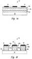
- the substrate 20 can be a semiconductor, metal, glass, or ceramic wafer 22 .
- the substrate 20 is a silicon or gallium arsenide wafer 22 having a plurality of layers 24 thereon.
- the layers 24 on the substrate can be metal, oxide, nitride, polysilicon or silicide layers.
- a resist material 26 such as photoresist or oxide hardmask, which is substantially resistant to etching is applied on top of the substrate layers.
- the resist 26 can be applied in a patterned overlay, as shown in Figure 1a.
- the resist 26 overlay protects portions of the substrate 20 so that, after the substrate 20 is etched, the protected portions of the substrate form features 28 that are part of the semiconductor device being processed.
- the features 28 can be laterally sized from about 0.5 to about 10 microns, and the spacings 30 between the features 28 can be on the order of at least about 0.5 microns.
- the substrate 20 has grains and grain boundaries.
- Each grain comprises a substantially ordered crystalline structure.
- the grain boundaries are the interfaces between the grains, which represent departures from the ordered structure of the grain, and which can contain impurities, such as oxide films.
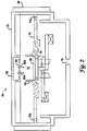
- a reaction apparatus 50 suitable for practicing the present invention comprises an etching chamber 52 having an etch zone 54 .
- the substrate 20 is typically placed on a cathode 56 in the etch chamber 52 .
- Process gas is introduced into the etch chamber 52 through the gas inlet 58 . Thereafter, the gas passes through a "showerhead" diffuser plate 60 which distributes the process gas in the etch zone 54 .
- a focus ring 62 can be used to substantially maintain the plasma in the etch zone 54 .
- a barrier or pumping plate 20 with a plurality of exhaust holes 72 therethrough, separates the etching chamber 52 into two zones, an etching zone 54 and a non-etching zone 74 .
- the exhaust holes 72 are in fluid communication with a vacuum pump through the exhaust port 76 for withdrawing spent process gas and volatile etch byproduct compounds from the etching chamber 52 .
- the reaction apparatus 50 can be a magnetically enhanced reactor, having a magnetic coil 80 around the etching chamber 52 to magnetically enhance the plasma formed in the etching zone 54 .
- a substrate 20 is placed on the cathode 56 , and the process gas is introduced through the gas inlet 58 into the etch zone 54 .
- a substantially oxygen-free plasma is generated in the etch zone 54 to form an etch gas from the process gas, which selectively etches the substrate.
- the flow of the etch gas is shown by the arrows 82 .
- the primary etchant is chlorine.
- the secondary etchant is selected from the group consisting of BCl3, SiCl4, CCl4, and mixtures thereof, and more preferably, the secondary etchant is BCl3.
- the process gas can further comprise a gas passivator selected from the group consisting of N2, HCl, CHF3, CF4, CH4, and mixtures thereof.
- the gas passivator is N2.
- the process gas can further comprise a chlorofluorocarbon, such as "FREON-14", manufactured by E.I. Du Pont de Nemours, Wilmington, Delaware.
- the composition of the process gas is controlled by adjusting the volumetric flow ratios of the primary etchant:secondary etchant:xenon.
- volumetric flow ratio it is meant the ratio of the volume per unit time of one gas to the volume per unit time of the second gas.
- the flow rates of the gases were measured using mass flow controllers. It is believed the three-part ratio of primary etchant to secondary etchant to xenon controls the etch rate, the amount of deposit found on the chamber walls, and the amount of deposition on the etch channel sidewalls.
- the volumetric flow ratio of primary etchant:secondary etchant:xenon is selected so that the substrate to resist etching selectivity ratio is greater than about 2.5.
- the etching selectivity ratio is defined as the rate at which the substrate is etched divided by the rate at which the resist is etched.
- the addition of xenon to the process gas provides an etch gas with a higher etching selectivity ratio than an etch gas without xenon. However, the addition of too much xenon slows down the rate of etching of the substrate.
- the volumetric flow ratio of secondary etchant to primary etchant is selected so that the rate of etching of the grain boundaries of the substrate is substantially the same as the rate of etching of the grains of the substrate.
- the volumetric flow ratio of secondary etchant to primary etchant is from about 0.1:1 to about 2:1, and more preferably from about 0.3:1 to about 0.5:1.
- the volumetric flow ratio of xenon to primary etchant is selected so that the substrate is etched substantially anisotropically, and at an etching rate substantially higher than the rate at which the resist is etched.
- the volumetric flow ratio of xenon:primary etchant is from about 0.1:1 to about 1:1, and more preferably from about 0.2:1 to about 0.5:1.
- the volumetric flow ratio of passivator to primary etchant is preferably less than about 1:1, and more preferably less than about 0.6:1.
- Insufficient gas passivator results in undercutting, i.e. etching of the layer below the resist material.
- Excess passivator results in slow etch rates and the formation of excessive deposits on the chamber walls and the freshly etched channel and sidewalls.
- the process gas is introduced at a rate which is sufficient that the rate of etching the substrate is greater than about 5,000 ⁇ per minute.
- the flow rate of the primary etchant is from about 10 to about 100 sccm, and more preferably, the flow rate is from about 40 to about 60 sccm.
- a substantially oxygen-free plasma is generated in the etch zone 54 to form an etch gas from the process gas.
- the etch gas etches the substrate 20 .
- the DC bias used to generate the plasma is generally from about -250 to about -450 Volts, and the amount of power typically from about 600 to about 1,000 Watts, more preferably from about 700 to about 900 Watts, and most preferably about 800 Watts.
- the plasma may be enhanced by a method such as electron cyclotron resonance, magnetically enhanced reactors and inductively coupled plasma.
- a magnetically enhanced ion reactor is used.
- the magnetic field in the reactor must be sufficiently strong to increase the density of the ions formed in the plasma, but not so strong as to induce charge-up damage, which would damage features such as CMOS gates.
- the magnetic field on the wafer surface is no more than 500 Gauss, typically it is from about 10 to about 100 Gauss, and more preferably from about 20 Gauss to about 80 Gauss.
- the chamber is maintained at a pressure of from about 1 mTorr to about 300 mTorr, preferably at least about 100 mTorr, and most preferably from about 100 to about 200 mTorr.
- the cathode can be heated using a heating source, such as a lamp, underneath the cathode.
- the cathode is preferably heated to temperatures sufficiently high to volatilize etching by-products, and sufficiently low that a thin layer of passivating deposit on the sidewalls of freshly etched channels is not volatilized.
- the cathode is heated to a temperature of about 50 to about 100°C, and more preferably from about 60°C to about 90°C.
- a flow of helium on the back of the wafer at a pressure of about 10 Torr can be used to control the temperature of the wafer.
- the chamber wall metal should be heated so that less deposit forms on the walls of the chamber.
- the chamber wall is heated to a temperature below the temperature of the substrate, and from about 45°C to about 85°C, and more preferably to about 65°C.
- the process conditions can be varied during the etching process. For example, when etching multiple layers of the substrate, typically the process has multiple stages. The process conditions for each stage can depend upon the layer that is being etched.
- the wafers used were silicon wafers of 200 mm (8 inch) diameter, coated successively with a 0.1 micron layer of titanium; 1 micron layer of aluminum, containing 0.5 percent copper; 0.04 micron layer of TiN; and resist in selected areas in a thickness of about 1.5 microns.
- a G-line photoresist material was used.
- the resist was placed on about 50 percent of the surface area of the wafer, to generate features of varying spacing and size. The highest density features were spaced apart by about 0.8 microns, and typically the features were about 0.6 microns wide.
- All the wafers were baked at 110°C for 30 minutes before etching. After the etching process was completed, the wafers were rinsed in distilled water and baked at 100°C for 30 minutes.
- SEM photos of the etched wafers were used to evaluate (i) photoresist remaining, (ii) sidewall smoothness, and (iii) amount of deposit remaining on the features, the latter either immediately after the plasma etch process, or after the dry/wet stripping operation described above. Etch rates were calculated by measuring the depth of the features in partially etched wafers.
- the progress of the etch was monitored by monitoring the composition of the gas withdrawn from the chamber using a optical omission technique.
- the composition of this gas changed, it signified that one layer has been etched through and the second layer was being etched.
- the composition of the process gases and other process conditions is changed to provide greater etching efficiency for the layer being etched.
- Example 2 To compare an etching process where xenon was added to the process gas to an etch process without xenon, two experiments were conducted as shown in Table 1. Only the BCl3 and xenon flow rates were changed between the runs. In Example 2, where xenon was added, the etch selectivity was higher and better profile microloading was observed. Also, in Example 2, the thickness of the photoresist layer remaining after etching was about 0.9 micrometer versus 0.8 micrometer remaining for Example 1. Thus, addition of xenon improved etch selectivity and profile microloading.
- the process conditions for Examples 3 and 4 are shown in Table 2.
- the wafers were etched in three stages: a preliminary etch, a main etch, and a final etch.
- the preliminary etch was time to breakthrough the overlayer of TiN so that the aluminum layer underneath was beginning to be etched.
- the main etch was conducted until the aluminum layer was etched through, or at "EPB" which stands for "end point at bottom.”
- the progress of the etch at all stages was monitored by monitoring the composition of gas withdrawn from the chamber using an optical emission technique.
- the EPB was determined at a point at which the content of aluminum in the gas withdrawn from the etching chamber substantially decreased.
- the final etch was timed so that the underlayer of TiN was etched.
- Examples 3 and 4 demonstrate that the addition of xenon in the main etching step, provides a process with less deposit formation and provides a higher photoresist to metal etching selectivity ratio.
- the primary etchant:secondary etchant:xenon ratio was varied using a factorial design study involving a L9 (34) orthogonal matrix.
- Three levels or values were selected for four process variables, power, Xe:Cl2 ratio, N2:Cl2 ratio, and HCl:Cl2 ratio, as shown in Table 3.
- TABLE 3 L9 (34) ORTHOGONAL MATRIX CONDITIONS Factors Level I II III Power (watts) 700 800 900 Xe/Cl2 0.5 1.0 1.5 N2/Cl2 0.2 0.6 1.0 HCl/Cl2 0.0 0.15 0.3
- the pressure was maintained at 200 mTorr and the magnetic field maintained at 20 Gauss.
- the cathode temperature was maintained at 80°C, and chamber wall temperature at 65°C.
- Helium was flowed at a pressure of 10 Torr on the backside of the wafer.
- the flow rate of the chlorine was maintained at 80 sccm, and the BCl3 flow rate was maintained constant at about 9% of the combined flow rate of all the process gases.
- Example 5 with a power level of 700 watts, a xenon:chlorine ratio of 0.5, a nitrogen:chlorine ratio 0.2, and a HCl:chlorine ratio 0.2, provided the best results as measured by residue remaining after the stripping operation, roughness of the sidewalls of the features and etch selectivity ratio.
- the critical distance measurements correspond to the width of the smallest feature in the center and in the edge of the wafer.
- the width of the smallest feature of these wafers should be about 0.6 microns. However, widths smaller than 0.6 microns were measured by scanning electron microscopy. The critical distance measurements were found to decrease with increasing power levels and increasing Xe:Cl2 ratio.
- Example 15 comprised of the prior art Cl2/BCl3/N2 process gas composition, was used as a baseline for comparison with the results of xenon containing examples.
- Examples 16-27 were run to attempt to reduce the roughness in the sidewalls 90 of the features 28 , and to reduce the amount of deposit 92 in the regions of the wafer with numerous closely spaced features.
- Example 16 xenon replaced the BCl3 of Example 15, providing thinner sidewall deposition.
- Example 17 BCl3 was added to the process condition of Example 16, to show that BCl3 is necessary to remove the residue.
- the removal of xenon in Example 18, resulted in high residue formation.
- Example 19 the amount of chlorine was decreased, and the magnetic field was increased, resulting in less residue formation.
- Example 20 reducing the power level somewhat improved the sidewall roughness.
- Example 21 the power level was further reduced, causing undercutting during etching of the Ti layer.
- Example 22 a lower temperature was maintained at the cathode, however, this resulted in more residue in the dense areas of the wafer.
- Example 23 CF4 was added causing more residue to accumulate.
- Example 24 the addition of HCl caused more deposit to accumulate.
- Example 25 the amount of nitrogen was increased, resulting in enhanced profile microloading.
- Example 26 increasing the temperature of the cathode did not decrease residue formation.
- Example 27 reducing the pressure caused more residue to form in the open areas of the substrate.
- a process according to the present invention has a high etch rate (greater than 5,000 ⁇ per minute), good substrate to resist etch selectivity, and satisfactory sidewall profile of the features formed below the resist. Also, the process provides substantially reduced amounts of deposit on the chamber walls and on the sidewalls of the freshly etched channels. Furthermore, existing reactive-ion etching equipment can be used.
Landscapes
- Chemical & Material Sciences (AREA)
- Engineering & Computer Science (AREA)
- Materials Engineering (AREA)
- Mechanical Engineering (AREA)
- Metallurgy (AREA)
- Organic Chemistry (AREA)
- Drying Of Semiconductors (AREA)
- ing And Chemical Polishing (AREA)
Applications Claiming Priority (2)
| Application Number | Priority Date | Filing Date | Title |
|---|---|---|---|
| US78131 | 1993-06-16 | ||
| US08/078,131 US5384009A (en) | 1993-06-16 | 1993-06-16 | Plasma etching using xenon |
Publications (2)
| Publication Number | Publication Date |
|---|---|
| EP0637067A2 true EP0637067A2 (fr) | 1995-02-01 |
| EP0637067A3 EP0637067A3 (fr) | 1995-05-17 |
Family
ID=22142103
Family Applications (1)
| Application Number | Title | Priority Date | Filing Date |
|---|---|---|---|
| EP94303996A Ceased EP0637067A3 (fr) | 1993-06-16 | 1994-06-03 | Gravure par plasma utilisant du xénon. |
Country Status (3)
| Country | Link |
|---|---|
| US (1) | US5384009A (fr) |
| EP (1) | EP0637067A3 (fr) |
| JP (2) | JP3574680B2 (fr) |
Cited By (5)
| Publication number | Priority date | Publication date | Assignee | Title |
|---|---|---|---|---|
| WO1998028785A1 (fr) * | 1996-12-20 | 1998-07-02 | Lam Research Corporation | Procede pour ameliorer la selectivite par photoresist et reduire les effets de charge de la vitesse de gravure |
| GB2337361A (en) * | 1998-05-06 | 1999-11-17 | United Microelectronics Corp | A method of etching a tantalum oxide layer in the fabrication of a DRAM |
| EP0917187A3 (fr) * | 1997-11-14 | 2000-01-26 | Siemens Aktiengesellschaft | Méthode de gravure d'un film mince de métal essentiellement composé d'aluminium |
| US6090304A (en) * | 1997-08-28 | 2000-07-18 | Lam Research Corporation | Methods for selective plasma etch |
| EP1160849A3 (fr) * | 2000-05-30 | 2003-07-02 | Sharp Kabushiki Kaisha | Procédé de gravure plasma anisotrope utilisant un gas fluoré non chlorofluorocarboné |
Families Citing this family (37)
| Publication number | Priority date | Publication date | Assignee | Title |
|---|---|---|---|---|
| JP3009975B2 (ja) * | 1992-11-30 | 2000-02-14 | シャープ株式会社 | シリコン薄膜のドライエッチング方法 |
| JPH07130702A (ja) * | 1993-11-08 | 1995-05-19 | Fujitsu Ltd | 白金又はパラジウムよりなる金属膜のパターニング方法 |
| US5545289A (en) * | 1994-02-03 | 1996-08-13 | Applied Materials, Inc. | Passivating, stripping and corrosion inhibition of semiconductor substrates |
| US5552124A (en) * | 1994-06-22 | 1996-09-03 | Applied Materials, Inc. | Stationary focus ring for plasma reactor |
| US5607599A (en) * | 1994-11-17 | 1997-03-04 | Kabushiki Kaisha Toshiba | Method of processing a magnetic thin film |
| JP3484332B2 (ja) | 1997-11-11 | 2004-01-06 | Tdk株式会社 | 薄膜磁気ヘッドの製造方法 |
| US6797188B1 (en) | 1997-11-12 | 2004-09-28 | Meihua Shen | Self-cleaning process for etching silicon-containing material |
| US6136211A (en) * | 1997-11-12 | 2000-10-24 | Applied Materials, Inc. | Self-cleaning etch process |
| US6872322B1 (en) | 1997-11-12 | 2005-03-29 | Applied Materials, Inc. | Multiple stage process for cleaning process chambers |
| US5970376A (en) * | 1997-12-29 | 1999-10-19 | Taiwan Semiconductor Manufacturing Company, Ltd. | Post via etch plasma treatment method for forming with attenuated lateral etching a residue free via through a silsesquioxane spin-on-glass (SOG) dielectric layer |
| US6177337B1 (en) | 1998-01-06 | 2001-01-23 | International Business Machines Corporation | Method of reducing metal voids in semiconductor device interconnection |
| US6228775B1 (en) | 1998-02-24 | 2001-05-08 | Micron Technology, Inc. | Plasma etching method using low ionization potential gas |
| US6544429B1 (en) | 1999-03-25 | 2003-04-08 | Applied Materials Inc. | Enhancement of silicon oxide etch rate and substrate selectivity with xenon addition |
| US6797189B2 (en) | 1999-03-25 | 2004-09-28 | Hoiman (Raymond) Hung | Enhancement of silicon oxide etch rate and nitride selectivity using hexafluorobutadiene or other heavy perfluorocarbon |
| US6291357B1 (en) * | 1999-10-06 | 2001-09-18 | Applied Materials, Inc. | Method and apparatus for etching a substrate with reduced microloading |
| US6527968B1 (en) | 2000-03-27 | 2003-03-04 | Applied Materials Inc. | Two-stage self-cleaning silicon etch process |
| US6440864B1 (en) | 2000-06-30 | 2002-08-27 | Applied Materials Inc. | Substrate cleaning process |
| US6547979B1 (en) * | 2000-08-31 | 2003-04-15 | Micron Technology, Inc. | Methods of enhancing selectivity of etching silicon dioxide relative to one or more organic substances; and plasma reaction chambers |
| US6692903B2 (en) | 2000-12-13 | 2004-02-17 | Applied Materials, Inc | Substrate cleaning apparatus and method |
| US6555166B2 (en) | 2001-06-29 | 2003-04-29 | International Business Machines | Method for reducing the microloading effect in a chemical vapor deposition reactor |
| US7374696B2 (en) * | 2003-02-14 | 2008-05-20 | Applied Materials, Inc. | Method and apparatus for removing a halogen-containing residue |
| US20040195208A1 (en) * | 2003-02-15 | 2004-10-07 | Pavel Elizabeth G. | Method and apparatus for performing hydrogen optical emission endpoint detection for photoresist strip and residue removal |
| US20040219790A1 (en) * | 2003-04-30 | 2004-11-04 | Wilson Aaron R | Etching methods, RIE methods, and methods of increasing the stability of photoresist during RIE |
| US20040224524A1 (en) * | 2003-05-09 | 2004-11-11 | Applied Materials, Inc. | Maintaining the dimensions of features being etched on a lithographic mask |
| US7147122B2 (en) * | 2004-03-11 | 2006-12-12 | Crown Packaging Technology, Inc. | Easy open can end |
| JP4620964B2 (ja) * | 2004-04-20 | 2011-01-26 | パナソニック株式会社 | 金属膜のパターン形成方法 |
| US20060102197A1 (en) * | 2004-11-16 | 2006-05-18 | Kang-Lie Chiang | Post-etch treatment to remove residues |
| US8278222B2 (en) * | 2005-11-22 | 2012-10-02 | Air Products And Chemicals, Inc. | Selective etching and formation of xenon difluoride |
| US20070117396A1 (en) * | 2005-11-22 | 2007-05-24 | Dingjun Wu | Selective etching of titanium nitride with xenon difluoride |
| US8118946B2 (en) * | 2007-11-30 | 2012-02-21 | Wesley George Lau | Cleaning process residues from substrate processing chamber components |
| US8809196B2 (en) * | 2009-01-14 | 2014-08-19 | Tokyo Electron Limited | Method of etching a thin film using pressure modulation |
| CA2690697A1 (fr) * | 2009-01-27 | 2010-07-27 | Air Products And Chemicals, Inc. | Gravure selective et formation de difluorure de xenon |
| US9478428B2 (en) | 2010-10-05 | 2016-10-25 | Skyworks Solutions, Inc. | Apparatus and methods for shielding a plasma etcher electrode |
| US20120083129A1 (en) | 2010-10-05 | 2012-04-05 | Skyworks Solutions, Inc. | Apparatus and methods for focusing plasma |
| US9852924B1 (en) * | 2016-08-24 | 2017-12-26 | Lam Research Corporation | Line edge roughness improvement with sidewall sputtering |
| FR3086462A1 (fr) | 2018-09-21 | 2020-03-27 | Stmicroelectronics (Crolles 2) Sas | Procede de fabrication d'un composant electronique |
| JP7325256B2 (ja) * | 2019-08-05 | 2023-08-14 | 東京エレクトロン株式会社 | プラズマ処理装置 |
Family Cites Families (18)
| Publication number | Priority date | Publication date | Assignee | Title |
|---|---|---|---|---|
| US4190488A (en) * | 1978-08-21 | 1980-02-26 | International Business Machines Corporation | Etching method using noble gas halides |
| JPS56137367A (en) * | 1980-03-28 | 1981-10-27 | Ricoh Co Ltd | Jam detecting and processing system for copying machine |
| JPS56137637A (en) * | 1980-03-31 | 1981-10-27 | Chiyou Lsi Gijutsu Kenkyu Kumiai | Etching of aluminum film |
| US4468285A (en) * | 1983-12-22 | 1984-08-28 | Advanced Micro Devices, Inc. | Plasma etch process for single-crystal silicon with improved selectivity to silicon dioxide |
| US5108543A (en) * | 1984-11-07 | 1992-04-28 | Hitachi, Ltd. | Method of surface treatment |
| JPS62111432A (ja) * | 1985-11-08 | 1987-05-22 | Fujitsu Ltd | 半導体装置の製造方法 |
| US4789426A (en) * | 1987-01-06 | 1988-12-06 | Harris Corp. | Process for performing variable selectivity polysilicon etch |
| US4786359A (en) * | 1987-06-24 | 1988-11-22 | Tegal Corporation | Xenon enhanced plasma etch |
| JPH0265132A (ja) * | 1988-08-30 | 1990-03-05 | Sony Corp | ドライエッチング方法 |
| US5030319A (en) * | 1988-12-27 | 1991-07-09 | Kabushiki Kaisha Toshiba | Method of oxide etching with condensed plasma reaction product |
| US4949350A (en) * | 1989-07-17 | 1990-08-14 | Bell Communications Research, Inc. | Surface emitting semiconductor laser |
| US5034344A (en) * | 1989-07-17 | 1991-07-23 | Bell Communications Research, Inc. | Method of making a surface emitting semiconductor laser |
| JPH0378229A (ja) * | 1989-08-21 | 1991-04-03 | Matsushita Electron Corp | プラズマエッチング方法 |
| US5002632A (en) * | 1989-11-22 | 1991-03-26 | Texas Instruments Incorporated | Method and apparatus for etching semiconductor materials |
| JP3092185B2 (ja) * | 1990-07-30 | 2000-09-25 | セイコーエプソン株式会社 | 半導体装置の製造方法 |
| US5202291A (en) * | 1990-09-26 | 1993-04-13 | Intel Corporation | High CF4 flow-reactive ion etch for aluminum patterning |
| JPH05234959A (ja) * | 1991-08-16 | 1993-09-10 | Hitachi Ltd | ドライエッチング方法及びドライエッチング装置 |
| JPH05326515A (ja) * | 1992-05-19 | 1993-12-10 | Fujitsu Ltd | 半導体装置の製造方法 |
-
1993
- 1993-06-16 US US08/078,131 patent/US5384009A/en not_active Expired - Fee Related
-
1994
- 1994-06-03 EP EP94303996A patent/EP0637067A3/fr not_active Ceased
- 1994-06-16 JP JP13450894A patent/JP3574680B2/ja not_active Expired - Fee Related
-
2004
- 2004-04-23 JP JP2004128872A patent/JP2004247755A/ja active Pending
Cited By (7)
| Publication number | Priority date | Publication date | Assignee | Title |
|---|---|---|---|---|
| WO1998028785A1 (fr) * | 1996-12-20 | 1998-07-02 | Lam Research Corporation | Procede pour ameliorer la selectivite par photoresist et reduire les effets de charge de la vitesse de gravure |
| US5883007A (en) * | 1996-12-20 | 1999-03-16 | Lam Research Corporation | Methods and apparatuses for improving photoresist selectivity and reducing etch rate loading |
| US6090304A (en) * | 1997-08-28 | 2000-07-18 | Lam Research Corporation | Methods for selective plasma etch |
| EP0917187A3 (fr) * | 1997-11-14 | 2000-01-26 | Siemens Aktiengesellschaft | Méthode de gravure d'un film mince de métal essentiellement composé d'aluminium |
| GB2337361A (en) * | 1998-05-06 | 1999-11-17 | United Microelectronics Corp | A method of etching a tantalum oxide layer in the fabrication of a DRAM |
| GB2337361B (en) * | 1998-05-06 | 2000-03-29 | United Microelectronics Corp | Method of etching tantalum oxide layer |
| EP1160849A3 (fr) * | 2000-05-30 | 2003-07-02 | Sharp Kabushiki Kaisha | Procédé de gravure plasma anisotrope utilisant un gas fluoré non chlorofluorocarboné |
Also Published As
| Publication number | Publication date |
|---|---|
| JP2004247755A (ja) | 2004-09-02 |
| JPH0758079A (ja) | 1995-03-03 |
| JP3574680B2 (ja) | 2004-10-06 |
| EP0637067A3 (fr) | 1995-05-17 |
| US5384009A (en) | 1995-01-24 |
Similar Documents
| Publication | Publication Date | Title |
|---|---|---|
| US5384009A (en) | Plasma etching using xenon | |
| US5354417A (en) | Etching MoSi2 using SF6, HBr and O2 | |
| KR101468614B1 (ko) | 쓰루 기판 비아 측벽 및 깊게 에칭된 피쳐들을 스무싱하기 위한 사후 에칭 반응성 플라즈마 밀링 | |
| US6380095B1 (en) | Silicon trench etch using silicon-containing precursors to reduce or avoid mask erosion | |
| US5387556A (en) | Etching aluminum and its alloys using HC1, C1-containing etchant and N.sub.2 | |
| US6287978B1 (en) | Method of etching a substrate | |
| US6090717A (en) | High density plasma etching of metallization layer using chlorine and nitrogen | |
| US4855017A (en) | Trench etch process for a single-wafer RIE dry etch reactor | |
| US4784720A (en) | Trench etch process for a single-wafer RIE dry etch reactor | |
| US5843847A (en) | Method for etching dielectric layers with high selectivity and low microloading | |
| EP0482519B1 (fr) | Procédé d'attaque de matériaux à base d'oxydes | |
| US20080057729A1 (en) | Etch methods to form anisotropic features for high aspect ratio applications | |
| JP4907827B2 (ja) | ポリシリコンのエッチングの均一性を向上し、エッチング速度の変動を低減するための方法 | |
| EP0819786A2 (fr) | Procédé d'attaque pour le silicium monocristallin | |
| US20070202700A1 (en) | Etch methods to form anisotropic features for high aspect ratio applications | |
| US5453156A (en) | Anisotropic polysilicon plasma etch using fluorine gases | |
| EP1087421A2 (fr) | Procédé et appareil pour l'obtention d'un plasma stable | |
| US5880033A (en) | Method for etching metal silicide with high selectivity to polysilicon | |
| US5346585A (en) | Use of a faceted etch process to eliminate stringers | |
| EP0820093A1 (fr) | Gravure d'une couche antiréfléchissante organique d'un substrat | |
| US6756314B2 (en) | Method for etching a hard mask layer and a metal layer | |
| US6383941B1 (en) | Method of etching organic ARCs in patterns having variable spacings | |
| US5908320A (en) | High selectivity BPSG:TiSi2 contact etch process | |
| JPH11111677A (ja) | 半導体装置の製造方法 | |
| EP1198822B1 (fr) | Nouvelles methodologies permettant de reduire la sensibilite d'un traitement aux conditions prevalant dans la chambre |
Legal Events
| Date | Code | Title | Description |
|---|---|---|---|
| PUAI | Public reference made under article 153(3) epc to a published international application that has entered the european phase |
Free format text: ORIGINAL CODE: 0009012 |
|
| AK | Designated contracting states |
Kind code of ref document: A2 Designated state(s): DE FR GB IT NL |
|
| PUAL | Search report despatched |
Free format text: ORIGINAL CODE: 0009013 |
|
| AK | Designated contracting states |
Kind code of ref document: A3 Designated state(s): DE FR GB IT NL |
|
| 17P | Request for examination filed |
Effective date: 19950628 |
|
| 17Q | First examination report despatched |
Effective date: 19950921 |
|
| STAA | Information on the status of an ep patent application or granted ep patent |
Free format text: STATUS: THE APPLICATION HAS BEEN REFUSED |
|
| 18R | Application refused |
Effective date: 19980827 |