EP0637470A2 - Rückschicht für einen Anordnung von akustischen Wandler - Google Patents
Rückschicht für einen Anordnung von akustischen Wandler Download PDFInfo
- Publication number
- EP0637470A2 EP0637470A2 EP94305729A EP94305729A EP0637470A2 EP 0637470 A2 EP0637470 A2 EP 0637470A2 EP 94305729 A EP94305729 A EP 94305729A EP 94305729 A EP94305729 A EP 94305729A EP 0637470 A2 EP0637470 A2 EP 0637470A2
- Authority
- EP
- European Patent Office
- Prior art keywords
- electrical
- conductors
- acoustic
- layers
- backing layer
- Prior art date
- Legal status (The legal status is an assumption and is not a legal conclusion. Google has not performed a legal analysis and makes no representation as to the accuracy of the status listed.)
- Withdrawn
Links
Images
Classifications
-
- B—PERFORMING OPERATIONS; TRANSPORTING
- B06—GENERATING OR TRANSMITTING MECHANICAL VIBRATIONS IN GENERAL
- B06B—METHODS OR APPARATUS FOR GENERATING OR TRANSMITTING MECHANICAL VIBRATIONS OF INFRASONIC, SONIC, OR ULTRASONIC FREQUENCY, e.g. FOR PERFORMING MECHANICAL WORK IN GENERAL
- B06B1/00—Methods or apparatus for generating mechanical vibrations of infrasonic, sonic, or ultrasonic frequency
- B06B1/02—Methods or apparatus for generating mechanical vibrations of infrasonic, sonic, or ultrasonic frequency making use of electrical energy
- B06B1/06—Methods or apparatus for generating mechanical vibrations of infrasonic, sonic, or ultrasonic frequency making use of electrical energy operating with piezoelectric effect or with electrostriction
- B06B1/0644—Methods or apparatus for generating mechanical vibrations of infrasonic, sonic, or ultrasonic frequency making use of electrical energy operating with piezoelectric effect or with electrostriction using a single piezoelectric element
- B06B1/0662—Methods or apparatus for generating mechanical vibrations of infrasonic, sonic, or ultrasonic frequency making use of electrical energy operating with piezoelectric effect or with electrostriction using a single piezoelectric element with an electrode on the sensitive surface
- B06B1/0681—Methods or apparatus for generating mechanical vibrations of infrasonic, sonic, or ultrasonic frequency making use of electrical energy operating with piezoelectric effect or with electrostriction using a single piezoelectric element with an electrode on the sensitive surface and a damping structure
- B06B1/0685—Methods or apparatus for generating mechanical vibrations of infrasonic, sonic, or ultrasonic frequency making use of electrical energy operating with piezoelectric effect or with electrostriction using a single piezoelectric element with an electrode on the sensitive surface and a damping structure on the back only of piezoelectric elements
-
- B—PERFORMING OPERATIONS; TRANSPORTING
- B06—GENERATING OR TRANSMITTING MECHANICAL VIBRATIONS IN GENERAL
- B06B—METHODS OR APPARATUS FOR GENERATING OR TRANSMITTING MECHANICAL VIBRATIONS OF INFRASONIC, SONIC, OR ULTRASONIC FREQUENCY, e.g. FOR PERFORMING MECHANICAL WORK IN GENERAL
- B06B1/00—Methods or apparatus for generating mechanical vibrations of infrasonic, sonic, or ultrasonic frequency
- B06B1/02—Methods or apparatus for generating mechanical vibrations of infrasonic, sonic, or ultrasonic frequency making use of electrical energy
- B06B1/06—Methods or apparatus for generating mechanical vibrations of infrasonic, sonic, or ultrasonic frequency making use of electrical energy operating with piezoelectric effect or with electrostriction
- B06B1/0607—Methods or apparatus for generating mechanical vibrations of infrasonic, sonic, or ultrasonic frequency making use of electrical energy operating with piezoelectric effect or with electrostriction using multiple elements
- B06B1/0622—Methods or apparatus for generating mechanical vibrations of infrasonic, sonic, or ultrasonic frequency making use of electrical energy operating with piezoelectric effect or with electrostriction using multiple elements on one surface
- B06B1/0629—Square array
Definitions
- This invention relates to acoustic transducer arrays, and more Particularly, to a laminated backing layer for use with such arrays to electrically connect the array to a circuit element and to substantially eliminate spurious acoustic reflections caused by the array.
- Ultrasonic imaging systems are widely used to produce images of internal structure of a specimen or target of interest.
- a diagnostic ultrasonic imaging system for medical use forms images of internal tissues of a human body by electrically exciting an acoustic transducer element or an array of acoustic transducer elements to generate short ultrasonic pulses that are caused to travel into the body. Echoes from the tissues are received by the acoustic transducer element or elements and are converted into electrical signals.
- circuit element such as a printed circuit board, flexible cable or semiconductor, receives the electrical signals. The electrical signals are amplified and used to form a cross-sectional image of the tissues.
- the acoustic transducer which radiates the ultrasonic pulses is provided with a plurality of piezoelectric elements arranged in an array with a predetermined pitch.
- the array is generally one or two-dimensional. By reducing the pitch of the piezoelectric elements in the array, and increasing the number of elements, the resolution of the image can be increased.
- An operator of the imaging system can control the phase of the electronic pulses applied to the respective piezoelectric elements in order to vary the direction of the output ultrasonic wave beam or its focus. In this way, the operator can "steer" the direction of the ultrasonic wave in order to illuminate desired portions of the human body without needing to physically manipulate the position of the transducer.
- acoustic waves are transmitted both from the front surface facing the imaging target and the rear surface of the element. It is desirable that the acoustic energy from the rear surface be substantially attenuated so that the image resolution is not adversely affected. If not attenuated, the rearward travelling acoustic signals can reflect off the circuit element and return to the transducer surface, causing a degradation of the desired electrical signal.
- a backing layer of an acoustically attenuating material is disposed between the piezoelectric elements and the circuit element to attenuate the undesired acoustic energy from the rear surface of the piezoelectric element.
- this backing layer would have an acoustic impedance matched to the impedance of the piezoelectric elements so that a substantial portion of the acoustic energy at the rear surface of the piezoelectric element is coupled into the backing layer.
- a problem with the use of a backing layer between the piezoelectric element and the circuit element is that of providing electrical interconnection between the particular piezoelectric elements and the associated circuit elements.
- the interconnection problem is more difficult for two-dimensional arrays of more than three rows and columns of piezoelectric elements, since the internal elements will not have an exposed edge that accommodates electrical connection.
- electrical interconnection between the individual piezoelectric elements and the electric circuit which receives and processes the electrical signals is generally made in the z-axis direction perpendicular to the array.
- the pitch between the elements decreases, it becomes increasingly difficult to fabricate this interconnection.
- a secondary problem which increases the difficulty of forming the electrical interconnections is that of undesired cross-talk.
- Cross-talk is defined as unintended interference between adjacent signal conductors, which occurs via capacitive or inductive coupling.
- cross-talk can be minimized or eliminated through shielding of the conductive element. While a shield provided around the electrical conductors which form the interconnections through the backing layer would mitigate the cross-talk problem, the shield increases the difficulty of providing the conductors through the solid backing layer.
- Such a technique should provide for the outputted acoustic energy from the rear surface of the piezoelectric element to be fully attenuated so that there are substantially no reflections of such energy back into the transducer element.
- the technique should also permit relative ease of manufacture and ready adaptability for large transducer arrays having high numbers of piezoelectric elements with relatively small pitch.
- this invention provides an acoustic transducer for transmitting acoustic wave energy in response to an electrical signal and for converting the received acoustic wave energy into an electric signal.
- the acoustic transducer includes an array of piezoelectric elements, a backing layer attached at a rearward face of the piezoelectric elements, a circuit element spaced apart from the piezoelectric elements by the backing layer, and at least one electrical conductor for each of the piezoelectric elements to connect the elements to the circuit element.
- the backing layer comprises a plurality of layers of acoustic attenuating material integrally formed into a generally laminate structure.
- the electrical conductors extend along a surface of each of the layers and have a predetermined pitch. Each of the layers has a thickness substantially equivalent to the pitch of the electrical conductors.
- each of the electrical signal conductors is separated by electrical ground conductors which are not in electrical contact with the electrical signal conductors.
- the ground conductors would substantially reduce undesired cross-talk between adjacent electrical conductors of a particular layer.
- selected layers could be separated by ground layers to substantially reduce undesired cross-talk between the electrical conductors of adjacent layers.
- the invention further provides a method for fabricating the laminate structure from a plurality of layers of acoustic attenuating material.
- Each of the layers is patterned with a plurality of electrical conductors of a predetermined pitch equivalent to the thickness of the layers.
- the patterned layers are then combined into the generally laminate structure with the electrical conductors extending between a top and bottom surface of the structure.
- electrical contacts would be disposed on the bottom surface of the laminate structure for electrical connection to respective ones of the circuit element electrical contacts.
- Individual piezoelectric elements of the transducer matrix would be disposed on the top surface of the laminate structure with each of the piezoelectric elements being electrically connected to respective ones of the electrical conductors.
- This invention discloses an improved method and apparatus for making electrical contact between elements of an acoustic transducer array and corresponding contacts of an electrical circuit element.
- the invention provides for the outputted acoustic energy from the rear surface of the piezoelectric elements to be fully attenuated so that there are substantially no reflections of such energy back into the transducer element.
- the invention is relatively easy to manufacture and readily adaptable for large transducer arrays having high numbers of piezoelectric elements with relatively low pitch.
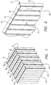
- the laminate structure 30 comprises a plurality of layers 10 (illustrated as layers 101 through 106) which are formed from initial sheets of acoustic attenuating material that are cut into an approximate shape.
- the material is an epoxy having acoustic absorbers and scatterers, such as tungsten, silica, chloroprene particles or air bubbles. While the material is not limited to epoxy, it must be both electrically insulating and acoustically absorbing.
- Each of the layers 10 has a front surface 12, a rear surface 14, a top surface 16 and a bottom surface 18.
- the front surface 12 is provided with an electrode coating 22.
- the exact thickness of the coating 22 can be selected to exhibit desired acoustic and structural qualities. If the coating 22 is too thick, it could adversely affect the acoustic properties of the material by increasing reflectivity of the rearward traveling acoustic wave. On the other hand, if the coating 22 is too thin, it could be of low conductivity or prone to discontinuities of conduction.
- the electrode coating 22 comprises a two metal coating having a first coating of chromium applied to a thickness of approximately 300 ⁇ ngströms, and a second coating of gold applied to a thickness of approximately 3000 ⁇ ngströms.
- the chromium promotes adhesion to the layer 10 and the gold provides a good quality electrical conductor which is resistant to oxidation.
- alternative materials could be used for the coating 22 as long as the desired electrical conductivity and material strength requirements are satisfied.
- the metal coatings can be applied by sputtering, plating, or other conventional techniques.
- the coated layer is patterned to provide a plurality of conductors 24, as shown in Figs. 1 and 2.
- Each conductor 24 extends between the top edge 16 and the bottom edge 18 of the layer 10, and is separated from adjacent conductors 24 by a gap 26.
- the patterning could be produced by a diamond saw, with the saw kerf forming the inter-conductor gap 26. The saw should cut into the layer 10 to a slight depth to further promote isolation of the individual conductors 24. Alternatively, the pattern could be produced by conventional photolithographic techniques.
- the individual conductors 24 are separated by a desired pitch, which is equivalent to the desired pitch of the piezoelectric elements of the transducer, as will be described below.
- the conductors 24 would have a pitch of 300 microns with a gap 26 spacing between each conductor of 50 microns.
- the particular spacing and pitch shown in the figures is for illustrative purposes only, and is not drawn to scale.
- the layers are combined together into the laminate structure 30 illustrated in Fig. 3.
- the layers 10 are combined under temperature and pressure with an electrically insulating epoxy or other adhesive which fills the gaps between the individual conductors.
- Each of the patterned layers 10 is oriented so that the conductors 24 extend between an upper surface 32 and a lower surface 34 of the laminate structure 30.
- the external surfaces are lapped with conventional machining processes to produce substantially flat and/or orthogonal surfaces. An edge portion 28 of each conductor 24 is exposed at the upper and lower lapped surfaces.
- a pattern of electrical contacts is provided on the lower surface 34 of the laminate structure 30.
- An electrode coating 38 is applied to the lower surface 34, in the same manner as the application of the coating 22 to the individual layers 10 described above.
- the bottom conductor 38 is then patterned to provide a plurality of individual conductive pads 46. Each pad 46 is electrically connected to an associated end of one of the conductors 24, as illustrated in phantom, and is patterned to match associated elements of the circuit element.
- the patterning can be produced by a conventional diamond saw, as substantially described above.
- the saw would first cut a plurality of vertical kerf lines 42 having dentical pitch as the gaps 26 between adjacent conductors 24 of the individual layers 10.
- the saw would then cut a plurality of horizonal kerf lines 44 spaced at midpoints of the individual layer 10 thicknesses.
- other patterning techniques such as photolithography can also be advantageously applied.
- a conductive coating 36 is applied in the same manner as that described above. However, prior to patterning the coating 36, a layer of piezoelectric material 48 is bonded onto the conductive coating.
- the piezoelectric material 48 may include any material which generates acoustic waves in response to an electric field applied across the material, such as but not limited to lead zirconium titanate.
- a low viscosity electrically insulating adhesive such as epoxy
- the adhesive is applied to a thickness of approximately one micron.
- the RMS roughness of the piezoelectric material 48 exceeds the bond thickness, so that when heat and pressure are applied the peaks of the piezoelectric material penetrate through the epoxy to form electrical connections between the piezoelectric material and the conductive coating 36.
- a matching layer 68 of graphite or polymer is applied onto the exposed surface of the piezoelectric material 48.
- the matching layer 68 increases the forward wave energy produced by the piezoelectric material 48, as known in the art.
- the combination of the piezoelectric material 48, the conductive coating 36 and the matching layer 68 is then patterned with vertical and horizontal kerf lines 42 and 44 in the same manner as that described above with respect to the bottom surface 34. It should be apparent that this technique permits self-alignment of the top conductive coating 36 to the vertical and horizonal kerf lines 42 and 44 with the laminate structure 30.
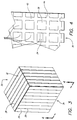
- the patterning technique results in a plurality of piezoelectric elements 52 disposed in a matrix each having an electrical conductor 24 extending through the acoustic attenuating backing material of the laminate structure 30 to an electrically conducting pad 46 disposed on a bottom surface 34 of the laminate structure.
- the pads 46 at the bottom surface 34 are substantially aligned to the piezoelectric elements 52 on the upper surface 32.
- a matrix of piezoelectric elements 52 of any desired dimension can be produced in this manner by simply increasing the size and number of the layers 10.
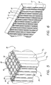
- each individual layer 10 has alternating electrical signal conductors 62 and ground conductors 64.
- the pitch of a combined pair of an electrical conductor 62 and a ground conductor 64 is equivalent to the pitch of a single electrical conductor 24 described above.
- the inclusion of interspersed ground conductors 64 is intended to reduce cross-talk of electrical signals between adjacent ones of the electrical signal conductors 62.
- the patterning of each layer 10 is performed using a diamond saw or a photolithographic process, as is substantially discussed above. However, at an upper edge of the layer 20, a ground path gap 66 is provided to prevent electrical connection between the ground conductor 64 and the piezoelectric element 52 which would be formed by the method discussed above.
- the patterning would match the spacing of the individual layer 10 so that distinct conductive pads 46 are produced for the electrical connection between the circuit element and the ground conductors 64 and the electrical conductors 62. It is intended that the ground conductors 64 be electrically connected to a ground potential, so that any cross-talk signal induced into the ground conductors would be shunted to ground.
- a second alternative embodiment is illustrated in Fig. 7.
- individual layers 10 would be divided in width through a first layer portion 72 and a second layer portion 74.
- a ground plane 76 is disposed between the first and second layer portions 72 and 74.
- the ground plane would similarly connect electrically to ground pads 46 disposed at the lower surface 34 of the assembled laminate structure 30, so as to shunt undesired cross-talk signals to ground.
- thermal conductors could be used in place of the ground planes 76 to eliminate excess heat from within the laminate structure 30. The thermal conductors would conduct excess heat within the structure 30 to an external heat sink (not shown).
- each electrical conductor 24 would dissipate low levels of electrical power, and thus would present a minimal thermal problem.
- the measured resistance for each individual conductor 24 is less than 1 ohm. Since the individual piezoelectric elements 52 have resistance of approximately 10,000 ohms and require approximately 100 volts for the transmit pulse, each conductor 24 can be expected to carry approximately 10 milliamps. Thus, each electrical conductor 24 could be expected to dissipate approximately 100 microwatts, which is relatively low.
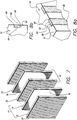
- Figs. 8a and 8b illustrate a third alternative embodiment of the invention.
- the individual layers 10 are patterned prior to applying the conductive coating 22 to form generally rectangular grooves 82.
- the rectangular grooves 82 are then coated with an electrically conductive coating including an electrically conductive backwall 84 and conductive sidewalls 86.
- the three-sided electrical conductor 80 is then filled with an electrically insulating epoxy 88, and the individual layers are combined as substantially described above into the single laminate structure 30.
- bottom conductive pads 46 are formed on the lower surface of the laminate structure 30, and individual piezoelectric elements 52 are disposed on an upper surface of the laminate structure.
- the three-sided conductor 80 would have a resistance roughly one-third of the conductor 24 described above.
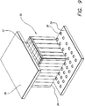
- Fig. 9 illustrates an exploded perspective view of an acoustic transducer 50 constructed in accordance with this invention.
- the transducer 50 attaches electrically to a circuit element illustrated as printed circuit board 54.
- the circuit element can also be a semiconductor, flexible cable or other device.
- the circuit board 54 has a plurality of electrical contact points 56 which match the position of the individual conductive pads 46 at the lower surface 34 of the transducer 50.
- a ground sheet 58 overlays the exposed upper portion of the individual piezoelectric elements 52 and electrically connects to the individual elements.
- the circuit board 54 provides electrical signals to the individual conductive pads 46 of the transducer 50.
- the electrical signals are conducted via the electrical conductors 24 through the layers 10 of the laminate structure 30 to the rearward surface of the individual piezoelectric elements 52.
- the acoustically transparent ground sheet 58 is disposed on the exposed surface of the transducer 50, and is placed in contact with the object of interest, such as the patient's skin. Utilization of the ground sheet 58 at the exposed surface of the piezoelectric elements 52 rather at the rearward surface prevents the patient from receiving an inadvertent electrical shock.
- the electrical signals which are inputted to the piezoelectric elements 52 are converted into acoustic wave energy which is transmitted through the ground sheet 58 into the subject.
- the wave energy transmitted from the transducer 50 is utilized to achieve echographic examination.
- the undesirable transmission of acoustic wave energy from the rearward faces of the piezoelectric elements 52 is absorbed by the laminate structure 30 formed from the acoustic absorbing material. Reflected wave energy received at the piezoelectric elements 52 is converted to an electrical signal that is conducted back through the electrical conductors 24 to the circuit board 54. This received signal would then be conditioned by known electrical circuitry on the circuit board.
- an array of any desired dimension can be produced by varying the number and size of the layers 10, and the pitch of the conductors 24 disposed on each layer.
Landscapes
- Engineering & Computer Science (AREA)
- Mechanical Engineering (AREA)
- Ultra Sonic Daignosis Equipment (AREA)
- Transducers For Ultrasonic Waves (AREA)
Applications Claiming Priority (2)
| Application Number | Priority Date | Filing Date | Title |
|---|---|---|---|
| US10300793A | 1993-08-05 | 1993-08-05 | |
| US103007 | 1993-08-05 |
Publications (2)
| Publication Number | Publication Date |
|---|---|
| EP0637470A2 true EP0637470A2 (de) | 1995-02-08 |
| EP0637470A3 EP0637470A3 (de) | 1995-11-22 |
Family
ID=22292863
Family Applications (1)
| Application Number | Title | Priority Date | Filing Date |
|---|---|---|---|
| EP94305729A Withdrawn EP0637470A3 (de) | 1993-08-05 | 1994-08-02 | Rückschicht für einen Anordnung von akustischen Wandler. |
Country Status (2)
| Country | Link |
|---|---|
| EP (1) | EP0637470A3 (de) |
| JP (1) | JPH0779498A (de) |
Cited By (11)
| Publication number | Priority date | Publication date | Assignee | Title |
|---|---|---|---|---|
| FR2740933A1 (fr) * | 1995-11-03 | 1997-05-09 | Thomson Csf | Sonde acoustique et procede de realisation |
| EP0727259A3 (de) * | 1995-02-15 | 1997-11-12 | Hewlett-Packard Company | Ultraschallwandler |
| EP0921757A4 (de) * | 1996-03-22 | 2000-03-15 | Lockheed Martin Ir Imaging Sys | Ultraschallanordnung mit dämpfende elektrische anschlüsse |
| WO2002040184A3 (en) * | 2000-11-15 | 2002-09-26 | Koninkl Philips Electronics Nv | Multidimensional ultrasonic transducer arrays |
| WO2005030055A1 (ja) | 2003-09-30 | 2005-04-07 | Matsushita Electric Industrial Co., Ltd. | 超音波探触子 |
| US7348713B2 (en) | 2004-10-05 | 2008-03-25 | Kabushiki Kaisha Toshiba | Ultrasonic probe |
| EP2623216A3 (de) * | 2012-01-31 | 2017-10-25 | Samsung Medison Co., Ltd. | Unterlagenelement einer Ultraschallsonde, Unterlagenschicht einer Ultraschallsonde und Herstellungsverfahren dafür |
| CN108461623A (zh) * | 2018-01-23 | 2018-08-28 | 长沙芬贝电子科技有限公司 | 一种用于阵列探头的背衬材料及其制造方法 |
| CN111050666A (zh) * | 2018-03-15 | 2020-04-21 | 株式会社日立制作所 | 超声波探头及其制造方法 |
| CN114938987A (zh) * | 2022-05-06 | 2022-08-26 | 苏州谱洛医疗科技有限公司 | 一种电连接板及超声换能装置 |
| EP4684886A1 (de) * | 2024-07-23 | 2026-01-28 | Siemens Medical Solutions USA, Inc. | Rückschicht mit integrierten masse- und signalleitern für einen ultraschallwandler |
Families Citing this family (3)
| Publication number | Priority date | Publication date | Assignee | Title |
|---|---|---|---|---|
| US7105986B2 (en) * | 2004-08-27 | 2006-09-12 | General Electric Company | Ultrasound transducer with enhanced thermal conductivity |
| JP2009153851A (ja) * | 2007-12-27 | 2009-07-16 | Konica Minolta Medical & Graphic Inc | 超音波診断装置およびそれに用いる配線の製造方法 |
| WO2010090095A1 (ja) | 2009-02-05 | 2010-08-12 | 株式会社林原生物化学研究所 | セロビオース2-エピメラーゼとその製造方法並びに用途 |
Family Cites Families (4)
| Publication number | Priority date | Publication date | Assignee | Title |
|---|---|---|---|---|
| DE3412665A1 (de) * | 1984-04-04 | 1985-10-17 | Siemens AG, 1000 Berlin und 8000 München | Vorrichtung zur auslese eines zweidimensionalen ladungsbildes mittels eines arrays |
| ATE63178T1 (de) * | 1986-08-11 | 1991-05-15 | Siemens Ag | Vorrichtung zum lesen eines zweidimensionalen ladungsbildes. |
| JP2545861B2 (ja) * | 1987-06-12 | 1996-10-23 | 富士通株式会社 | 超音波探触子の製造方法 |
| US5329498A (en) * | 1993-05-17 | 1994-07-12 | Hewlett-Packard Company | Signal conditioning and interconnection for an acoustic transducer |
-
1994
- 1994-08-02 EP EP94305729A patent/EP0637470A3/de not_active Withdrawn
- 1994-08-03 JP JP6201298A patent/JPH0779498A/ja active Pending
Cited By (19)
| Publication number | Priority date | Publication date | Assignee | Title |
|---|---|---|---|---|
| EP0727259A3 (de) * | 1995-02-15 | 1997-11-12 | Hewlett-Packard Company | Ultraschallwandler |
| FR2740933A1 (fr) * | 1995-11-03 | 1997-05-09 | Thomson Csf | Sonde acoustique et procede de realisation |
| WO1997017145A1 (fr) * | 1995-11-03 | 1997-05-15 | Thomson-Csf | Sonde acoustique et procede de realisation |
| EP0921757A4 (de) * | 1996-03-22 | 2000-03-15 | Lockheed Martin Ir Imaging Sys | Ultraschallanordnung mit dämpfende elektrische anschlüsse |
| WO2002040184A3 (en) * | 2000-11-15 | 2002-09-26 | Koninkl Philips Electronics Nv | Multidimensional ultrasonic transducer arrays |
| US7755255B2 (en) | 2003-09-30 | 2010-07-13 | Panasonic Corporation | Ultrasonic probe |
| CN100563577C (zh) * | 2003-09-30 | 2009-12-02 | 松下电器产业株式会社 | 超声波探头 |
| WO2005030055A1 (ja) | 2003-09-30 | 2005-04-07 | Matsushita Electric Industrial Co., Ltd. | 超音波探触子 |
| EP1671588A4 (de) * | 2003-09-30 | 2013-08-07 | Panasonic Corp | Ultraschallsonde |
| CN1897876B (zh) * | 2004-10-05 | 2011-03-02 | 株式会社东芝 | 超声探头 |
| US7348713B2 (en) | 2004-10-05 | 2008-03-25 | Kabushiki Kaisha Toshiba | Ultrasonic probe |
| US10390793B2 (en) | 2012-01-31 | 2019-08-27 | Samsung Medison Co., Ltd. | Backing element of ultrasonic probe, backing layer of ultrasonic probe, and manufacturing method thereof |
| EP2623216A3 (de) * | 2012-01-31 | 2017-10-25 | Samsung Medison Co., Ltd. | Unterlagenelement einer Ultraschallsonde, Unterlagenschicht einer Ultraschallsonde und Herstellungsverfahren dafür |
| CN108461623A (zh) * | 2018-01-23 | 2018-08-28 | 长沙芬贝电子科技有限公司 | 一种用于阵列探头的背衬材料及其制造方法 |
| CN108461623B (zh) * | 2018-01-23 | 2024-05-14 | 曼图电子(上海)有限公司 | 一种用于阵列探头的背衬材料及其制造方法 |
| CN111050666A (zh) * | 2018-03-15 | 2020-04-21 | 株式会社日立制作所 | 超声波探头及其制造方法 |
| CN111050666B (zh) * | 2018-03-15 | 2022-05-27 | 富士胶片医疗健康株式会社 | 超声波探头及其制造方法 |
| CN114938987A (zh) * | 2022-05-06 | 2022-08-26 | 苏州谱洛医疗科技有限公司 | 一种电连接板及超声换能装置 |
| EP4684886A1 (de) * | 2024-07-23 | 2026-01-28 | Siemens Medical Solutions USA, Inc. | Rückschicht mit integrierten masse- und signalleitern für einen ultraschallwandler |
Also Published As
| Publication number | Publication date |
|---|---|
| EP0637470A3 (de) | 1995-11-22 |
| JPH0779498A (ja) | 1995-03-20 |
Similar Documents
| Publication | Publication Date | Title |
|---|---|---|
| US6936008B2 (en) | Ultrasound system with cableless coupling assembly | |
| US5559388A (en) | High density interconnect for an ultrasonic phased array and method for making | |
| US5792058A (en) | Broadband phased array transducer with wide bandwidth, high sensitivity and reduced cross-talk and method for manufacture thereof | |
| US5644085A (en) | High density integrated ultrasonic phased array transducer and a method for making | |
| US5329498A (en) | Signal conditioning and interconnection for an acoustic transducer | |
| JP3279375B2 (ja) | 音響変換器アレイのための支持体 | |
| US5629906A (en) | Ultrasonic transducer | |
| US6625856B2 (en) | Method of manufacturing an ultrasonic transducer | |
| EP1436097B1 (de) | Verfahren zum kontaktieren eines akustischen elementes an eine integrierte schaltung | |
| EP0637470A2 (de) | Rückschicht für einen Anordnung von akustischen Wandler | |
| US5655538A (en) | Ultrasonic phased array transducer with an ultralow impedance backfill and a method for making | |
| EP0128049B1 (de) | Ultraschallsende mit einem absorbierenden Träger | |
| US5894646A (en) | Method for the manufacture of a two dimensional acoustic array | |
| US5545942A (en) | Method and apparatus for dissipating heat from a transducer element array of an ultrasound probe | |
| US7834522B2 (en) | Diagnostic ultrasound transducer | |
| US20030018267A1 (en) | Piezocomposite ultrasound array and integrated circuit assembly with improved thermal expansion and acoustical crosstalk characteristics | |
| EP0294826A1 (de) | Ultraschallwandlerstruktur | |
| EP0206432A1 (de) | Phasengesteuerte Wandleranordnung für medizinische Ultraschallabbildung | |
| KR101031010B1 (ko) | 피씨비 및 이를 구비하는 프로브 | |
| CN1890707B (zh) | 实施装有ic并带有高衰减背载的传感器 | |
| EP0120657B1 (de) | Zweifach anwendbare Ultraschallwandleranordnung | |
| US5275167A (en) | Acoustic transducer with tab connector | |
| JP3033480B2 (ja) | 超音波探触子 | |
| JPH05123317A (ja) | 2次元アレイ超音波プローブ | |
| JP3934202B2 (ja) | 超音波探触子 |
Legal Events
| Date | Code | Title | Description |
|---|---|---|---|
| PUAI | Public reference made under article 153(3) epc to a published international application that has entered the european phase |
Free format text: ORIGINAL CODE: 0009012 |
|
| AK | Designated contracting states |
Kind code of ref document: A2 Designated state(s): DE FR GB NL |
|
| PUAL | Search report despatched |
Free format text: ORIGINAL CODE: 0009013 |
|
| AK | Designated contracting states |
Kind code of ref document: A3 Designated state(s): DE FR GB NL |
|
| STAA | Information on the status of an ep patent application or granted ep patent |
Free format text: STATUS: THE APPLICATION IS DEEMED TO BE WITHDRAWN |
|
| 18D | Application deemed to be withdrawn |
Effective date: 19960523 |