EP0637876A1 - Boucle à synchronisation de phase et méthode de fonctionnement - Google Patents
Boucle à synchronisation de phase et méthode de fonctionnement Download PDFInfo
- Publication number
- EP0637876A1 EP0637876A1 EP94110942A EP94110942A EP0637876A1 EP 0637876 A1 EP0637876 A1 EP 0637876A1 EP 94110942 A EP94110942 A EP 94110942A EP 94110942 A EP94110942 A EP 94110942A EP 0637876 A1 EP0637876 A1 EP 0637876A1
- Authority
- EP
- European Patent Office
- Prior art keywords
- frequency
- clock signal
- circuit
- divide
- output
- Prior art date
- Legal status (The legal status is an assumption and is not a legal conclusion. Google has not performed a legal analysis and makes no representation as to the accuracy of the status listed.)
- Withdrawn
Links
- 238000000034 method Methods 0.000 title claims description 8
- 238000004519 manufacturing process Methods 0.000 description 8
- 230000007423 decrease Effects 0.000 description 7
- 230000004048 modification Effects 0.000 description 5
- 238000012986 modification Methods 0.000 description 5
- 238000010586 diagram Methods 0.000 description 4
- 230000010355 oscillation Effects 0.000 description 4
- 230000003247 decreasing effect Effects 0.000 description 3
- 239000003990 capacitor Substances 0.000 description 2
- 230000008859 change Effects 0.000 description 2
- 230000000737 periodic effect Effects 0.000 description 2
- 238000012358 sourcing Methods 0.000 description 2
- 230000000704 physical effect Effects 0.000 description 1
- 230000008569 process Effects 0.000 description 1
- 230000009467 reduction Effects 0.000 description 1
- 230000004044 response Effects 0.000 description 1
- 230000035945 sensitivity Effects 0.000 description 1
Images
Classifications
-
- H—ELECTRICITY
- H03—ELECTRONIC CIRCUITRY
- H03L—AUTOMATIC CONTROL, STARTING, SYNCHRONISATION OR STABILISATION OF GENERATORS OF ELECTRONIC OSCILLATIONS OR PULSES
- H03L7/00—Automatic control of frequency or phase; Synchronisation
- H03L7/06—Automatic control of frequency or phase; Synchronisation using a reference signal applied to a frequency- or phase-locked loop
- H03L7/16—Indirect frequency synthesis, i.e. generating a desired one of a number of predetermined frequencies using a frequency- or phase-locked loop
- H03L7/18—Indirect frequency synthesis, i.e. generating a desired one of a number of predetermined frequencies using a frequency- or phase-locked loop using a frequency divider or counter in the loop
- H03L7/183—Indirect frequency synthesis, i.e. generating a desired one of a number of predetermined frequencies using a frequency- or phase-locked loop using a frequency divider or counter in the loop a time difference being used for locking the loop, the counter counting between fixed numbers or the frequency divider dividing by a fixed number
-
- H—ELECTRICITY
- H03—ELECTRONIC CIRCUITRY
- H03L—AUTOMATIC CONTROL, STARTING, SYNCHRONISATION OR STABILISATION OF GENERATORS OF ELECTRONIC OSCILLATIONS OR PULSES
- H03L7/00—Automatic control of frequency or phase; Synchronisation
-
- H—ELECTRICITY
- H03—ELECTRONIC CIRCUITRY
- H03L—AUTOMATIC CONTROL, STARTING, SYNCHRONISATION OR STABILISATION OF GENERATORS OF ELECTRONIC OSCILLATIONS OR PULSES
- H03L7/00—Automatic control of frequency or phase; Synchronisation
- H03L7/06—Automatic control of frequency or phase; Synchronisation using a reference signal applied to a frequency- or phase-locked loop
- H03L7/08—Details of the phase-locked loop
- H03L7/085—Details of the phase-locked loop concerning mainly the frequency- or phase-detection arrangement including the filtering or amplification of its output signal
- H03L7/087—Details of the phase-locked loop concerning mainly the frequency- or phase-detection arrangement including the filtering or amplification of its output signal using at least two phase detectors or a frequency and phase detector in the loop
-
- H—ELECTRICITY
- H03—ELECTRONIC CIRCUITRY
- H03L—AUTOMATIC CONTROL, STARTING, SYNCHRONISATION OR STABILISATION OF GENERATORS OF ELECTRONIC OSCILLATIONS OR PULSES
- H03L7/00—Automatic control of frequency or phase; Synchronisation
- H03L7/06—Automatic control of frequency or phase; Synchronisation using a reference signal applied to a frequency- or phase-locked loop
- H03L7/08—Details of the phase-locked loop
- H03L7/085—Details of the phase-locked loop concerning mainly the frequency- or phase-detection arrangement including the filtering or amplification of its output signal
- H03L7/089—Details of the phase-locked loop concerning mainly the frequency- or phase-detection arrangement including the filtering or amplification of its output signal the phase or frequency detector generating up-down pulses
- H03L7/0891—Details of the phase-locked loop concerning mainly the frequency- or phase-detection arrangement including the filtering or amplification of its output signal the phase or frequency detector generating up-down pulses the up-down pulses controlling source and sink current generators, e.g. a charge pump
- H03L7/0895—Details of the current generators
- H03L7/0898—Details of the current generators the source or sink current values being variable
Definitions
- the present invention generally relates to phase locked loops, and more specifically to a phase locked loop with improved frequency bandwidth.
- Phase locked loops are a class of devices that match the phase and frequency of a reference clock signal with the phase and frequency of an output clock signal. PLLs are widely used in frequency modulation (FM) radio and digital computing applications.
- FM frequency modulation
- Some PLLs generate an output clock signal with a frequency which is some multiple of the reference clock signal frequency.
- This modification may be advantageous in radio applications in which the radio transmits and receives at some multiple of a commonly available reference clock signal.
- This modification may also be advantageous to data processing systems in which the data processor operates at some multiple of an input reference clock signal, such as a bus clock signal.
- Divide-by-P circuits (where P is an integer) can be used to generate the frequency modification described above.
- a divide-by-P circuit can be interposed between the reference clock signal and the PLL's input to generate an output clock signal that is (1/P) times as slow as the reference clock signal.
- a divide-by-M circuit (where M is an integer) can be interposed in the feedback loop of the output clock signal to generate an output clock signal that is (M) times as fast as the reference clock signal.
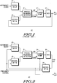
- FIG. 1 depicts a block diagram of a phase locked loop 10 known in the art.
- PLL 10 has a phase/frequency detector 12, a charge pump 14, a voltage controlled oscillator (hereafter simply "VCO") 16, a divide-by-M circuit 18 and a divide-by-P circuit 20, where M and P are integers.
- VCO voltage controlled oscillator
- PLL 10 generates an output clock signal, PLL OUT, that has a predetermined phase and frequency relationship to an input signal REFERENCE CLOCK.
- PLL 10 dynamically adjusts the phase and frequency of the output clock signal PLL OUT to match the phase and frequency of the reference clock signal.
- Phase/frequency detector 12 receives the two clock signals and generates UP and DOWN control signals. If the clock signal output by divide-by-M circuit 18 has a lower frequency than the clock signal output by divide-by-P circuit 20, then phase/frequency detector 12 asserts the UP signal. Conversely, if the clock signal output by divide-by-M circuit 18 has a higher frequency than the clock signal output by divide-by-P circuit 20, then phase/frequency detector 12 asserts the DOWN signal. When the two clock signals have substantially the same phase and frequency, then phase/frequency detector 12 asserts neither signal.
- Charge pump 10 charges or discharges a node (not shown) responsive to the output signals UP and DOWN of phase/frequency detector 14. Typically, the node is connected to ground through a resistor and a capacitor connected in series. Charge pump 10 charges the node when the UP control signal is asserted by sourcing an electrical current to the node. Charge pump 10 discharges the node when the DOWN control signal is asserted by sinking an electrical current from the node.
- VCO 16 generates a periodic clock signal (labeled PLL OUT) responsive to the voltage present on the node of charge pump 14.
- VCO 16 may have within it a ring oscillator connected to a first and a second power rail through a first and a second transistor, respectively.
- an increase in the voltage present on output node 12 causes the conductivity of the first or second transistors to increase, thereby increasing the oscillation frequency of the ring oscillator.
- a decrease in the voltage present on output node 12 causes the conductivity of the first or second transistors to decrease, thereby decreasing the oscillation frequency of the ring oscillator.
- VCO 16 generates the output of PLL 22 (labeled PLL OUT).
- Divide-By-M circuit 18 receives the signal PLL OUT and reduces the frequency of the signal by an integer ratio M.
- Divide-By-P circuit 20 receives the signal REFERENCE CLOCK and reduces the frequency of the signal by an integer ratio P.
- the output of divide-by-M circuit 18 and divide-By-P circuit 20 are input to phase/frequency detector 12. It is these two signals which phase/frequency detector 12 aligns.
- PLL 10 may generate an output clock signal that has a frequency different from the reference clock signal with the addition of divide-by-M circuit 18 or divide-by-P circuit 20.
- the frequency of a PLL's output clock signal may be varied by inserting a programmable divide-by-M circuit or programmable divide-by-P circuit in the appropriate location.
- a PLL incorporating such a divider may generate a clock signal with different frequencies depending upon the settings of the inserted divider circuit. This flexibility may be required or may be simply desirable depending upon the application. For instance, in many FM radio systems, the associated PLL must be able to generate different output clock frequencies for different operating frequencies. In data processing systems, it may be desirable to generate an output clock signal with the maximum permissible frequency allowed by the data processor independent of the input clock signal.
- a programmable PLL allows a data processor to operate at its maximum clock speed in a wide variety of circumstances. In this latter case, the setting of the divide-by circuits may be adjusted to increase the ratio (M/P) as the frequency of the input clock signal decreases.
- the operating characteristics of the VCO are typically the limiting constraints of a PLL.
- the bandwidth of the VCO is limited by the maximum frequency of the worst case manufacturing result and the minimum frequency of the best case manufacturing result. The difference of these two frequencies is the bandwidth of the VCO for the particular manufacturing process. Therefore, a designer trying to increase the bandwidth of a PLL has two design choices: (1) he can modify or "tweak" his manufacturing process to improve circuit performance; or (2) he can use a divide-by-M circuit and increase the value of M. Tweaking manufacturing processes is an expensive solution. Further, the results of a process tweak are difficult to predict. The use of a divide-by-M circuit can increase the effective bandwidth of a PLL.
- phase locked loop having a combination of divide-by circuits which substantially eliminates disadvantages of phase locked loops.
- a phase locked loop that generates an output clock signal has a phase/frequency circuit, a charge pump circuit, a voltage controlled oscillator circuit, a first divide-by circuit and a second divide-by circuit.
- the phase/frequency circuit generates a first control signal responsive to a predetermined phase relationship between a first and a second clock signal.
- the charge pump circuit generates a voltage responsive to the first control signal.
- the voltage controlled oscillator circuit generates a third clock signal responsive to the voltage.
- the first and second divide-by circuits serially reduce the frequency of the third clock cycle by a first and a second ratio, respectively. The first ratio is controlled by a second control signal.
- the output of the first divide-by circuit generates the output clock signal.
- the output of the second divide-by circuit generates the first clock signal.
- a method of generating an output clock signal comprises the steps of receiving a first clock signal and a second clock signal at a phase/frequency circuit and generating a first control signal responsive to a predetermined phase relationship between the first and second clock signals.
- the method also has the steps of generating a voltage by a charge pump circuit responsive to the first control signal and generating a third clock signal by a voltage controlled oscillator responsive to the voltage.
- the method has the steps of generating an output clock signal by a first divide-by circuit and generating the first clock signal by a second divide-by circuit.
- the ratio of the frequency of the output clock signal and the frequency of the third clock signal are responsive to a second control signal.
- the ratio of the frequency of the first clock signal and the frequency of the output clock signal are a predetermined ratio.
- FIG. 2 depicts a block diagram of a phase locked loop 22 constructed in accordance with the present invention.
- PLL 22 has a phase/frequency detector 12, a charge pump 14, a voltage controlled oscillator (hereafter simply "VCO") 16, a divide-by-M circuit 18, a divide-by-P circuit 20 and a divide-by-N circuit 24, where M, N and P are positive real numbers.
- VCO voltage controlled oscillator
- the combination of divide-by circuits 18 and 24 in the PLL feedback loop increases the difference between highest and lowest input frequency for a given VCO bandwidth, increases the number of possible ratios between input and output frequency and reduces re-lock time. Consequently, a manufacturing process that ordinarily yields a VCO with a narrow bandwidth may be used to manufacture a PLL with a much larger input frequency range.
- PLL 22 generates an output clock signal, PLL OUT, that has a predetermined phase and frequency relationship to an input signal REFERENCE CLOCK.
- PLL 22 dynamically adjusts the phase and frequency of the output clock signal to match the phase and frequency of the reference clock signal or adjusts the phase and frequency of the output clock signal to match the phase and frequency of a multiple of the reference clock signal.
- Phase/frequency detector 12 receives the two clock signals and generates UP and DOWN control signals. If the clock signal output by divide-by-M circuit 18 has a lower frequency than the clock signal output by divide-by-P circuit 20, then phase/frequency detector 12 asserts the UP signal (or a predetermined edge of the clock signal output by divide-by-M circuit 18 lags the same edge of the clock signal output by divide-by-P circuit 20). Conversely, if the clock signal output by divide-by-M circuit 18 has a higher frequency than the clock signal output by divide-by-P circuit 20, then phase/frequency detector 12 asserts the DOWN signal (or a predetermined edge of the clock signal output by divide-by-M circuit 18 leads the same edge of the clock signal output by divide-by-P circuit 20). When the two clock signals have substantially the same phase and frequency, then phase/frequency detector 12 asserts neither signal.
- Charge pump 10 charges or discharges a node (not shown) responsive to the output signals UP and DOWN of phase/frequency detector 14.
- the node is connected to ground through a resistor and a capacitor connected in series.
- Charge pump 10 charges the node when the UP control signal is asserted by sourcing an electrical current to the node.
- Charge pump 10 discharges the node when the DOWN control signal is asserted by sinking an electrical current from the node.
- One embodiment of the disclosed invention incorporates a charge pump 10 that has a programmable pump current.
- the pump current is the current that charges or discharges the node described above.
- a variable current allows charge pump 10 to behave consistently over a range of divide-by circuit settings.
- charge-pump 10 receives a control signal labeled FREQUENCY CONTROL.
- FREQUENCY CONTROL a control signal labeled FREQUENCY CONTROL.
- VCO 16 generates a periodic clock signal, VCO OUT, responsive to the voltage present on the node of charge pump 14.
- VCO 16 may have within it a ring oscillator connected to a first and a second power rail through a first and a second transistor, respectively.
- an increase in the voltage present on output node 12 causes the conductivity of the first or second transistors to increase, thereby increasing the oscillation frequency of the ring oscillator.
- a decrease in the voltage present on output node 12 causes the conductivity of the first or second transistors to decrease, thereby decreasing the oscillation frequency of the ring oscillator.
- Divide-By-N circuit 24 receives the signal VCO OUT and reduces the frequency of the signal by a ratio N.
- the output of divide-by-N circuit 22 generates the output of PLL 22 (labeled PLL OUT).
- Divide-By-M circuit 18 receives the signal PLL OUT and further reduces the frequency of the signal VCO OUT by a ratio M.
- Divide-By-P circuit 20 receives the signal REFERENCE CLOCK and reduces the frequency of the signal by a ratio P.
- the output of divide-by-M circuit 18 and divide-By-P circuit 20 are input to phase/frequency detector 12. It is these two signals which phase/frequency detector 12 aligns.
- PLL 22 can generate an output clock signal that has a frequency different from the reference clock signal with the addition of divide-by-M circuit 18 or divide-by-P circuit 20.
- divide-by-M circuit 18 and divide-by-P circuit 20 receive a control signal labeled FREQUENCY CONTROL. It should be understood that the control signal FREQUENCY CONTROL may contain several signals or sets of signals.
- the control signal FREQUENCY CONTROL selects the divisor of divide-by-M circuit 18 and divide-by-P circuit 20.
- Divide-by-M circuit 18 and divide-by-P circuit 20 are individually programmable. Therefore, PLL 22 may generate a clock signal with different frequencies depending upon the settings of the inserted divider circuits.
- the frequency of the output of VCO 16 (labeled VCO OUT) is not necessarily equal to the frequency of the output signal (labeled PLL OUT).
- the control signal FREQUENCY CONTROL also selects the divisor of divide-by-N circuit 24.
- PLL 22 is programmed to generate a signal having a frequency equal to some predetermined ratio times the frequency of the reference signal. (For purposes of simplifying the following explanation, P is assumed to equal one.) Therefore, it is the PLL's function to match the frequency and phase of the reference signal, generally a constant frequency signal.
- PLL 22 is programmed to generate an output signal having a frequency equal to some varying ratio times the frequency of the reference signal.
- the reference signal may be assumed to have a generally constant frequency. Therefore, it is the PLL's function to change the frequency of the output signal, typically in large increments.
- the above described functional bifurcation is arbitrary and for purposes of illustrating the disclosed PLL. In a real application, the disclosed invention could be used to both match a generally constant frequency reference signal and vary the ratio of the frequencies of the input and output signals.
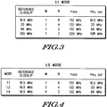
- FIG. 3 depicts in tabular form four configurations of PLL 22 illustrated in FIG. 2.
- FIG. 2 depicts a first mode of operation of PLL 22.
- PLL 22 is required to output a clock signal that matches some predetermined ratio of the input reference signal.
- the ratio is 1:1.
- the frequency of the input signal differs.
- the frequency of the reference signal might vary if the signal itself varied or if PLL 22 was designed to operate in an environment where the reference clock could have any one of several values.
- the frequency of the input clock signal varies from 16.5 MHz to 100 MHz.
- the ratio (M/P) determines the ratio of the output clock signal and the input clock signal.
- the frequency of VCO 16 may be modified independent of the output frequency by varying N.
- the frequency of the VCO OUT signal may be maintained at 132 MHz in the first through third configurations by varying N from eight to four to two.
- the frequency of the VCO OUT signal increases to 200 MHz in the fourth configuration.
- the required bandwidth of a VCO in a particular application is the difference between the maximum and minimum VCO frequency required in the application.
- the bandwidth of the VCO is 68 MHz (200 MHz - 132 MHz).
- the bandwidth of a known VCO designed to operate in four configurations similar to those depicted in TABLE 1 is 167 MHz.
- Such a known PLL has a divide-by-M circuit with M equal to two (to insure a 50% duty cycle) and no divide-by-N circuit.
- the VCO in this known PLL would operate at 33 and 200 MHz in the first and fourth configurations, respectively.
- the disclosed PLL significantly increases the capabilities of a given VCO or conversely, eases the manufacturing process and the physical property limitations for a given circuit specification.
- FIG. 4 depicts in tabular form three configurations of PLL 22 illustrated in FIG. 2.
- FIG. 2 depicts a second mode of operation of PLL 22.
- PLL 22 is required to output a clock signal that matches a particular ratio of the input reference signal.
- the particular ratio varies in each configuration.
- the input signal input frequency remains constant.
- the ratio of frequencies might vary if, for instance, PLL 22 was part of a data processor designed to operate in an environment in which the data processor and its bus operated at different frequencies.
- the frequency ratios are 1:1, 1:2, and 1:4 and the input clock signals is a constant 16.5 MHz.
- the ratio (M/P) determines the ratio of the output clock signal and the input clock signal.
- the value of N may be varied so that the product (N*M) is constant.
- the product (N*M) is a constant value of eight value.
- This mode of operation maintains a constant VCO frequency of 132 MHz.
- a circuit incorporating PLL 22 may switch between these three configurations without changing the frequency of VCO 14. This operating strategy is known as "switching on the fly.”
- Divide-by-N circuit 24 allows PLL 22 to relock input and output clock signals after a ratio change with little or no delay.
- divide-by-P circuit 20 is not necessary to practice the disclosed invention.
- the particular range of frequency reductions that divide-by-M circuit 18 and divide-by-N circuit 24 are each capable of is implementation specific. It is to be understood therefore, that the invention encompasses all such modifications that do not depart from the spirit and scope of the invention as defined in the appended claims.
Landscapes
- Stabilization Of Oscillater, Synchronisation, Frequency Synthesizers (AREA)
Applications Claiming Priority (2)
| Application Number | Priority Date | Filing Date | Title |
|---|---|---|---|
| US10095193A | 1993-08-03 | 1993-08-03 | |
| US100951 | 1993-08-03 |
Publications (1)
| Publication Number | Publication Date |
|---|---|
| EP0637876A1 true EP0637876A1 (fr) | 1995-02-08 |
Family
ID=22282372
Family Applications (1)
| Application Number | Title | Priority Date | Filing Date |
|---|---|---|---|
| EP94110942A Withdrawn EP0637876A1 (fr) | 1993-08-03 | 1994-07-14 | Boucle à synchronisation de phase et méthode de fonctionnement |
Country Status (4)
| Country | Link |
|---|---|
| EP (1) | EP0637876A1 (fr) |
| JP (1) | JPH07154246A (fr) |
| KR (1) | KR950007297A (fr) |
| TW (1) | TW236052B (fr) |
Cited By (5)
| Publication number | Priority date | Publication date | Assignee | Title |
|---|---|---|---|---|
| WO1996007240A1 (fr) * | 1994-08-31 | 1996-03-07 | Polaroid Corporation | Boucle compensee a phase asservie servant a generer un signal d'horloge de sortie regulee |
| WO1998034338A1 (fr) * | 1997-02-05 | 1998-08-06 | Fox Enterprises, Inc. | Oscillateur a quartz programmable |
| US5960405A (en) * | 1997-02-05 | 1999-09-28 | Fox Enterprises, Inc. | Worldwide marketing logistics network including strategically located centers for frequency programming crystal oscillators to customer specification |
| US6718473B1 (en) * | 2000-09-26 | 2004-04-06 | Sun Microsystems, Inc. | Method and apparatus for reducing power consumption |
| EP2164175A1 (fr) * | 2008-09-11 | 2010-03-17 | Sicon Semiconductor AB | Boucle à verrouillage de phase |
Citations (1)
| Publication number | Priority date | Publication date | Assignee | Title |
|---|---|---|---|---|
| EP0072271A1 (fr) * | 1981-07-24 | 1983-02-16 | Thomson-Csf | Synthétiseur de fréquence à large bande relative |
-
1993
- 1993-10-15 TW TW082108651A patent/TW236052B/zh active
-
1994
- 1994-07-14 EP EP94110942A patent/EP0637876A1/fr not_active Withdrawn
- 1994-07-27 JP JP6193885A patent/JPH07154246A/ja active Pending
- 1994-07-29 KR KR1019940018563A patent/KR950007297A/ko not_active Withdrawn
Patent Citations (1)
| Publication number | Priority date | Publication date | Assignee | Title |
|---|---|---|---|---|
| EP0072271A1 (fr) * | 1981-07-24 | 1983-02-16 | Thomson-Csf | Synthétiseur de fréquence à large bande relative |
Non-Patent Citations (1)
| Title |
|---|
| RICHARD YEAGER: "Loop Gain Compensation in Phase-Locked Loops", RCA REVIEW, vol. 47, March 1986 (1986-03-01), PRINCETON US, pages 78 - 87 * |
Cited By (12)
| Publication number | Priority date | Publication date | Assignee | Title |
|---|---|---|---|---|
| WO1996007240A1 (fr) * | 1994-08-31 | 1996-03-07 | Polaroid Corporation | Boucle compensee a phase asservie servant a generer un signal d'horloge de sortie regulee |
| WO1998034338A1 (fr) * | 1997-02-05 | 1998-08-06 | Fox Enterprises, Inc. | Oscillateur a quartz programmable |
| US5952890A (en) * | 1997-02-05 | 1999-09-14 | Fox Enterprises, Inc. | Crystal oscillator programmable with frequency-defining parameters |
| US5960405A (en) * | 1997-02-05 | 1999-09-28 | Fox Enterprises, Inc. | Worldwide marketing logistics network including strategically located centers for frequency programming crystal oscillators to customer specification |
| US6188290B1 (en) | 1997-02-05 | 2001-02-13 | Fox Enterprises, Inc. | Method of initializing an oscillator circuit |
| US6664860B2 (en) | 1997-02-05 | 2003-12-16 | Fox Enterprises, Inc. | Programmable oscillator circuit and method |
| US6954113B2 (en) | 1997-02-05 | 2005-10-11 | Fox Electronics, Inc. | Programmable oscillator circuit |
| US6965272B2 (en) | 1997-02-05 | 2005-11-15 | Fox Enterprises, Inc. | Worldwide marketing logistics network including strategically located centers for frequency programming crystal oscillators to customer specification |
| US6718473B1 (en) * | 2000-09-26 | 2004-04-06 | Sun Microsystems, Inc. | Method and apparatus for reducing power consumption |
| EP2164175A1 (fr) * | 2008-09-11 | 2010-03-17 | Sicon Semiconductor AB | Boucle à verrouillage de phase |
| WO2010029114A1 (fr) * | 2008-09-11 | 2010-03-18 | Zoran Corporation | Boucle à verrouillage de phase |
| US8576970B2 (en) | 2008-09-11 | 2013-11-05 | Csr Technology Inc. | Phase-locked loop |
Also Published As
| Publication number | Publication date |
|---|---|
| KR950007297A (ko) | 1995-03-21 |
| JPH07154246A (ja) | 1995-06-16 |
| TW236052B (en) | 1994-12-11 |
Similar Documents
| Publication | Publication Date | Title |
|---|---|---|
| US5610955A (en) | Circuit for generating a spread spectrum clock | |
| US6181213B1 (en) | Phase-locked loop having a multi-phase voltage controlled oscillator | |
| US5648744A (en) | System and method for voltage controlled oscillator automatic band selection | |
| JP3098027B2 (ja) | 位相ロック回路及び該位相ロック回路より成る周波数逓倍器 | |
| US6229399B1 (en) | Multiple frequency band synthesizer using a single voltage control oscillator | |
| US6147561A (en) | Phase/frequency detector with time-delayed inputs in a charge pump based phase locked loop and a method for enhancing the phase locked loop gain | |
| US5420545A (en) | Phase lock loop with selectable frequency switching time | |
| JP2710214B2 (ja) | フェーズロックドループ回路 | |
| US5703540A (en) | Voltage-controlled crystal oscillator with extended range | |
| US9160353B2 (en) | Phase frequency detector and charge pump for phase lock loop fast-locking | |
| CN1195432A (zh) | 频率合成器中用于控制压控振荡器调谐范围的方法与装置 | |
| JPH10242856A (ja) | 可変速度位相ロック・ループ・システムおよびその方法 | |
| US7352837B2 (en) | Digital phase-locked loop | |
| US7356111B1 (en) | Apparatus and method for fractional frequency division using multi-phase output VCO | |
| US6661291B2 (en) | Fractional and rapid response frequency synthesizer, and corresponding frequency synthesizing method | |
| EP0755120A1 (fr) | Circuit de boucle à verrouillage de phase | |
| US6693987B1 (en) | Digital-to-analog DAC-driven phase-locked loop PLL with slave PLL's driving DAC reference voltages | |
| US6281727B1 (en) | Fine-tuning phase-locked loop PLL using variable resistor between dual PLL loops | |
| US7332945B2 (en) | Divider having dual modulus pre-scaler and an associated method | |
| JP2842847B2 (ja) | Pllシンセサイザ回路 | |
| JPH07154246A (ja) | 位相同期ループおよび動作方法 | |
| US20030214330A1 (en) | Phase-locked loop circuit | |
| US7659785B2 (en) | Voltage controlled oscillator and PLL having the same | |
| US7834666B2 (en) | Voltage divider having varied output levels depending on frequency and PLL including the same | |
| US7388440B1 (en) | Circuit and method to speed up PLL lock-time and prohibit frequency runaway |
Legal Events
| Date | Code | Title | Description |
|---|---|---|---|
| PUAI | Public reference made under article 153(3) epc to a published international application that has entered the european phase |
Free format text: ORIGINAL CODE: 0009012 |
|
| AK | Designated contracting states |
Kind code of ref document: A1 Designated state(s): DE FR GB IE IT |
|
| STAA | Information on the status of an ep patent application or granted ep patent |
Free format text: STATUS: THE APPLICATION IS DEEMED TO BE WITHDRAWN |
|
| 18D | Application deemed to be withdrawn |
Effective date: 19950809 |