EP0638825A2 - Verfahren zur Erkennung von ionisierender Strahlung - Google Patents
Verfahren zur Erkennung von ionisierender Strahlung Download PDFInfo
- Publication number
- EP0638825A2 EP0638825A2 EP94305975A EP94305975A EP0638825A2 EP 0638825 A2 EP0638825 A2 EP 0638825A2 EP 94305975 A EP94305975 A EP 94305975A EP 94305975 A EP94305975 A EP 94305975A EP 0638825 A2 EP0638825 A2 EP 0638825A2
- Authority
- EP
- European Patent Office
- Prior art keywords
- diamond
- ions
- diamond body
- ppm
- range
- Prior art date
- Legal status (The legal status is an assumption and is not a legal conclusion. Google has not performed a legal analysis and makes no representation as to the accuracy of the status listed.)
- Granted
Links
Images
Classifications
-
- G—PHYSICS
- G01—MEASURING; TESTING
- G01T—MEASUREMENT OF NUCLEAR OR X-RADIATION
- G01T1/00—Measuring X-radiation, gamma radiation, corpuscular radiation, or cosmic radiation
- G01T1/16—Measuring radiation intensity
- G01T1/26—Measuring radiation intensity with resistance detectors
Definitions
- THIS invention relates to a method of manufacturing a sensor for detecting ionising radiation and to a diamond sensor element formed by the method.
- a method of manufacturing a radiation sensor element comprises the steps of: providing a diamond body comprising crystalline diamond material having a nitrogen impurity concentration as determined by ESR techniques of 150 ppm or less; and hydrogenating the body to cause atomic hydrogen to be incorporated into the diamond crystal lattice.
- the diamond material preferably has a nitrogen impurity concentration of 60 ppm or less, and most preferably less than 10 ppm.
- the diamond body will typically be selected as having the properties of a counting diamond or a diamond which is capable of exhibiting thermoluminescence when subjected to ionising radiation.
- the diamond body may comprise a synthetic diamond manufactured by a high temperature/high pressure process, or by a chemical vapour deposition (CVD) process.
- CVD chemical vapour deposition
- the diamond body is a single crystal diamond.
- the diamond body may be hydrogenated by means of an ion implantation process.
- the ions may be implanted with an energy in the range 1 keV to 1 MeV, preferably 35 keV to 170 keV, and with an ion dose in the range 1016 ions/cm2 to 1018 ions/cm2.
- the diamond body is preferably maintained at a temperature in the range 50°C to 300°C.
- hydrogenation may be carried out by exposing the diamond body to a hydrogen plasma in a plasma enhanced CVD process.
- the method may further include the step of forming at least two spaced apart electrical contacts on the diamond body.
- the contacts are preferably formed by implanting suitable ions into respective contact areas on the surface of the diamond body.
- a particularly suitable ion for this purpose is carbon.
- the invention extends to a radiation sensor element formed by the method, and to radiation detector apparatus including the sensor element in a probe.
- the diamond body used in the radiation sensor element of the invention may be of the type synthesized under high pressure/high temperature conditions and described in United States patent no. 5,097,133. Alternatively, it may be synthesized under low pressure conditions according to a chemical vapour deposition process. Many such processes are well documented and include hot filament as well as RF or microwave plasma enhanced chemical vapour deposition (CVD).
- the diamond body may be a single crystal or a polycrystalline mass.
- the diamond should have a nitrogen impurity concentration as measured by electron spin resonance (ESR) techniques of 150 ppm or less, and preferably less than 60 ppm. Diamonds with nitrogen concentration of less than 10 ppm have been found to exhibit excellent sensitivity to ionising radiation and are highly suited to use as radiation detector elements.
- the diamond body will contain nitrogen on isolated substitutional lattice sites and be of type Ib according to the Robertson, Fox and Martin classification.
- hydrogen atoms are incorporated into the diamond crystal lattice by various methods such as ion implantation or low power plasma treatment.
- the preferred conditions for ion implantation according to the invention are an ion energy in the range from 35 keV to 170 keV and ion doses from 5 x 10¹⁶/cm2 to 1018/cm2.
- the ion energy could vary, however, between about 1 keV and 1 MeV (the practical limits imposed by conventional ion implantation equipment).
- the temperature of the diamond during implantation should preferably be maintained in the range from 50°C to 300°C.
- the resulting hydrogenated diamonds although usable in a thermoluminescent (TL) mode as disclosed in United States Patent no. 4,754,140, are preferably used as counting diamonds in conduction mode in the measurement of ionising radiation. See for example, United States patent number 5,097,133.
- the diamond is provided with suitable electrical contacts. The contacts can conveniently be applied to contact sites on opposed surfaces of the diamond body which are substantially parallel with each other.
- the preferred contacts are of the type applied by ion implantation according to the teachings of United States patent no. 4,833,328, the preferred implanted ion being that of carbon.
- the diamond sensor body may be held in a clamp forming part of a probe assembly of the type described in South African patent application no. 93/1541.
- Two sets of single-crystal diamonds of type Ib were prepared by high pressure/high temperature synthesis.
- the diamonds produced were each approximately 2mm x 2mm in cross-section and 0.7mm in thickness.
- the diamonds in the first set had paramagnetic nitrogen impurity concentrations, as determined by ESR, of about 60 ppm.
- the diamonds in the second set had nitrogen concentrations of less than 10 ppm.
- Each of the diamond specimens was polished to provide two opposite and substantially parallel surfaces. After polishing, the specimens were cleaned in an acid solution of 1 part HNO3, 3 parts HClO4 and 4 parts H2SO4. Ohmic electrical contacts were prepared on the specimens by implanting carbon ions into contact sites on the opposite parallel surfaces of each, as taught in US patent no. 4,833,328.
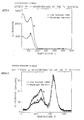
- Each of the specimen crystals was precharacterised by thermoluminescent performance as well as by conduction response by subjecting it to ⁇ irradiation from a 90Sr ⁇ source and ⁇ irradiation from a 60Co source, respectively.
- Thermoluminescence was measured using a Toledo-654 thermoluminescence reader coupled to a Spectrum-88 multichannel analyser, the diamonds being held vertically by the parallel implanted surfaces. Post irradiation TL responses from each of the sides were then recorded on a personal computer for analysis.
- the diamonds were in turn clamped in a probe of the type described in South African patent application no. 93/1541.
- the probe was coupled via a voltage matching interface to a PTW DI/4 dosimeter and ratemeter system and the response of each specimen to irradiation monitored.
- the specimens were maintained at a temperature of 100°C while hydrogen (H+) ions with energy of 50keV and a dose of 5 X 10¹⁶/cm2 were applied to the contact sites on the pairs of opposite and parallel surfaces. Following each hydrogen implantation regime, carbon ions were implanted on to the same surface to provide new ohmic contacts in the manner described above.
- the diamonds were then reirradiated under identical conditions to those used previously and the TL and conduction mode responses measured as before for comparison with the prehydrogenation data generated earlier.
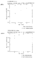
- Figures 3 and 4 indicate the radiation response of the low and higher nitrogen sets of diamonds respectively in conduction mode before and after hydrogenation. Although there was no change in the magnitude of the conduction response, the response time (or rise time) improved significantly after hydrogenation. This improvement and the previously observed drop in thermoluminescence after hydrogenation are ascribed to the passivation of trapping levels in the diamond crystal by the hydrogen.
- the post synthesis hydrogenation treatment of this invention enables highly sensitive radiation detectors with good rise time response to be manufactured routinely.
- the diamond sensor elements may be subjected to a series of hydrogenation steps of the same or of different doses and energies, and the effect of each such step can be conveniently monitored by applying thermoluminescence techniques.
Landscapes
- Physics & Mathematics (AREA)
- Health & Medical Sciences (AREA)
- Life Sciences & Earth Sciences (AREA)
- General Physics & Mathematics (AREA)
- High Energy & Nuclear Physics (AREA)
- Molecular Biology (AREA)
- Spectroscopy & Molecular Physics (AREA)
- Crystals, And After-Treatments Of Crystals (AREA)
- Measurement Of Radiation (AREA)
Applications Claiming Priority (2)
| Application Number | Priority Date | Filing Date | Title |
|---|---|---|---|
| ZA935877 | 1993-08-12 | ||
| ZA935877 | 1993-08-12 |
Publications (3)
| Publication Number | Publication Date |
|---|---|
| EP0638825A2 true EP0638825A2 (de) | 1995-02-15 |
| EP0638825A3 EP0638825A3 (de) | 1995-11-15 |
| EP0638825B1 EP0638825B1 (de) | 1998-10-14 |
Family
ID=25583121
Family Applications (1)
| Application Number | Title | Priority Date | Filing Date |
|---|---|---|---|
| EP94305975A Expired - Lifetime EP0638825B1 (de) | 1993-08-12 | 1994-08-12 | Verfahren zur Erkennung von ionisierender Strahlung |
Country Status (5)
| Country | Link |
|---|---|
| US (1) | US5527565A (de) |
| EP (1) | EP0638825B1 (de) |
| JP (1) | JPH07167959A (de) |
| DE (1) | DE69413907T2 (de) |
| ZA (1) | ZA946002B (de) |
Cited By (2)
| Publication number | Priority date | Publication date | Assignee | Title |
|---|---|---|---|---|
| US5773830A (en) * | 1993-07-20 | 1998-06-30 | Saint-Gobain/Norton Industrial Ceramics Corp. | CVD diamond radiation detector |
| EP0833377A3 (de) * | 1996-09-30 | 1999-08-18 | Xerox Corporation | Verbesserte Hydrogenierung von mit einem Oxyd eingekapseltem Material. |
Families Citing this family (3)
| Publication number | Priority date | Publication date | Assignee | Title |
|---|---|---|---|---|
| GB0220767D0 (en) * | 2002-09-06 | 2002-10-16 | Diamanx Products Ltd | Diamond radiation detector |
| US7481879B2 (en) * | 2004-01-16 | 2009-01-27 | Sumitomo Electric Industries, Ltd. | Diamond single crystal substrate manufacturing method and diamond single crystal substrate |
| JP5096747B2 (ja) * | 2006-03-02 | 2012-12-12 | 株式会社神戸製鋼所 | ビーム検出部材およびそれを用いたビーム検出器 |
Family Cites Families (11)
| Publication number | Priority date | Publication date | Assignee | Title |
|---|---|---|---|---|
| US3824680A (en) * | 1968-03-28 | 1974-07-23 | Levina Fizichesky I I Lebedeva | Nuclear radiation detector and method of manufacturing same |
| ZA747725B (en) * | 1974-12-04 | 1976-07-28 | De Beers Ind Diamond | Improvements in or relating to diamonds |
| NL8006321A (nl) * | 1980-11-19 | 1982-06-16 | Eduard Anton Burgemeister | Werkwijze en inrichting voor het detecteren van ioniserende straling. |
| IL81537A (en) * | 1986-02-24 | 1991-05-12 | De Beers Ind Diamond | Method and synthetic diamond detector for detection of nuclear radiation |
| ZA874362B (en) * | 1986-06-20 | 1988-02-24 | De Beers Ind Diamond | Forming contacts on diamonds |
| JPH01246116A (ja) * | 1988-03-29 | 1989-10-02 | Natl Inst For Res In Inorg Mater | 針状,繊維状,多孔質状ダイヤモンドまたはそれらの集合体の製造法 |
| EP0384084B1 (de) * | 1988-12-28 | 1993-06-16 | De Beers Industrial Diamond Division (Proprietary) Limited | Diamant-Szintillationsdetektor |
| GB8902443D0 (en) * | 1989-02-03 | 1989-03-22 | Jones Barbara L | Radiation detector |
| US5079425A (en) * | 1990-01-10 | 1992-01-07 | Sumitomo Electric Industries, Ltd. | Radiation detecting element |
| GB9021689D0 (en) * | 1990-10-05 | 1990-11-21 | De Beers Ind Diamond | Diamond neutron detector |
| GB9205458D0 (en) * | 1992-03-12 | 1992-04-22 | De Beers Ind Diamond | Radiation probe |
-
1994
- 1994-08-10 ZA ZA946002A patent/ZA946002B/xx unknown
- 1994-08-12 EP EP94305975A patent/EP0638825B1/de not_active Expired - Lifetime
- 1994-08-12 DE DE69413907T patent/DE69413907T2/de not_active Expired - Fee Related
- 1994-08-12 JP JP6190384A patent/JPH07167959A/ja active Pending
- 1994-08-12 US US08/289,527 patent/US5527565A/en not_active Expired - Fee Related
Cited By (2)
| Publication number | Priority date | Publication date | Assignee | Title |
|---|---|---|---|---|
| US5773830A (en) * | 1993-07-20 | 1998-06-30 | Saint-Gobain/Norton Industrial Ceramics Corp. | CVD diamond radiation detector |
| EP0833377A3 (de) * | 1996-09-30 | 1999-08-18 | Xerox Corporation | Verbesserte Hydrogenierung von mit einem Oxyd eingekapseltem Material. |
Also Published As
| Publication number | Publication date |
|---|---|
| EP0638825A3 (de) | 1995-11-15 |
| EP0638825B1 (de) | 1998-10-14 |
| JPH07167959A (ja) | 1995-07-04 |
| DE69413907D1 (de) | 1998-11-19 |
| US5527565A (en) | 1996-06-18 |
| DE69413907T2 (de) | 1999-04-22 |
| ZA946002B (en) | 1995-03-14 |
Similar Documents
| Publication | Publication Date | Title |
|---|---|---|
| Dozier et al. | Photon energy dependence of radiation effects in MOS structures | |
| Polman et al. | Defect states of amorphous Si probed by the diffusion and solubility of Cu | |
| Tromson et al. | Thermally stimulated current investigations on diamond x-ray detectors | |
| EP0250252B1 (de) | Verfahren zur Herstellung eines Kontaktes auf einem Diamant | |
| Agersnap Larsen et al. | Thermally stimulated conductivity and thermoluminescence from Al2O3: C | |
| Keddy et al. | Synthetic diamonds as ionisation chamber radiation detectors in biological environments | |
| EP0638825B1 (de) | Verfahren zur Erkennung von ionisierender Strahlung | |
| Nam et al. | The effects of nitrogen impurity on the radiation detection properties of synthetic diamond | |
| Achtziger et al. | Recoil implantation of radioactive transition metals and their investigation in silicon by deep‐level transient spectroscopy | |
| Schirru et al. | Radiation detector performances of nitrogen doped HPHT diamond films | |
| Hafez et al. | The TL-properties of some environmental materials and assessment the effects of other different parameters | |
| Deicher et al. | Detection of electronic perturbations in silicon after EC decay of 111In observed by PAC | |
| JPH0542399B2 (de) | ||
| Assiamah et al. | A synthetic diamond probe for low-energy X-ray dose measurements | |
| Bridges | Paraelectric Resonance of Ag+ in RbCl | |
| Abdel-Rahmana et al. | Evaluating the Dosimetric and Sensitivity Mapping Performance of CVD Diamond Radiation Detector with X-Ray Tube and Dual Synchrotron Micro-Beams | |
| Kada et al. | Investigation of electrically-active deep levels in single-crystalline diamond by particle-induced charge transient spectroscopy | |
| Rauhala et al. | Defect formation and annealing behavior of InP implanted by low-energy N 15 ions | |
| Blosse et al. | Defects in pulsed laser and thermal processed ion implanted silicon | |
| Hage-Ali et al. | Characterization of CdTe nuclear detector materials | |
| Toney et al. | Composition and performance mapping of CdZnTe nuclear spectrometers | |
| Cordeiro et al. | Study of defects in Silicon by means of Perturbed Angular gamma-gamma Correlation Spectroscopy | |
| SU991836A1 (ru) | Способ отбора алмазов дл детекторов ионизирующих излучений | |
| Bergholz et al. | Reactions of cobalt in silicon with electron-irradiation-induced defects | |
| Kim et al. | Epitaxial integrated dE1− dE2 silicon detectors |
Legal Events
| Date | Code | Title | Description |
|---|---|---|---|
| PUAI | Public reference made under article 153(3) epc to a published international application that has entered the european phase |
Free format text: ORIGINAL CODE: 0009012 |
|
| AK | Designated contracting states |
Kind code of ref document: A2 Designated state(s): BE CH DE FR GB IT LI NL SE |
|
| PUAL | Search report despatched |
Free format text: ORIGINAL CODE: 0009013 |
|
| AK | Designated contracting states |
Kind code of ref document: A3 Designated state(s): BE CH DE FR GB IT LI NL SE |
|
| 17P | Request for examination filed |
Effective date: 19960415 |
|
| GRAG | Despatch of communication of intention to grant |
Free format text: ORIGINAL CODE: EPIDOS AGRA |
|
| 17Q | First examination report despatched |
Effective date: 19970930 |
|
| GRAG | Despatch of communication of intention to grant |
Free format text: ORIGINAL CODE: EPIDOS AGRA |
|
| GRAH | Despatch of communication of intention to grant a patent |
Free format text: ORIGINAL CODE: EPIDOS IGRA |
|
| GRAG | Despatch of communication of intention to grant |
Free format text: ORIGINAL CODE: EPIDOS AGRA |
|
| GRAH | Despatch of communication of intention to grant a patent |
Free format text: ORIGINAL CODE: EPIDOS IGRA |
|
| RAP1 | Party data changed (applicant data changed or rights of an application transferred) |
Owner name: DE BEERS INDUSTRIAL DIAMOND DIVISION (PROPRIETARY) |
|
| GRAH | Despatch of communication of intention to grant a patent |
Free format text: ORIGINAL CODE: EPIDOS IGRA |
|
| GRAA | (expected) grant |
Free format text: ORIGINAL CODE: 0009210 |
|
| AK | Designated contracting states |
Kind code of ref document: B1 Designated state(s): BE CH DE FR GB IT LI NL SE |
|
| PG25 | Lapsed in a contracting state [announced via postgrant information from national office to epo] |
Ref country code: LI Free format text: LAPSE BECAUSE OF FAILURE TO SUBMIT A TRANSLATION OF THE DESCRIPTION OR TO PAY THE FEE WITHIN THE PRESCRIBED TIME-LIMIT Effective date: 19981014 Ref country code: CH Free format text: LAPSE BECAUSE OF FAILURE TO SUBMIT A TRANSLATION OF THE DESCRIPTION OR TO PAY THE FEE WITHIN THE PRESCRIBED TIME-LIMIT Effective date: 19981014 Ref country code: BE Free format text: LAPSE BECAUSE OF FAILURE TO SUBMIT A TRANSLATION OF THE DESCRIPTION OR TO PAY THE FEE WITHIN THE PRESCRIBED TIME-LIMIT Effective date: 19981014 |
|
| REG | Reference to a national code |
Ref country code: CH Ref legal event code: EP |
|
| REF | Corresponds to: |
Ref document number: 69413907 Country of ref document: DE Date of ref document: 19981119 |
|
| PG25 | Lapsed in a contracting state [announced via postgrant information from national office to epo] |
Ref country code: SE Free format text: LAPSE BECAUSE OF FAILURE TO SUBMIT A TRANSLATION OF THE DESCRIPTION OR TO PAY THE FEE WITHIN THE PRESCRIBED TIME-LIMIT Effective date: 19990114 |
|
| ET | Fr: translation filed | ||
| REG | Reference to a national code |
Ref country code: CH Ref legal event code: PL |
|
| PLBE | No opposition filed within time limit |
Free format text: ORIGINAL CODE: 0009261 |
|
| STAA | Information on the status of an ep patent application or granted ep patent |
Free format text: STATUS: NO OPPOSITION FILED WITHIN TIME LIMIT |
|
| 26N | No opposition filed | ||
| REG | Reference to a national code |
Ref country code: GB Ref legal event code: IF02 |
|
| PGFP | Annual fee paid to national office [announced via postgrant information from national office to epo] |
Ref country code: GB Payment date: 20030806 Year of fee payment: 10 |
|
| PGFP | Annual fee paid to national office [announced via postgrant information from national office to epo] |
Ref country code: FR Payment date: 20030808 Year of fee payment: 10 |
|
| PGFP | Annual fee paid to national office [announced via postgrant information from national office to epo] |
Ref country code: DE Payment date: 20030822 Year of fee payment: 10 |
|
| PGFP | Annual fee paid to national office [announced via postgrant information from national office to epo] |
Ref country code: NL Payment date: 20030831 Year of fee payment: 10 |
|
| PG25 | Lapsed in a contracting state [announced via postgrant information from national office to epo] |
Ref country code: GB Free format text: LAPSE BECAUSE OF NON-PAYMENT OF DUE FEES Effective date: 20040812 |
|
| PG25 | Lapsed in a contracting state [announced via postgrant information from national office to epo] |
Ref country code: NL Free format text: LAPSE BECAUSE OF NON-PAYMENT OF DUE FEES Effective date: 20050301 Ref country code: DE Free format text: LAPSE BECAUSE OF NON-PAYMENT OF DUE FEES Effective date: 20050301 |
|
| GBPC | Gb: european patent ceased through non-payment of renewal fee |
Effective date: 20040812 |
|
| PG25 | Lapsed in a contracting state [announced via postgrant information from national office to epo] |
Ref country code: FR Free format text: LAPSE BECAUSE OF NON-PAYMENT OF DUE FEES Effective date: 20050429 |
|
| NLV4 | Nl: lapsed or anulled due to non-payment of the annual fee |
Effective date: 20050301 |
|
| REG | Reference to a national code |
Ref country code: FR Ref legal event code: ST |
|
| PG25 | Lapsed in a contracting state [announced via postgrant information from national office to epo] |
Ref country code: IT Free format text: LAPSE BECAUSE OF NON-PAYMENT OF DUE FEES;WARNING: LAPSES OF ITALIAN PATENTS WITH EFFECTIVE DATE BEFORE 2007 MAY HAVE OCCURRED AT ANY TIME BEFORE 2007. THE CORRECT EFFECTIVE DATE MAY BE DIFFERENT FROM THE ONE RECORDED. Effective date: 20050812 |