EP0638867A2 - Réseau de communication entre processeurs à reconfiguration dynamique pour des multiprocesseurs de type SIMD et appareil pour sa mise en oeuvre - Google Patents
Réseau de communication entre processeurs à reconfiguration dynamique pour des multiprocesseurs de type SIMD et appareil pour sa mise en oeuvre Download PDFInfo
- Publication number
- EP0638867A2 EP0638867A2 EP94112550A EP94112550A EP0638867A2 EP 0638867 A2 EP0638867 A2 EP 0638867A2 EP 94112550 A EP94112550 A EP 94112550A EP 94112550 A EP94112550 A EP 94112550A EP 0638867 A2 EP0638867 A2 EP 0638867A2
- Authority
- EP
- European Patent Office
- Prior art keywords
- data
- configuration register
- controller
- group
- processing elements
- Prior art date
- Legal status (The legal status is an assumption and is not a legal conclusion. Google has not performed a legal analysis and makes no representation as to the accuracy of the status listed.)
- Withdrawn
Links
Images




Classifications
-
- G—PHYSICS
- G06—COMPUTING OR CALCULATING; COUNTING
- G06F—ELECTRIC DIGITAL DATA PROCESSING
- G06F15/00—Digital computers in general; Data processing equipment in general
- G06F15/16—Combinations of two or more digital computers each having at least an arithmetic unit, a program unit and a register, e.g. for a simultaneous processing of several programs
- G06F15/163—Interprocessor communication
- G06F15/173—Interprocessor communication using an interconnection network, e.g. matrix, shuffle, pyramid, star, snowflake
- G06F15/17337—Direct connection machines, e.g. completely connected computers, point to point communication networks
- G06F15/17343—Direct connection machines, e.g. completely connected computers, point to point communication networks wherein the interconnection is dynamically configurable, e.g. having loosely coupled nearest neighbor architecture
-
- G—PHYSICS
- G06—COMPUTING OR CALCULATING; COUNTING
- G06F—ELECTRIC DIGITAL DATA PROCESSING
- G06F15/00—Digital computers in general; Data processing equipment in general
- G06F15/16—Combinations of two or more digital computers each having at least an arithmetic unit, a program unit and a register, e.g. for a simultaneous processing of several programs
- G06F15/163—Interprocessor communication
- G06F15/173—Interprocessor communication using an interconnection network, e.g. matrix, shuffle, pyramid, star, snowflake
- G06F15/17356—Indirect interconnection networks
- G06F15/17368—Indirect interconnection networks non hierarchical topologies
- G06F15/17381—Two dimensional, e.g. mesh, torus
Definitions
- This invention relates in general to computer architectures, and, more particularly, to a dynamically reconfigurable switching means useful in connecting processing elements in processor arrays in SIMD multi-processor architectures.
- This invention describes a dynamically reconfigurable interprocessor communication network for dynamically controlling data flow between processing elements in processor arrays found in parallel Single Instruction stream Multiple Data stream (SIMD) computer architectures.
- SIMD Single Instruction stream Multiple Data stream
- DRS Dynamically Reconfigurable Switch
- PE processing Elements
- a number of important and novel architectural features are attained through the use of the present invention. These include: requiring a minimal number of interprocessor connections per PE and allowing for local communication autonomy at the level of each PE. The former is important from a physical implementation point of view, and the later is significant for adding a new dimension of flexibility to existing SIMD architectures.
- Dynamic reconfigurability of the processing elements in the processing array is achieved by associating with each PE a distinct DRS embodying the present invention.
- the configuration of the DRS i.e., switch settings required to pass data from an input port to an output port, can be either set by the instructions received by all PEs (broadcast instructions) from the controller, or be independently set to a value stored locally in each PE's memory area. Special consideration has been made with respect to cascading issues arising when data is communicated with PEs forming the processing array located in different physical chips forming partitions of the processor array.
- At least two primary features of this invention set it apart from other more conventional interprocessor communication schemes.
- the design of the present invention is very efficient in using interprocessor communication links by exploiting certain communication constraints.
- this design only four bidirectional connections are required per PE to implement direct eight nearest neighbor communications.
- only a single bidirectional wire per data path bit is required to communicate between corresponding switches in neighboring chips or across partition boundaries. Consequently, the number of pins required for interprocessor communication across chip boundaries is reduced, allowing for more PEs to be implemented on a given chip.
- the second significant feature of this design is the added communication flexibility achieved from dynamic reconfigurability of the DRS during processing.
- data movement between PEs is accomplished in a homogeneous fashion, see Figures 5A and 5B.
- a pre-selected direction e.g., North, East, South, West, etc.
- each PE can independently set a specific direction for transfer of data to, or from, its neighboring PEs.
- This ability to dynamically reconfigure and direct data flow during processing allows for construction of complex computational paths which better match a specific algorithm. See Figures 6A and 6B.
- mapping methods have been developed to efficiently take advantage of this dynamic reconfigurability of data flow through a processing array for efficiently processing neural network algorithms. Similar dynamic mapping methods can potentially be generalized to address problems in other fields.
- the present invention is found to be embodied in a SIMD architecture having a two dimensional array of processing elements, where a controller broadcasts instructions to all processing elements in the array, a dynamically reconfigurable switching means useful to connect four of the processing elements in the array into a group in accordance with either the broadcast instruction of the controller or a special communication instruction held in one processing element of the group, and would include at least one dataline being at least one bit wide, connected to each processing element in the group.
- a multiplexer unit is connected to each data line, the controller and to a configuration register.
- a demultiplexer unit is connected to each data line, the controller and to the configuration register, as well as to the source output port of the multiplexer unit.
- the demultiplexer is adapted to operate in accord with either the broadcast instruction from the controller or the contents of the configuration register to select one of the four data lines and applying the data from the source output port of the multiplexer unit thereto.
- the present invention is also embodied in a SIMD architecture having a two dimensional array of processing elements, with multiple chips containing the processing elements of the array, where a controller broadcasts instructions to all processing elements in the array, a dynamically reconfigurable switching means useful to connect four of the processing elements in the array into a group which may cross chip boundaries to form partitions with each partition associated with one chip, to direct data movement dynamically between selected processing elements of the group in accordance with either the broadcast instruction of the controller or a special communication instruction held in one processing element of the group.
- the switch would include, in each partition, at least one dataline connected to each processing element in the group in the partition.
- a multiplexer unit is connected to each data line, the controller and to a configuration register.
- a demultiplexer unit is connected to each data line, the controller, the configuration register, and to the source output port of the multiplexer unit.
- the demultiplexer is adapted to operate in accord with either the broadcast instruction from the controller or the contents of the configuration register to select one of the four data lines and applying the data from the source output port of the multiplexer thereto.
- a dataline connects each multiplexer in one partition to the demultiplexer in the same partition, and a crossing dataline connects each multiplexer in one partition to the demultiplexer in each other partition.
- the demultiplexer unit can also be adapted to operate in accord with either the broadcast instruction from the controller or the contents of the configuration register to apply the data from the source output port of the multiplexer means to at least two of the data lines.
- the dataline connecting each multiplexer unit in one partition to the demultiplexer unit in the same partition and the crossing dataline connecting each multiplexer in one partition to the demultiplexer in each other partition may be a single dataline.
- the present invention is also embodied in a dynamically reconfigurable switching means that further includes between one and four of such switches in a configuration as shown in Figure 2A.
- the processing element has at least one input and one output register associated with its input/output data lines.
- each switch in the group has its own dedicated configuration register which can be loaded by any of the processing elements in its group.
- a preferred embodiment of the present invention is found in a computer architecture that can roughly be classified as a Single Instruction stream Multiple Data streams (SIMD) medium or fine grain parallel computer.
- SIMD Single Instruction stream Multiple Data streams
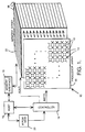
- the top level architecture of such an embodiment is depicted in Figure 1 where each Processing Element 10 is arranged on a two dimensional lattice 12 and is connected to eight of its closest neighbors through four programmable switches 14.
- the architecture is most easily discussed in three major units: the host computer 16, the controller 18, and the Processor Array 20. Its memory can be accessed by the host computer 16 through the use of high speed Direct Memory Access (DMA) channel.
- DMA Direct Memory Access
- the host computer 16 needs only to specify the memory location of the data block to be accessed in the memory space and the number of words to be transferred.
- the DMA controller 19 can transfer the data without using any additional cycles from the host computer 16. This feature permits simple programming interface between the host 16 and the coprocessor.
- the host computer 16 is primarily used for properly formatting the input data, long term storage of data, and as a visual interface between the user and the invention.
- the controller unit 18 interfaces to both the host computer 16 and to the Processor Array 20.
- the controller 18 contains a microprogram memory area 23 that can be accessed by the host 16. High level programs can be written and compiled on the host 16 and the generated control information can be down loaded from the host 16 to the microprogram memory 23 of the controller 18.
- the controller 18 broadcasts an instruction and a memory address to the Processor Array 20 during each processing cycle.
- the processors 10 in the Processor Array 20 perform operations received from the controller 18 based on a mask flag available in each Processing Element 10.
- the Processor Array unit 20 contains all the processing elements 10 and the supporting interconnection switches 14. Each Processing Element 10 in the Processor Array 20 has direct access to its local column of memory within the architecture's memory space 22. Due to this distributed memory organization, memory conflicts are eliminated which consequently simplifies both the hardware and the software designs.
- the Processing Element 10 makes up the computational engine of the system.
- the processing Elements 10 are part of the Processor Array 20 subsystem and all receive the same instruction stream, but perform the required operations on their own local data stream.
- Each processing Element 10 is comprised of a number of Functional Units 24, a small register file 26, interprocessor communication ports 28, and a mask flag 30 as illustrated in FIG. 4.
- each Processing Element 10 includes an adder, multiplier, shift/logic unit. Depending on the specific implementation, additional functional units 24 can be added to the design. Similar to many RISC type processors, each Processing Element 10 has an internal data bus 32 to transfer data between various units. For example, data could move from a register in the register file 26 to one of the operand registers of the adder unit, or data can be transferred from the output register of the multiplier to the I/O output port 28. A mask bit is used to enable/disable the functional units 24 from performing the operation instructed by the controller 18.
- Each Processing Element 10 communicates with its neighbors through the I/O ports 28 . Only one input and one output port 28 is required in each Processing Element 10 since during each systolic cycle only a single data value is received and transmitted by a Processing Element 10. In configurations utilizing more than one switch, such as the one shown in FIG. 2A, multiple Input/Output ports can be used for simultaneous data transfer between members of a group.
- the output of each of the I/O registers is connected to the four switches 14 surrounding each Processing Element 10. The selection of the destination Processing Element 10 for an outgoing data value and the source Processing Element 10 for an incoming data value is made by the specific switch settings of the switches 14.
- Each processor 10 in the architecture has read/write access to its own local memory area 38 as shown in FIG. 4.
- the memory can be kept off chip in order to allow for simple memory expansion.
- the memory location associated with each instruction is broadcasted by the controller 18 unit to all the Processing Elements 10.
- all the processors 10 can access a single plane of memory at each time step.
- the memory access speed is matched with the computation rate of each processor 10 so that each memory access can be completely overlapped with computation. This feature allows for efficient systolic processing.
- Each word in the Processing Element's local memory area 38 is preferably comprised of two distinct fields 40, 42.
- the first 40 is the data field used to store and retrieve the actual data associated with the computation, such as neuron activation values, synaptic weight values, etc..
- the second field 42 holds three bits which indicate the switch setting for the switch 14 associated with each Processing Element 10.
- the three configuration bits can be decoded to select one of the eight configurations shown in FIG. 7. These switch setting values are determined prior to the start of computation and are preloaded by the host 16. A new switch setting value can be read during each instruction cycle.
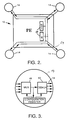
- Nearest neighbor communications in the Processor Array 20 are performed through dynamically reconfigurable switches 14 connecting one Processing Element 10 to three of its eight nearest neighbors. There are four switches 14 connected to each Processing Element 10, see Figure 2.
- FIG. 2A An alternate configuration for nearest neighbor communications in the Processor Array 20 is shown in Figure 2A where up to four dynamically reconfigurable switches 14 are used in each group of four processing elements.
- each processing element 10 has at least one input and one output register associated with its input/output data lines.
- two simultaneous data transfers can be implemented from any pair of processing elements in the group, to any other pair of processing elements in the same group.
- each switch in the group has its own dedicated configuration register which can be loaded by any of the processing elements in its group.
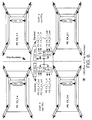
- dynamically reconfigurable switch 14 allows for communication between four nearest-neighbor Processing Elements 10 while only requiring at least one I/O connection 54 to each Processing Element 10.
- the communication bandwidth between adjacent Processing Elements 10 are kept equal to the memory access bandwidth to assure efficient systolic processing.
- One unique feature of the present architecture is to allow each switch 14 in the interconnection network to be distinctly configured.
- the switch settings are stored in the local memory 38 of each switch 14 and can be accessed at the beginning of each processing cycle.
- the switch memory address is supplied by the controller 18 at each cycle.
- This design allows for a dynamically changing flow pattern of data through the processing array 20.
- all the Processing Elements 10 perform the same communication operation.
- the instruction word broadcasted by the controller 18 specifies which direction the data is to be moved in the processing array 20, e.g., North to South, East to West, West to South, etc.
- one Processing Element 10 can receive data from its North Neighbor while another is receiving data from its West Neighbor, depending on the local switch settings.
- FIG. 3 An example implementation of this switch 14 is shown in Figure 3 using a multiplexer 48 and demultiplexer 50 to select one of four inputs and route the data to one of four outputs 54.
- This flexibility in interprocessor communication is essential in efficiently implementing neural networks with sparse or block structured interconnections.
- DRS Dynamically Reconfigurable Switches
- a configuration register within the DRS controls the selection of source and destination ports for the data flowing through the switch.
- the content of this configuration register can be set by only one of the processing elements connected to the switch, e.g., the upper left Processing Element of the DRS.
- a by-pass mode may be implemented so that the data movement direction is supplied by the specific communication instruction.
- data movement in the processor array is homogeneous, like that of conventional SIMD parallel processors.
- the instruction specifies the direction of data movement for all the Processing Elements in the system. See Figures 5A and 5B.
- inhomogeneous communication patterns can be formed on the processing array.
- a unique feature of this invention is to allow each switch in the interconnection network to be distinctly configured.
- the configuration register can be configured once at the start of processing to implement a specific communication pattern, such as constructing a one dimensional computational ring on the array as shown in Figure 6A without ever changing during the computation.
- it can be dynamically reconfigured to form complex flow patterns on the processing array for each communication step as shown in Figure 6B.
- the 3-bit Conf_Reg specifies one of eight directions the data is to be moved, e.g., South to North, East to West, West to South (see Figure 7). For a given configuration mode, a multiplexer and demultiplexer are used to select one of four inputs and route the data to one of four outputs as listed in Figure 7. Associated with each Conf_Reg there are additional decoding hardware used to generate the appropriate control signals. For the sake of clarity, these details have been omitted in all the drawings. Each PE is identified in all drawings by its row and column coordinate (r.c.). For example, PE 1.1 represents PE located at row one and column one in the processor Array (PA).
- the DRS bus width is not explicitly defined and can vary from 1 to m bits.
- each PE is identified by its chip number. For example, PE C3_1.n represents PE located on row 1 and column n in chip 3. Similarly, PE C3_1.n_out and PE C3_1.n_in represent output channel and input channel respectively, of this PE.
- FIG. 9 shows North-South partition of the DRS. There is one wire connecting the South side of chip 2 pin #1 (i.e., C2_S1) to the North side of chip 4 pin #1 (i.e., C4_N1).
- the procedure for loading the configuration value into the North-south halves of the DRS is similar to the one described for the West-East direction.
- FIG 10 shows corner partition of the DRS, which spreads over four adjacent corners of four chips.
- Conf_Reg On each corner of the switch.
- the load Conf_Reg instruction will pre-configure the upper-left corner DRS cell to select PE C1_n.n_out, so that all three extra copies of Conf_Reg on each corner of the switch can be initialized.
- pins C2_S1 to C2_Sn are assigned to PE C2_n.1 to PE C2_n.n in chip 2, while pin C2_S0 in chip 2 is assigned to PE C1_n.n located at chip 1 to support its diagonal connection to chip 4, as shown in Figure 10.
- switches containing a multiplexer, demultiplexer, and a configuration register groupings can be used at each switching point in the interconnection network.
- an electronic crossbar communications switch is formed between the four processing elements in the group, allowing for simultaneous communications between all four processing elements in the group.
Landscapes
- Engineering & Computer Science (AREA)
- Computer Hardware Design (AREA)
- Physics & Mathematics (AREA)
- Theoretical Computer Science (AREA)
- Mathematical Physics (AREA)
- Software Systems (AREA)
- General Engineering & Computer Science (AREA)
- General Physics & Mathematics (AREA)
- Multi Processors (AREA)
- Microcomputers (AREA)
Applications Claiming Priority (2)
| Application Number | Priority Date | Filing Date | Title |
|---|---|---|---|
| US10646593A | 1993-08-12 | 1993-08-12 | |
| US106465 | 1993-08-12 |
Publications (2)
| Publication Number | Publication Date |
|---|---|
| EP0638867A2 true EP0638867A2 (fr) | 1995-02-15 |
| EP0638867A3 EP0638867A3 (fr) | 1995-10-18 |
Family
ID=22311550
Family Applications (1)
| Application Number | Title | Priority Date | Filing Date |
|---|---|---|---|
| EP94112550A Withdrawn EP0638867A3 (fr) | 1993-08-12 | 1994-08-11 | Réseau de communication entre processeurs à reconfiguration dynamique pour des multiprocesseurs de type SIMD et appareil pour sa mise en oeuvre. |
Country Status (5)
| Country | Link |
|---|---|
| US (1) | US6145072A (fr) |
| EP (1) | EP0638867A3 (fr) |
| JP (1) | JPH07152722A (fr) |
| CA (1) | CA2129882A1 (fr) |
| IL (1) | IL110634A0 (fr) |
Cited By (42)
| Publication number | Priority date | Publication date | Assignee | Title |
|---|---|---|---|---|
| DE19651075A1 (de) * | 1996-12-09 | 1998-06-10 | Pact Inf Tech Gmbh | Einheit zur Verarbeitung von numerischen und logischen Operationen, zum Einsatz in Prozessoren (CPU's), Mehrrechnersystemen, Datenflußprozessoren (DFP's), digitalen Signal Prozessoren (DSP's) oder dergleichen |
| DE19654846A1 (de) * | 1996-12-27 | 1998-07-09 | Pact Inf Tech Gmbh | Verfahren zum selbständigen dynamischen Umladen von Datenflußprozessoren (DFPs) sowie Bausteinen mit zwei- oder mehrdimensionalen programmierbaren Zellstrukturen (FPGAs, DPGAs, o. dgl.) |
| GB2348984B (en) * | 1999-04-09 | 2004-05-12 | Pixelfusion Ltd | Parallel data processing systems |
| US7506136B2 (en) | 1999-04-09 | 2009-03-17 | Clearspeed Technology Plc | Parallel data processing apparatus |
| US7526630B2 (en) | 1999-04-09 | 2009-04-28 | Clearspeed Technology, Plc | Parallel data processing apparatus |
| US7627736B2 (en) | 1999-04-09 | 2009-12-01 | Clearspeed Technology Plc | Thread manager to control an array of processing elements |
| US7782087B2 (en) | 2002-09-06 | 2010-08-24 | Martin Vorbach | Reconfigurable sequencer structure |
| US7822881B2 (en) | 1996-12-27 | 2010-10-26 | Martin Vorbach | Process for automatic dynamic reloading of data flow processors (DFPs) and units with two- or three-dimensional programmable cell architectures (FPGAs, DPGAs, and the like) |
| US7840842B2 (en) | 2001-09-03 | 2010-11-23 | Martin Vorbach | Method for debugging reconfigurable architectures |
| US7844796B2 (en) | 2001-03-05 | 2010-11-30 | Martin Vorbach | Data processing device and method |
| US7899962B2 (en) | 1996-12-20 | 2011-03-01 | Martin Vorbach | I/O and memory bus system for DFPs and units with two- or multi-dimensional programmable cell architectures |
| US7996827B2 (en) | 2001-08-16 | 2011-08-09 | Martin Vorbach | Method for the translation of programs for reconfigurable architectures |
| US8058899B2 (en) | 2000-10-06 | 2011-11-15 | Martin Vorbach | Logic cell array and bus system |
| US8099618B2 (en) | 2001-03-05 | 2012-01-17 | Martin Vorbach | Methods and devices for treating and processing data |
| US8103853B2 (en) * | 2008-03-05 | 2012-01-24 | The Boeing Company | Intelligent fabric system on a chip |
| US8127061B2 (en) | 2002-02-18 | 2012-02-28 | Martin Vorbach | Bus systems and reconfiguration methods |
| US8156284B2 (en) | 2002-08-07 | 2012-04-10 | Martin Vorbach | Data processing method and device |
| US8209653B2 (en) | 2001-09-03 | 2012-06-26 | Martin Vorbach | Router |
| US8230411B1 (en) | 1999-06-10 | 2012-07-24 | Martin Vorbach | Method for interleaving a program over a plurality of cells |
| US8250503B2 (en) | 2006-01-18 | 2012-08-21 | Martin Vorbach | Hardware definition method including determining whether to implement a function as hardware or software |
| US8281108B2 (en) | 2002-01-19 | 2012-10-02 | Martin Vorbach | Reconfigurable general purpose processor having time restricted configurations |
| US8281265B2 (en) | 2002-08-07 | 2012-10-02 | Martin Vorbach | Method and device for processing data |
| US8301872B2 (en) | 2000-06-13 | 2012-10-30 | Martin Vorbach | Pipeline configuration protocol and configuration unit communication |
| USRE44365E1 (en) | 1997-02-08 | 2013-07-09 | Martin Vorbach | Method of self-synchronization of configurable elements of a programmable module |
| US8686549B2 (en) | 2001-09-03 | 2014-04-01 | Martin Vorbach | Reconfigurable elements |
| US8686475B2 (en) | 2001-09-19 | 2014-04-01 | Pact Xpp Technologies Ag | Reconfigurable elements |
| US8812820B2 (en) | 2003-08-28 | 2014-08-19 | Pact Xpp Technologies Ag | Data processing device and method |
| US8819505B2 (en) | 1997-12-22 | 2014-08-26 | Pact Xpp Technologies Ag | Data processor having disabled cores |
| US8914590B2 (en) | 2002-08-07 | 2014-12-16 | Pact Xpp Technologies Ag | Data processing method and device |
| US9037807B2 (en) | 2001-03-05 | 2015-05-19 | Pact Xpp Technologies Ag | Processor arrangement on a chip including data processing, memory, and interface elements |
| US9201828B2 (en) | 2012-10-23 | 2015-12-01 | Analog Devices, Inc. | Memory interconnect network architecture for vector processor |
| US9342306B2 (en) | 2012-10-23 | 2016-05-17 | Analog Devices Global | Predicate counter |
| CN107003982B (zh) * | 2014-12-24 | 2021-07-20 | 英特尔公司 | 用于使用多个多点总线的装置和方法 |
| US11157806B2 (en) | 2017-04-17 | 2021-10-26 | Cerebras Systems Inc. | Task activating for accelerated deep learning |
| US11232348B2 (en) | 2017-04-17 | 2022-01-25 | Cerebras Systems Inc. | Data structure descriptors for deep learning acceleration |
| US11321087B2 (en) | 2018-08-29 | 2022-05-03 | Cerebras Systems Inc. | ISA enhancements for accelerated deep learning |
| US11328207B2 (en) | 2018-08-28 | 2022-05-10 | Cerebras Systems Inc. | Scaled compute fabric for accelerated deep learning |
| US11328208B2 (en) | 2018-08-29 | 2022-05-10 | Cerebras Systems Inc. | Processor element redundancy for accelerated deep learning |
| US11488004B2 (en) | 2017-04-17 | 2022-11-01 | Cerebras Systems Inc. | Neuron smearing for accelerated deep learning |
| US11934945B2 (en) | 2017-02-23 | 2024-03-19 | Cerebras Systems Inc. | Accelerated deep learning |
| US12169771B2 (en) | 2019-10-16 | 2024-12-17 | Cerebras Systems Inc. | Basic wavelet filtering for accelerated deep learning |
| US12177133B2 (en) | 2019-10-16 | 2024-12-24 | Cerebras Systems Inc. | Dynamic routing for accelerated deep learning |
Families Citing this family (108)
| Publication number | Priority date | Publication date | Assignee | Title |
|---|---|---|---|---|
| US5956518A (en) | 1996-04-11 | 1999-09-21 | Massachusetts Institute Of Technology | Intermediate-grain reconfigurable processing device |
| US6101319A (en) * | 1997-01-02 | 2000-08-08 | Intel Corporation | Method and apparatus for the automatic configuration of strapping options on a circuit board assembly |
| US9092595B2 (en) | 1997-10-08 | 2015-07-28 | Pact Xpp Technologies Ag | Multiprocessor having associated RAM units |
| US6167502A (en) * | 1997-10-10 | 2000-12-26 | Billions Of Operations Per Second, Inc. | Method and apparatus for manifold array processing |
| US6051030A (en) * | 1998-03-31 | 2000-04-18 | International Business Machines Corporation | Emulation module having planar array organization |
| US6167501A (en) * | 1998-06-05 | 2000-12-26 | Billions Of Operations Per Second, Inc. | Methods and apparatus for manarray PE-PE switch control |
| US6839728B2 (en) * | 1998-10-09 | 2005-01-04 | Pts Corporation | Efficient complex multiplication and fast fourier transform (FFT) implementation on the manarray architecture |
| US6539027B1 (en) * | 1999-01-19 | 2003-03-25 | Coastcom | Reconfigurable, intelligent signal multiplexer and network design and maintenance system therefor |
| KR100300338B1 (ko) * | 1999-02-19 | 2001-09-26 | 박래홍 | 2차원 이산 웨이브렛 변환을 위한 초고밀도 집적회로 구조 |
| JP3674515B2 (ja) * | 2000-02-25 | 2005-07-20 | 日本電気株式会社 | アレイ型プロセッサ |
| US6912626B1 (en) * | 2000-08-31 | 2005-06-28 | Micron Technology, Inc. | Method and apparatus for connecting a massively parallel processor array to a memory array in a bit serial manner |
| US9436631B2 (en) | 2001-03-05 | 2016-09-06 | Pact Xpp Technologies Ag | Chip including memory element storing higher level memory data on a page by page basis |
| US9141390B2 (en) | 2001-03-05 | 2015-09-22 | Pact Xpp Technologies Ag | Method of processing data with an array of data processors according to application ID |
| US9250908B2 (en) | 2001-03-05 | 2016-02-02 | Pact Xpp Technologies Ag | Multi-processor bus and cache interconnection system |
| US9552047B2 (en) | 2001-03-05 | 2017-01-24 | Pact Xpp Technologies Ag | Multiprocessor having runtime adjustable clock and clock dependent power supply |
| US10031733B2 (en) | 2001-06-20 | 2018-07-24 | Scientia Sol Mentis Ag | Method for processing data |
| JP3921367B2 (ja) * | 2001-09-26 | 2007-05-30 | 日本電気株式会社 | データ処理装置および方法、コンピュータプログラム、情報記憶媒体、並列演算装置、データ処理システム |
| JP3693013B2 (ja) * | 2001-12-26 | 2005-09-07 | 日本電気株式会社 | データ処理システム、アレイ型プロセッサ、データ処理装置、コンピュータプログラム、情報記憶媒体 |
| US7085913B2 (en) * | 2002-02-13 | 2006-08-01 | International Business Machines Corporation | Hub/router for communication between cores using cartesian coordinates |
| US6906978B2 (en) * | 2002-03-19 | 2005-06-14 | Intel Corporation | Flexible integrated memory |
| US9170812B2 (en) | 2002-03-21 | 2015-10-27 | Pact Xpp Technologies Ag | Data processing system having integrated pipelined array data processor |
| US7180854B2 (en) * | 2002-04-10 | 2007-02-20 | Keith Cambron | Route on failure method and apparatus for automatic rerouting network traffic through a reconfigurable, intelligent signal multiplexer upon failures of multiplexer components or of network spans |
| US7461234B2 (en) * | 2002-07-01 | 2008-12-02 | Panasonic Corporation | Loosely-biased heterogeneous reconfigurable arrays |
| US7464311B2 (en) * | 2002-08-05 | 2008-12-09 | Mitsubishi Denki Kabushiki Kaisha | Apparatus and method for device selective scans in data streaming test environment for a processing unit having multiple cores |
| JP3987783B2 (ja) * | 2002-10-11 | 2007-10-10 | Necエレクトロニクス株式会社 | アレイ型プロセッサ |
| JP3987784B2 (ja) * | 2002-10-30 | 2007-10-10 | Necエレクトロニクス株式会社 | アレイ型プロセッサ |
| US7340644B2 (en) * | 2002-12-02 | 2008-03-04 | Marvell World Trade Ltd. | Self-reparable semiconductor and method thereof |
| US20060001669A1 (en) * | 2002-12-02 | 2006-01-05 | Sehat Sutardja | Self-reparable semiconductor and method thereof |
| US7185225B2 (en) * | 2002-12-02 | 2007-02-27 | Marvell World Trade Ltd. | Self-reparable semiconductor and method thereof |
| US7673118B2 (en) | 2003-02-12 | 2010-03-02 | Swarztrauber Paul N | System and method for vector-parallel multiprocessor communication |
| US6954085B2 (en) * | 2003-10-13 | 2005-10-11 | International Business Machines Corporation | System and method for dynamically executing a function in a programmable logic array |
| US7937557B2 (en) | 2004-03-16 | 2011-05-03 | Vns Portfolio Llc | System and method for intercommunication between computers in an array |
| US20080235490A1 (en) * | 2004-06-18 | 2008-09-25 | Anthony Mark Jones | System for configuring a processor array |
| US8103866B2 (en) * | 2004-06-18 | 2012-01-24 | Nethra Imaging Inc. | System for reconfiguring a processor array |
| JP4477959B2 (ja) * | 2004-07-26 | 2010-06-09 | 独立行政法人理化学研究所 | ブロードキャスト型並列処理のための演算処理装置 |
| JP2006236106A (ja) * | 2005-02-25 | 2006-09-07 | Canon Inc | データ処理装置及びデータ処理方法 |
| US8024549B2 (en) * | 2005-03-04 | 2011-09-20 | Mtekvision Co., Ltd. | Two-dimensional processor array of processing elements |
| US7814242B1 (en) * | 2005-03-25 | 2010-10-12 | Tilera Corporation | Managing data flows in a parallel processing environment |
| US8443169B2 (en) * | 2005-03-28 | 2013-05-14 | Gerald George Pechanek | Interconnection network connecting operation-configurable nodes according to one or more levels of adjacency in multiple dimensions of communication in a multi-processor and a neural processor |
| US7904695B2 (en) * | 2006-02-16 | 2011-03-08 | Vns Portfolio Llc | Asynchronous power saving computer |
| JP4536618B2 (ja) * | 2005-08-02 | 2010-09-01 | 富士通セミコンダクター株式会社 | リコンフィグ可能な集積回路装置 |
| US7904615B2 (en) * | 2006-02-16 | 2011-03-08 | Vns Portfolio Llc | Asynchronous computer communication |
| US7617383B2 (en) * | 2006-02-16 | 2009-11-10 | Vns Portfolio Llc | Circular register arrays of a computer |
| US7966481B2 (en) | 2006-02-16 | 2011-06-21 | Vns Portfolio Llc | Computer system and method for executing port communications without interrupting the receiving computer |
| US7636835B1 (en) * | 2006-04-14 | 2009-12-22 | Tilera Corporation | Coupling data in a parallel processing environment |
| US7539845B1 (en) * | 2006-04-14 | 2009-05-26 | Tilera Corporation | Coupling integrated circuits in a parallel processing environment |
| US7577820B1 (en) | 2006-04-14 | 2009-08-18 | Tilera Corporation | Managing data in a parallel processing environment |
| JP2007293701A (ja) * | 2006-04-26 | 2007-11-08 | Canon Inc | 動的再構成可能デバイスの制御装置及び方法 |
| US7441099B2 (en) * | 2006-10-03 | 2008-10-21 | Hong Kong Applied Science and Technology Research Institute Company Limited | Configurable SIMD processor instruction specifying index to LUT storing information for different operation and memory location for each processing unit |
| US7865695B2 (en) * | 2007-04-19 | 2011-01-04 | L3 Communications Integrated Systems, L.P. | Reading and writing a memory element within a programmable processing element in a plurality of modes |
| US7555637B2 (en) * | 2007-04-27 | 2009-06-30 | Vns Portfolio Llc | Multi-port read/write operations based on register bits set for indicating select ports and transfer directions |
| US8261025B2 (en) * | 2007-11-12 | 2012-09-04 | International Business Machines Corporation | Software pipelining on a network on chip |
| US8526422B2 (en) * | 2007-11-27 | 2013-09-03 | International Business Machines Corporation | Network on chip with partitions |
| US7917703B2 (en) * | 2007-12-13 | 2011-03-29 | International Business Machines Corporation | Network on chip that maintains cache coherency with invalidate commands |
| US8473667B2 (en) | 2008-01-11 | 2013-06-25 | International Business Machines Corporation | Network on chip that maintains cache coherency with invalidation messages |
| US8010750B2 (en) * | 2008-01-17 | 2011-08-30 | International Business Machines Corporation | Network on chip that maintains cache coherency with invalidate commands |
| US8018466B2 (en) * | 2008-02-12 | 2011-09-13 | International Business Machines Corporation | Graphics rendering on a network on chip |
| US8490110B2 (en) | 2008-02-15 | 2013-07-16 | International Business Machines Corporation | Network on chip with a low latency, high bandwidth application messaging interconnect |
| US7913010B2 (en) * | 2008-02-15 | 2011-03-22 | International Business Machines Corporation | Network on chip with a low latency, high bandwidth application messaging interconnect |
| US20090245257A1 (en) * | 2008-04-01 | 2009-10-01 | International Business Machines Corporation | Network On Chip |
| US20090271172A1 (en) * | 2008-04-24 | 2009-10-29 | International Business Machines Corporation | Emulating A Computer Run Time Environment |
| US8078850B2 (en) * | 2008-04-24 | 2011-12-13 | International Business Machines Corporation | Branch prediction technique using instruction for resetting result table pointer |
| US8423715B2 (en) | 2008-05-01 | 2013-04-16 | International Business Machines Corporation | Memory management among levels of cache in a memory hierarchy |
| US8494833B2 (en) | 2008-05-09 | 2013-07-23 | International Business Machines Corporation | Emulating a computer run time environment |
| US7991978B2 (en) * | 2008-05-09 | 2011-08-02 | International Business Machines Corporation | Network on chip with low latency, high bandwidth application messaging interconnects that abstract hardware inter-thread data communications into an architected state of a processor |
| US8020168B2 (en) * | 2008-05-09 | 2011-09-13 | International Business Machines Corporation | Dynamic virtual software pipelining on a network on chip |
| US8214845B2 (en) | 2008-05-09 | 2012-07-03 | International Business Machines Corporation | Context switching in a network on chip by thread saving and restoring pointers to memory arrays containing valid message data |
| US8392664B2 (en) | 2008-05-09 | 2013-03-05 | International Business Machines Corporation | Network on chip |
| US7958340B2 (en) * | 2008-05-09 | 2011-06-07 | International Business Machines Corporation | Monitoring software pipeline performance on a network on chip |
| US7861065B2 (en) * | 2008-05-09 | 2010-12-28 | International Business Machines Corporation | Preferential dispatching of computer program instructions |
| US8040799B2 (en) * | 2008-05-15 | 2011-10-18 | International Business Machines Corporation | Network on chip with minimum guaranteed bandwidth for virtual communications channels |
| US8230179B2 (en) | 2008-05-15 | 2012-07-24 | International Business Machines Corporation | Administering non-cacheable memory load instructions |
| US8438578B2 (en) | 2008-06-09 | 2013-05-07 | International Business Machines Corporation | Network on chip with an I/O accelerator |
| JP4609540B2 (ja) * | 2008-07-18 | 2011-01-12 | 日本電気株式会社 | マルチプロセサシステム |
| US20100023730A1 (en) * | 2008-07-24 | 2010-01-28 | Vns Portfolio Llc | Circular Register Arrays of a Computer |
| US8195884B2 (en) | 2008-09-18 | 2012-06-05 | International Business Machines Corporation | Network on chip with caching restrictions for pages of computer memory |
| US8555141B2 (en) * | 2009-06-04 | 2013-10-08 | Lsi Corporation | Flash memory organization |
| US8321639B2 (en) * | 2009-12-30 | 2012-11-27 | Lsi Corporation | Command tracking for direct access block storage devices |
| US8245112B2 (en) * | 2009-06-04 | 2012-08-14 | Lsi Corporation | Flash memory organization |
| US8166258B2 (en) * | 2009-07-24 | 2012-04-24 | Lsi Corporation | Skip operations for solid state disks |
| US20100287320A1 (en) * | 2009-05-06 | 2010-11-11 | Lsi Corporation | Interprocessor Communication Architecture |
| US8219776B2 (en) * | 2009-09-23 | 2012-07-10 | Lsi Corporation | Logical-to-physical address translation for solid state disks |
| US20100306451A1 (en) * | 2009-06-01 | 2010-12-02 | Joshua Johnson | Architecture for nand flash constraint enforcement |
| US9063561B2 (en) * | 2009-05-06 | 2015-06-23 | Avago Technologies General Ip (Singapore) Pte. Ltd. | Direct memory access for loopback transfers in a media controller architecture |
| US8286004B2 (en) * | 2009-10-09 | 2012-10-09 | Lsi Corporation | Saving encryption keys in one-time programmable memory |
| JP5708634B2 (ja) * | 2010-02-24 | 2015-04-30 | 日本電気株式会社 | Simdプロセッサ |
| US8718079B1 (en) | 2010-06-07 | 2014-05-06 | Marvell International Ltd. | Physical layer devices for network switches |
| JP2012048573A (ja) * | 2010-08-27 | 2012-03-08 | Canon Inc | 半導体集積回路、データ処理装置 |
| JP2012252490A (ja) * | 2011-06-02 | 2012-12-20 | Renesas Electronics Corp | マルチプロセッサおよびそれを用いた画像処理システム |
| US9009447B2 (en) | 2011-07-18 | 2015-04-14 | Oracle International Corporation | Acceleration of string comparisons using vector instructions |
| US9280342B2 (en) | 2011-07-20 | 2016-03-08 | Oracle International Corporation | Vector operations for compressing selected vector elements |
| US9514069B1 (en) | 2012-05-24 | 2016-12-06 | Schwegman, Lundberg & Woessner, P.A. | Enhanced computer processor and memory management architecture |
| US10331997B2 (en) | 2014-05-07 | 2019-06-25 | Seagate Technology Llc | Adaptive configuration of a neural network device |
| EP3308349B1 (fr) * | 2015-06-10 | 2025-01-29 | Mobileye Vision Technologies Ltd. | Processeur d'image et procédés de traitement d'une image |
| US10891254B2 (en) * | 2016-10-26 | 2021-01-12 | Intel Corporation | Switchable topology processor tile and computing machine |
| GB2562520A (en) * | 2017-05-17 | 2018-11-21 | John Hamlin Derrick | Digital processing connectivity |
| US11360930B2 (en) | 2017-12-19 | 2022-06-14 | Samsung Electronics Co., Ltd. | Neural processing accelerator |
| US10664287B2 (en) * | 2018-03-30 | 2020-05-26 | Intel Corporation | Systems and methods for implementing chained tile operations |
| US12124530B2 (en) | 2019-03-11 | 2024-10-22 | Untether Ai Corporation | Computational memory |
| WO2020183396A1 (fr) | 2019-03-11 | 2020-09-17 | Untether Ai Corporation | Mémoire de calcul |
| WO2021033125A1 (fr) * | 2019-08-16 | 2021-02-25 | Untether Ai Corporation | Mémoire de calcul dotée d'une rangée d'éléments de traitement et de communications bancaires |
| US11342944B2 (en) | 2019-09-23 | 2022-05-24 | Untether Ai Corporation | Computational memory with zero disable and error detection |
| US12236246B2 (en) * | 2019-12-13 | 2025-02-25 | Yale University | Modular, extensible computer processing architecture |
| US11468002B2 (en) | 2020-02-28 | 2022-10-11 | Untether Ai Corporation | Computational memory with cooperation among rows of processing elements and memory thereof |
| US12561259B2 (en) | 2020-12-23 | 2026-02-24 | Telesis Innovation Ab | Method and system for rearranging and distributing data of an incoming image for processing by multiple processing clusters |
| US12298932B2 (en) * | 2022-05-25 | 2025-05-13 | SambaNova Systems, Inc. | Load balancing system for the execution of applications on reconfigurable processors |
| US12099462B1 (en) * | 2023-12-08 | 2024-09-24 | Chariot Technologies Lab, Inc. | Dynamic processor architecture |
| US20260044459A1 (en) * | 2024-08-06 | 2026-02-12 | Untether Ai Corporation | System and method for requesting memory access |
Family Cites Families (12)
| Publication number | Priority date | Publication date | Assignee | Title |
|---|---|---|---|---|
| US5146608A (en) * | 1983-05-31 | 1992-09-08 | Hillis W Daniel | Parallel processor array system controlled in response to composition status signal |
| US5151996A (en) * | 1983-05-31 | 1992-09-29 | Thinking Machines Corporation | Multi-dimensional message transfer router |
| US4701907C1 (en) * | 1986-02-03 | 2002-08-27 | Collins Mary | Dynamically reconfigurable time-space-time digital switch and network |
| GB8606695D0 (en) * | 1986-03-18 | 1986-04-23 | Sinclair Res Ltd | Random chip addressing algorithm for wsi |
| CA1293819C (fr) * | 1986-08-29 | 1991-12-31 | Thinking Machines Corporation | Ordinateur a tres grande echelle |
| US5038386A (en) * | 1986-08-29 | 1991-08-06 | International Business Machines Corporation | Polymorphic mesh network image processing system |
| US5175865A (en) * | 1986-10-28 | 1992-12-29 | Thinking Machines Corporation | Partitioning the processors of a massively parallel single array processor into sub-arrays selectively controlled by host computers |
| US5058001A (en) * | 1987-03-05 | 1991-10-15 | International Business Machines Corporation | Two-dimensional array of processing elements for emulating a multi-dimensional network |
| US5257395A (en) * | 1988-05-13 | 1993-10-26 | International Business Machines Corporation | Methods and circuit for implementing and arbitrary graph on a polymorphic mesh |
| US5105424A (en) * | 1988-06-02 | 1992-04-14 | California Institute Of Technology | Inter-computer message routing system with each computer having separate routinng automata for each dimension of the network |
| EP0424618A3 (en) * | 1989-10-24 | 1992-11-19 | International Business Machines Corporation | Input/output system |
| US5161156A (en) * | 1990-02-02 | 1992-11-03 | International Business Machines Corporation | Multiprocessing packet switching connection system having provision for error correction and recovery |
-
1994
- 1994-08-10 CA CA002129882A patent/CA2129882A1/fr not_active Abandoned
- 1994-08-11 EP EP94112550A patent/EP0638867A3/fr not_active Withdrawn
- 1994-08-11 IL IL11063494A patent/IL110634A0/xx unknown
- 1994-08-12 JP JP6190802A patent/JPH07152722A/ja active Pending
- 1994-09-20 US US08/309,565 patent/US6145072A/en not_active Expired - Lifetime
Cited By (66)
| Publication number | Priority date | Publication date | Assignee | Title |
|---|---|---|---|---|
| US8156312B2 (en) | 1996-12-09 | 2012-04-10 | Martin Vorbach | Processor chip for reconfigurable data processing, for processing numeric and logic operations and including function and interconnection control units |
| DE19651075A1 (de) * | 1996-12-09 | 1998-06-10 | Pact Inf Tech Gmbh | Einheit zur Verarbeitung von numerischen und logischen Operationen, zum Einsatz in Prozessoren (CPU's), Mehrrechnersystemen, Datenflußprozessoren (DFP's), digitalen Signal Prozessoren (DSP's) oder dergleichen |
| US7822968B2 (en) | 1996-12-09 | 2010-10-26 | Martin Vorbach | Circuit having a multidimensional structure of configurable cells that include multi-bit-wide inputs and outputs |
| US7899962B2 (en) | 1996-12-20 | 2011-03-01 | Martin Vorbach | I/O and memory bus system for DFPs and units with two- or multi-dimensional programmable cell architectures |
| US8195856B2 (en) | 1996-12-20 | 2012-06-05 | Martin Vorbach | I/O and memory bus system for DFPS and units with two- or multi-dimensional programmable cell architectures |
| DE19654846A1 (de) * | 1996-12-27 | 1998-07-09 | Pact Inf Tech Gmbh | Verfahren zum selbständigen dynamischen Umladen von Datenflußprozessoren (DFPs) sowie Bausteinen mit zwei- oder mehrdimensionalen programmierbaren Zellstrukturen (FPGAs, DPGAs, o. dgl.) |
| US7822881B2 (en) | 1996-12-27 | 2010-10-26 | Martin Vorbach | Process for automatic dynamic reloading of data flow processors (DFPs) and units with two- or three-dimensional programmable cell architectures (FPGAs, DPGAs, and the like) |
| USRE45109E1 (en) | 1997-02-08 | 2014-09-02 | Pact Xpp Technologies Ag | Method of self-synchronization of configurable elements of a programmable module |
| USRE44365E1 (en) | 1997-02-08 | 2013-07-09 | Martin Vorbach | Method of self-synchronization of configurable elements of a programmable module |
| USRE44383E1 (en) | 1997-02-08 | 2013-07-16 | Martin Vorbach | Method of self-synchronization of configurable elements of a programmable module |
| USRE45223E1 (en) | 1997-02-08 | 2014-10-28 | Pact Xpp Technologies Ag | Method of self-synchronization of configurable elements of a programmable module |
| US8819505B2 (en) | 1997-12-22 | 2014-08-26 | Pact Xpp Technologies Ag | Data processor having disabled cores |
| US8468329B2 (en) | 1999-02-25 | 2013-06-18 | Martin Vorbach | Pipeline configuration protocol and configuration unit communication |
| US7627736B2 (en) | 1999-04-09 | 2009-12-01 | Clearspeed Technology Plc | Thread manager to control an array of processing elements |
| US7526630B2 (en) | 1999-04-09 | 2009-04-28 | Clearspeed Technology, Plc | Parallel data processing apparatus |
| US7506136B2 (en) | 1999-04-09 | 2009-03-17 | Clearspeed Technology Plc | Parallel data processing apparatus |
| GB2348984B (en) * | 1999-04-09 | 2004-05-12 | Pixelfusion Ltd | Parallel data processing systems |
| US8230411B1 (en) | 1999-06-10 | 2012-07-24 | Martin Vorbach | Method for interleaving a program over a plurality of cells |
| US8726250B2 (en) | 1999-06-10 | 2014-05-13 | Pact Xpp Technologies Ag | Configurable logic integrated circuit having a multidimensional structure of configurable elements |
| US8312200B2 (en) | 1999-06-10 | 2012-11-13 | Martin Vorbach | Processor chip including a plurality of cache elements connected to a plurality of processor cores |
| US8301872B2 (en) | 2000-06-13 | 2012-10-30 | Martin Vorbach | Pipeline configuration protocol and configuration unit communication |
| US8471593B2 (en) | 2000-10-06 | 2013-06-25 | Martin Vorbach | Logic cell array and bus system |
| US8058899B2 (en) | 2000-10-06 | 2011-11-15 | Martin Vorbach | Logic cell array and bus system |
| US9047440B2 (en) | 2000-10-06 | 2015-06-02 | Pact Xpp Technologies Ag | Logical cell array and bus system |
| US7844796B2 (en) | 2001-03-05 | 2010-11-30 | Martin Vorbach | Data processing device and method |
| US9037807B2 (en) | 2001-03-05 | 2015-05-19 | Pact Xpp Technologies Ag | Processor arrangement on a chip including data processing, memory, and interface elements |
| US9075605B2 (en) | 2001-03-05 | 2015-07-07 | Pact Xpp Technologies Ag | Methods and devices for treating and processing data |
| US8099618B2 (en) | 2001-03-05 | 2012-01-17 | Martin Vorbach | Methods and devices for treating and processing data |
| US8145881B2 (en) | 2001-03-05 | 2012-03-27 | Martin Vorbach | Data processing device and method |
| US8312301B2 (en) | 2001-03-05 | 2012-11-13 | Martin Vorbach | Methods and devices for treating and processing data |
| US8869121B2 (en) | 2001-08-16 | 2014-10-21 | Pact Xpp Technologies Ag | Method for the translation of programs for reconfigurable architectures |
| US7996827B2 (en) | 2001-08-16 | 2011-08-09 | Martin Vorbach | Method for the translation of programs for reconfigurable architectures |
| US8069373B2 (en) | 2001-09-03 | 2011-11-29 | Martin Vorbach | Method for debugging reconfigurable architectures |
| US8407525B2 (en) | 2001-09-03 | 2013-03-26 | Pact Xpp Technologies Ag | Method for debugging reconfigurable architectures |
| US7840842B2 (en) | 2001-09-03 | 2010-11-23 | Martin Vorbach | Method for debugging reconfigurable architectures |
| US8686549B2 (en) | 2001-09-03 | 2014-04-01 | Martin Vorbach | Reconfigurable elements |
| US8429385B2 (en) | 2001-09-03 | 2013-04-23 | Martin Vorbach | Device including a field having function cells and information providing cells controlled by the function cells |
| US8209653B2 (en) | 2001-09-03 | 2012-06-26 | Martin Vorbach | Router |
| US8686475B2 (en) | 2001-09-19 | 2014-04-01 | Pact Xpp Technologies Ag | Reconfigurable elements |
| US8281108B2 (en) | 2002-01-19 | 2012-10-02 | Martin Vorbach | Reconfigurable general purpose processor having time restricted configurations |
| US8127061B2 (en) | 2002-02-18 | 2012-02-28 | Martin Vorbach | Bus systems and reconfiguration methods |
| US8156284B2 (en) | 2002-08-07 | 2012-04-10 | Martin Vorbach | Data processing method and device |
| US8281265B2 (en) | 2002-08-07 | 2012-10-02 | Martin Vorbach | Method and device for processing data |
| US8914590B2 (en) | 2002-08-07 | 2014-12-16 | Pact Xpp Technologies Ag | Data processing method and device |
| US8803552B2 (en) | 2002-09-06 | 2014-08-12 | Pact Xpp Technologies Ag | Reconfigurable sequencer structure |
| US7928763B2 (en) | 2002-09-06 | 2011-04-19 | Martin Vorbach | Multi-core processing system |
| US8310274B2 (en) | 2002-09-06 | 2012-11-13 | Martin Vorbach | Reconfigurable sequencer structure |
| US7782087B2 (en) | 2002-09-06 | 2010-08-24 | Martin Vorbach | Reconfigurable sequencer structure |
| US8812820B2 (en) | 2003-08-28 | 2014-08-19 | Pact Xpp Technologies Ag | Data processing device and method |
| US8250503B2 (en) | 2006-01-18 | 2012-08-21 | Martin Vorbach | Hardware definition method including determining whether to implement a function as hardware or software |
| US8103853B2 (en) * | 2008-03-05 | 2012-01-24 | The Boeing Company | Intelligent fabric system on a chip |
| US9201828B2 (en) | 2012-10-23 | 2015-12-01 | Analog Devices, Inc. | Memory interconnect network architecture for vector processor |
| US9342306B2 (en) | 2012-10-23 | 2016-05-17 | Analog Devices Global | Predicate counter |
| CN107003982B (zh) * | 2014-12-24 | 2021-07-20 | 英特尔公司 | 用于使用多个多点总线的装置和方法 |
| US11934945B2 (en) | 2017-02-23 | 2024-03-19 | Cerebras Systems Inc. | Accelerated deep learning |
| US11232347B2 (en) | 2017-04-17 | 2022-01-25 | Cerebras Systems Inc. | Fabric vectors for deep learning acceleration |
| US11232348B2 (en) | 2017-04-17 | 2022-01-25 | Cerebras Systems Inc. | Data structure descriptors for deep learning acceleration |
| US11475282B2 (en) | 2017-04-17 | 2022-10-18 | Cerebras Systems Inc. | Microthreading for accelerated deep learning |
| US11488004B2 (en) | 2017-04-17 | 2022-11-01 | Cerebras Systems Inc. | Neuron smearing for accelerated deep learning |
| US11157806B2 (en) | 2017-04-17 | 2021-10-26 | Cerebras Systems Inc. | Task activating for accelerated deep learning |
| US11328207B2 (en) | 2018-08-28 | 2022-05-10 | Cerebras Systems Inc. | Scaled compute fabric for accelerated deep learning |
| US11321087B2 (en) | 2018-08-29 | 2022-05-03 | Cerebras Systems Inc. | ISA enhancements for accelerated deep learning |
| US11328208B2 (en) | 2018-08-29 | 2022-05-10 | Cerebras Systems Inc. | Processor element redundancy for accelerated deep learning |
| US12169771B2 (en) | 2019-10-16 | 2024-12-17 | Cerebras Systems Inc. | Basic wavelet filtering for accelerated deep learning |
| US12177133B2 (en) | 2019-10-16 | 2024-12-24 | Cerebras Systems Inc. | Dynamic routing for accelerated deep learning |
| US12217147B2 (en) | 2019-10-16 | 2025-02-04 | Cerebras Systems Inc. | Advanced wavelet filtering for accelerated deep learning |
Also Published As
| Publication number | Publication date |
|---|---|
| CA2129882A1 (fr) | 1995-02-13 |
| EP0638867A3 (fr) | 1995-10-18 |
| JPH07152722A (ja) | 1995-06-16 |
| US6145072A (en) | 2000-11-07 |
| IL110634A0 (en) | 1994-11-11 |
Similar Documents
| Publication | Publication Date | Title |
|---|---|---|
| US6145072A (en) | Independently non-homogeneously dynamically reconfigurable two dimensional interprocessor communication topology for SIMD multi-processors and apparatus for implementing same | |
| US5832291A (en) | Data processor with dynamic and selectable interconnections between processor array, external memory and I/O ports | |
| EP0390907B1 (fr) | Processeur de donnees en parallele | |
| US5682491A (en) | Selective processing and routing of results among processors controlled by decoding instructions using mask value derived from instruction tag and processor identifier | |
| EP0456201B1 (fr) | Processeur massivement parallèle comprenant un dispositif de communication en tranche | |
| US7272691B2 (en) | Interconnect switch assembly with input and output ports switch coupling to processor or memory pair and to neighbor ports coupling to adjacent pairs switch assemblies | |
| US5253308A (en) | Massively parallel digital image data processor using pixel-mapped input/output and relative indexed addressing | |
| US6128720A (en) | Distributed processing array with component processors performing customized interpretation of instructions | |
| EP0726532B1 (fr) | Architecture de réseau de processeurs pour la communication avec diffusion d'instructions | |
| EP0485690B1 (fr) | Système à processeur associatif parallèle | |
| US4891751A (en) | Massively parallel vector processing computer | |
| US6167501A (en) | Methods and apparatus for manarray PE-PE switch control | |
| EP0314277A2 (fr) | Calculateur en réseau fonctionnant en SIMD | |
| US7185174B2 (en) | Switch complex selectively coupling input and output of a node in two-dimensional array to four ports and using four switches coupling among ports | |
| US20090055624A1 (en) | Control of processing elements in parallel processors | |
| US6122719A (en) | Method and apparatus for retiming in a network of multiple context processing elements | |
| KR20010014381A (ko) | 메니폴드 어레이 프로세서 | |
| GB2178572A (en) | A processor array | |
| EP0911725B1 (fr) | Système de traitement de données avec plusieurs processeurs utilisant une banque de registres commune | |
| KR910010336A (ko) | 프로세서 및 메모리의 크로스바 링크를 갖는 멀티프로세서 시스템 및 이의 동작 방법 | |
| JPS6359651A (ja) | デ−タ処理装置 | |
| EP0147857A2 (fr) | Système de traitement de données en parallèle | |
| US20070124565A1 (en) | Reconfigurable processing array having hierarchical communication network | |
| KR20080106129A (ko) | 복수의 다중 모드 프로세서를 연결하는 방법과 장치 | |
| JPS6042516B2 (ja) | デ−タ処理装置 |
Legal Events
| Date | Code | Title | Description |
|---|---|---|---|
| PUAI | Public reference made under article 153(3) epc to a published international application that has entered the european phase |
Free format text: ORIGINAL CODE: 0009012 |
|
| AK | Designated contracting states |
Kind code of ref document: A2 Designated state(s): BE DE ES FR GB IT NL SE |
|
| PUAL | Search report despatched |
Free format text: ORIGINAL CODE: 0009013 |
|
| AK | Designated contracting states |
Kind code of ref document: A3 Designated state(s): BE DE ES FR GB IT NL SE |
|
| STAA | Information on the status of an ep patent application or granted ep patent |
Free format text: STATUS: THE APPLICATION IS DEEMED TO BE WITHDRAWN |
|
| 18D | Application deemed to be withdrawn |
Effective date: 19960419 |