EP0638868A2 - Schéma d'adressage indirect avec précision variable pour multiprocesseurs SIMD et dispositif utilisant ce schéma - Google Patents
Schéma d'adressage indirect avec précision variable pour multiprocesseurs SIMD et dispositif utilisant ce schéma Download PDFInfo
- Publication number
- EP0638868A2 EP0638868A2 EP94112404A EP94112404A EP0638868A2 EP 0638868 A2 EP0638868 A2 EP 0638868A2 EP 94112404 A EP94112404 A EP 94112404A EP 94112404 A EP94112404 A EP 94112404A EP 0638868 A2 EP0638868 A2 EP 0638868A2
- Authority
- EP
- European Patent Office
- Prior art keywords
- processing element
- local memory
- shift register
- processing
- architecture
- Prior art date
- Legal status (The legal status is an assumption and is not a legal conclusion. Google has not performed a legal analysis and makes no representation as to the accuracy of the status listed.)
- Withdrawn
Links
Images

Classifications
-
- G—PHYSICS
- G06—COMPUTING OR CALCULATING; COUNTING
- G06F—ELECTRIC DIGITAL DATA PROCESSING
- G06F15/00—Digital computers in general; Data processing equipment in general
- G06F15/76—Architectures of general purpose stored program computers
- G06F15/80—Architectures of general purpose stored program computers comprising an array of processing units with common control, e.g. single instruction multiple data processors
- G06F15/8007—Architectures of general purpose stored program computers comprising an array of processing units with common control, e.g. single instruction multiple data processors single instruction multiple data [SIMD] multiprocessors
Definitions
- This invention relates in general to computer architectures, and, more particularly, to a method and an apparatus for enabling indirect addressing and lookup table implementation on Single Instruction stream Multiple Data stream (SIMD) multi-processor architectures.
- SIMD Single Instruction stream Multiple Data stream
- memory is generally accessed by the processor array as a single plane of memory locations.
- the memory address location is broadcast, along with the instruction word, to all processing elements by the controller.
- This configuration normally results in the processing elements accessing a single plane of data in memory. Offsets from this plane of data cannot be done using this architecture, as there is no provision for specifying, or modifying, the local memory address associated with each processor based on local data in each processor.
- Indirect addressing requires serialization of operations and thus uses O(N) cycles to perform the memory access in an N processor system.
- the present invention is embodied in a method and computer architecture for implementing indirect addressing and look-up tables in a parallel processing architecture following the Single Instruction stream Multiple Data stream execution paradigm.
- SIMD architecture utilizes a controller element connected to an array of processing elements where each processing element has associated with it a local memory that has a local memory address shift register.
- the local memory address shift register is adapted to receive and retain a globally broadcast memory base register address value received from the host, or from the controller element, for use by the processing element in accessing and transferring data between the processing element and its respective local memory.
- Each of the processing elements is further associated with a processing element shift register that is adapted to receive and retain a local memory offset address value calculated or loaded by the processing element in accord with a first predetermined set of instructions.
- the processing element shift register is also further adapted to transfer its contents bitwise to the local memory shift register of its associated local memory, with the bit value of the most significant bit position being sequentially transferred to the least significant bit position of the local memory shift register in accord with a second predetermined set of instructions.
- processing element shift register can also be adapted to transfer its contents to the local memory shift register of its associated local memory, in a parallel transfer as described more fully below.
- the invention is embodied in a computer architecture that can roughly be classified as a Single Instruction stream Multiple Data streams (SIMD) medium or fine grain parallel computer.
- SIMD Single Instruction stream Multiple Data streams
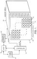
- the top level architecture of such an embodiment is depicted in Figure 1 where each Processing Element 10 is arranged on a two dimensional processor array lattice 12.
- This architecture is most easily discussed in three major groupings of functional units: the host computer 16, the controller 18, and the Processor Array 20.
- the controller unit 18 interfaces to both the host computer 16 and to the Processor Array 20.
- the controller 18 contains a microprogram memory area 32 that can be accessed by the host 16. High level programs can be written and compiled on the host 16 and the generated control information can be downloaded from the host 16 to the microprogram memory 32 of the controller 18.
- the controller 18 broadcasts an instruction and possibly a memory address to the Processor Array 20 during each processing cycle.
- the processors 10 in the Processor Array 20 perform operations received from the controller 18 based on a mask flag available in each Processing Element 10.
- the Processor Array unit 20 contains all the processing elements 10 and the supporting interconnection network 14. Each Processing Element 10 in the Processor Array 20 has direct access to its local column of memory within the architecture's memory space 23. Due to this distributed memory organization, memory conflicts are eliminated which consequently simplifies both the hardware and the software designs.
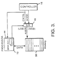
- the Processing Element 10 makes up the computational engine of the system. As mentioned above, the Processing Elements 10 are part of the Processor Array 20 subsystem and all receive the same instruction stream, but perform the required operations on their own local data stream. Each Processing Element 10 is comprised of a number of Functional Units 24, a small register file 26, interprocessor communication ports 28, s shift register (S/R) 29, and a mask flag 30 as illustrated in FIG. 2.
- each instruction word contains a specific field to control the loading and shifting of data into the memory address modifying register 29. This field is used when the memory address supplied by the instruction needs to be uniquely modified based on some local information in each processor 10, as in the case of a table lookup.
- a novel feature of a computer architecture embodying the present invention is its hardware support mechanism for implementing indirect addressing or a variable accuracy lookup table in the SIMD architecture.
- Neural network models are a practical example of the use of the present invention in a SIMD architecture.
- Such neural network models use a variety of non-linear transfer functions such as the sigmoid, the ramp, and the threshold functions. These functions can be efficiently implemented through the use of a lookup table.
- Implementation of a table lookup mechanism on a SIMD architecture requires a method for generation/modification of the memory address supplied by the controller 18, based on some local value in each Processing Element 10.
- BLITZEN A prior art architecture named BLITZEN developed by D.W. Blevins, E.W. Davis, R.A. Heaton and J.H. Rief and described in their article titled, "BLITZEN: A Highly Integrated Massively Parallel Machine," in the Journal of Parallel and Distributed Computing (1990), Vol. 8, pp 150 - 160, performs this task by logically ORing the 10 most significant bits of the memory address supplied by the controller, with a local register value.
- Such a scheme does not offer sufficient flexibility as required for general-purpose neurocomputer design.
- the accuracy, or level of quantization of the neuron output values tolerated by neural networks can vary significantly (from 2 to 16 bits) among different neural network models and different applications of each model.
- an architecture embodying the present invention incorporates two shift registers 44, 46 in FIG. 3 (shift register 44 in FIG. 3 is the equivalent of shift register 29 in FIG. 2) that are used to modify the address supplied by the controller 18.
- One shift register 44 is associated with the Processing Element 10 and keeps the data value used for addressing the lookup table.
- the other shift register 46 is associated with the Processing Element's local memory 38 and is used to modify the address received from the controller 18. See FIG. 3.
- the table lookup procedure for a table of size 2 k is initiated when the controller 18 loads the base address of the table to each of the shift registers 46 associated with each Processing Element's local memory 38 using a broadcast instruction.
- the base address value is right shifted by k bits before being broadcast by the controller 18. This will insure that the proper value is being used after the augmentation of the k bit offset value.
- the offset value is then shifted into this register 46 one bit at the time from the local register 44 in the Processing Element 10 starting from the most significant bit into the least significant bit of the memory address register 46.
- the control signals for this shifting operation are generated by the controller 18 and are broadcast to all Processing Elements 10 as part of the microinstruction word. With this procedure, an address for a table of size 2 k can be generated in k time steps by each processor. By using a bitwise shifting operation, variable accuracy can be achieved in accessing data from memory array 22.
- the present invention may be implemented by a parallel transfer into register 46 the contents of the local register 44 in the Processing Element 10.
- the advantage of the parallel shifting of data between these two registers over that of the bitwise serial shifting scheme is that only a single cycle of the architecture is needed. However, it requires more physical pins and wires for interconnection of the physical chips comprising the various functional components of the architecture and provides only a fixed accuracy into the desired table held in memory.
- bitwise shifting scheme described above has as advantages over the parallel transfer scheme that it requires only a single pinout and wire, and provides variable accuracy into the desired memory table. However, it requires more machine cycles to shift out the register contents in a bitwise fashion than the parallel transfer of the alternate scheme.
Landscapes
- Engineering & Computer Science (AREA)
- Computer Hardware Design (AREA)
- Theoretical Computer Science (AREA)
- Computing Systems (AREA)
- Physics & Mathematics (AREA)
- General Engineering & Computer Science (AREA)
- General Physics & Mathematics (AREA)
- Multi Processors (AREA)
- Executing Machine-Instructions (AREA)
- Memory System (AREA)
- Advance Control (AREA)
Applications Claiming Priority (2)
| Application Number | Priority Date | Filing Date | Title |
|---|---|---|---|
| US106343 | 1979-12-21 | ||
| US08/106,343 US5526501A (en) | 1993-08-12 | 1993-08-12 | Variable accuracy indirect addressing scheme for SIMD multi-processors and apparatus implementing same |
Publications (2)
| Publication Number | Publication Date |
|---|---|
| EP0638868A2 true EP0638868A2 (fr) | 1995-02-15 |
| EP0638868A3 EP0638868A3 (fr) | 1995-11-15 |
Family
ID=22310902
Family Applications (1)
| Application Number | Title | Priority Date | Filing Date |
|---|---|---|---|
| EP94112404A Withdrawn EP0638868A3 (fr) | 1993-08-12 | 1994-08-09 | Schéma d'adressage indirect avec précision variable pour multiprocesseurs SIMD et dispositif utilisant ce schéma. |
Country Status (5)
| Country | Link |
|---|---|
| US (1) | US5526501A (fr) |
| EP (1) | EP0638868A3 (fr) |
| JP (1) | JPH0764853A (fr) |
| CA (1) | CA2129497A1 (fr) |
| IL (1) | IL110607A0 (fr) |
Cited By (9)
| Publication number | Priority date | Publication date | Assignee | Title |
|---|---|---|---|---|
| GB2348979A (en) * | 1999-04-09 | 2000-10-18 | Pixelfusion Ltd | Parallel data processing system with shared memory |
| GB2348980A (en) * | 1999-04-09 | 2000-10-18 | Pixelfusion Ltd | Parallel data processing system with SIMD array |
| US6275928B1 (en) | 1995-07-31 | 2001-08-14 | Csem Centre Suisse D'electronique Et De Microtechnique S.A. | Microprocessor instruction pipeline having inhibit logic at each stage |
| WO2002099685A1 (fr) * | 2001-06-06 | 2002-12-12 | Afca-System Kft | Procede et circuit conçus de maniere avantageuse pour un traitement de donnees en parallele a repetition cyclique |
| DE10159283A1 (de) * | 2001-12-04 | 2003-06-12 | Systemonic Ag | Verfahren und Anordnung zur Adressgenerierung in einem Prozessor |
| WO2005017765A3 (fr) * | 2003-08-15 | 2005-04-21 | Koninkl Philips Electronics Nv | Ensemble de traitement parallele |
| US7506136B2 (en) | 1999-04-09 | 2009-03-17 | Clearspeed Technology Plc | Parallel data processing apparatus |
| US7526630B2 (en) | 1999-04-09 | 2009-04-28 | Clearspeed Technology, Plc | Parallel data processing apparatus |
| US7627736B2 (en) | 1999-04-09 | 2009-12-01 | Clearspeed Technology Plc | Thread manager to control an array of processing elements |
Families Citing this family (25)
| Publication number | Priority date | Publication date | Assignee | Title |
|---|---|---|---|---|
| JP3276782B2 (ja) * | 1994-08-18 | 2002-04-22 | 本田技研工業株式会社 | 電動補助自転車 |
| CN1120413C (zh) * | 1998-04-01 | 2003-09-03 | 北京多思科技工业园股份有限公司 | 数据相关串行操作的错位并行处理方法 |
| US6334176B1 (en) * | 1998-04-17 | 2001-12-25 | Motorola, Inc. | Method and apparatus for generating an alignment control vector |
| US6275984B1 (en) | 1998-11-20 | 2001-08-14 | Sega Of America, Inc. | System and method for delaying indirect register offset resolution |
| US7673223B2 (en) * | 2001-06-15 | 2010-03-02 | Qualcomm Incorporated | Node processors for use in parity check decoders |
| US6633856B2 (en) * | 2001-06-15 | 2003-10-14 | Flarion Technologies, Inc. | Methods and apparatus for decoding LDPC codes |
| US6938196B2 (en) * | 2001-06-15 | 2005-08-30 | Flarion Technologies, Inc. | Node processors for use in parity check decoders |
| US7681013B1 (en) * | 2001-12-31 | 2010-03-16 | Apple Inc. | Method for variable length decoding using multiple configurable look-up tables |
| US6961888B2 (en) * | 2002-08-20 | 2005-11-01 | Flarion Technologies, Inc. | Methods and apparatus for encoding LDPC codes |
| US20040157626A1 (en) * | 2003-02-10 | 2004-08-12 | Vincent Park | Paging methods and apparatus |
| US6957375B2 (en) * | 2003-02-26 | 2005-10-18 | Flarion Technologies, Inc. | Method and apparatus for performing low-density parity-check (LDPC) code operations using a multi-level permutation |
| JP4373340B2 (ja) * | 2003-02-26 | 2009-11-25 | クゥアルコム・インコーポレイテッド | 反復復号のためのソフト情報スケーリング |
| US20070234178A1 (en) * | 2003-02-26 | 2007-10-04 | Qualcomm Incorporated | Soft information scaling for interactive decoding |
| US8196000B2 (en) * | 2003-04-02 | 2012-06-05 | Qualcomm Incorporated | Methods and apparatus for interleaving in a block-coherent communication system |
| US7434145B2 (en) * | 2003-04-02 | 2008-10-07 | Qualcomm Incorporated | Extracting soft information in a block-coherent communication system |
| US7231557B2 (en) * | 2003-04-02 | 2007-06-12 | Qualcomm Incorporated | Methods and apparatus for interleaving in a block-coherent communication system |
| US7237181B2 (en) * | 2003-12-22 | 2007-06-26 | Qualcomm Incorporated | Methods and apparatus for reducing error floors in message passing decoders |
| US7346832B2 (en) * | 2004-07-21 | 2008-03-18 | Qualcomm Incorporated | LDPC encoding methods and apparatus |
| US7395490B2 (en) * | 2004-07-21 | 2008-07-01 | Qualcomm Incorporated | LDPC decoding methods and apparatus |
| US7127659B2 (en) * | 2004-08-02 | 2006-10-24 | Qualcomm Incorporated | Memory efficient LDPC decoding methods and apparatus |
| US7441099B2 (en) * | 2006-10-03 | 2008-10-21 | Hong Kong Applied Science and Technology Research Institute Company Limited | Configurable SIMD processor instruction specifying index to LUT storing information for different operation and memory location for each processing unit |
| US8112691B1 (en) * | 2008-03-25 | 2012-02-07 | Oracle America, Inc. | Method for efficient generation of a Fletcher checksum using a single SIMD pipeline |
| US8737736B2 (en) * | 2010-12-31 | 2014-05-27 | Microsoft Corporation | Tone mapping of very large aerial image mosaic |
| US9436847B2 (en) * | 2014-09-26 | 2016-09-06 | Intel Corporation | Cryptographic pointer address encoding |
| US11314674B2 (en) | 2020-02-14 | 2022-04-26 | Google Llc | Direct memory access architecture with multi-level multi-striding |
Family Cites Families (3)
| Publication number | Priority date | Publication date | Assignee | Title |
|---|---|---|---|---|
| US4065808A (en) * | 1975-01-25 | 1977-12-27 | U.S. Philips Corporation | Network computer system |
| US5129092A (en) * | 1987-06-01 | 1992-07-07 | Applied Intelligent Systems,Inc. | Linear chain of parallel processors and method of using same |
| US5212777A (en) * | 1989-11-17 | 1993-05-18 | Texas Instruments Incorporated | Multi-processor reconfigurable in single instruction multiple data (SIMD) and multiple instruction multiple data (MIMD) modes and method of operation |
-
1993
- 1993-08-12 US US08/106,343 patent/US5526501A/en not_active Expired - Lifetime
-
1994
- 1994-08-04 CA CA002129497A patent/CA2129497A1/fr not_active Abandoned
- 1994-08-09 EP EP94112404A patent/EP0638868A3/fr not_active Withdrawn
- 1994-08-09 IL IL11060794A patent/IL110607A0/xx unknown
- 1994-08-12 JP JP6190729A patent/JPH0764853A/ja active Pending
Cited By (11)
| Publication number | Priority date | Publication date | Assignee | Title |
|---|---|---|---|---|
| US6275928B1 (en) | 1995-07-31 | 2001-08-14 | Csem Centre Suisse D'electronique Et De Microtechnique S.A. | Microprocessor instruction pipeline having inhibit logic at each stage |
| GB2348979A (en) * | 1999-04-09 | 2000-10-18 | Pixelfusion Ltd | Parallel data processing system with shared memory |
| GB2348980A (en) * | 1999-04-09 | 2000-10-18 | Pixelfusion Ltd | Parallel data processing system with SIMD array |
| GB2348980B (en) * | 1999-04-09 | 2004-05-12 | Pixelfusion Ltd | Parallel data processing systems |
| US7506136B2 (en) | 1999-04-09 | 2009-03-17 | Clearspeed Technology Plc | Parallel data processing apparatus |
| US7526630B2 (en) | 1999-04-09 | 2009-04-28 | Clearspeed Technology, Plc | Parallel data processing apparatus |
| US7627736B2 (en) | 1999-04-09 | 2009-12-01 | Clearspeed Technology Plc | Thread manager to control an array of processing elements |
| WO2002099685A1 (fr) * | 2001-06-06 | 2002-12-12 | Afca-System Kft | Procede et circuit conçus de maniere avantageuse pour un traitement de donnees en parallele a repetition cyclique |
| DE10159283A1 (de) * | 2001-12-04 | 2003-06-12 | Systemonic Ag | Verfahren und Anordnung zur Adressgenerierung in einem Prozessor |
| WO2005017765A3 (fr) * | 2003-08-15 | 2005-04-21 | Koninkl Philips Electronics Nv | Ensemble de traitement parallele |
| US7725681B2 (en) | 2003-08-15 | 2010-05-25 | Nxp B.V. | Parallel processing array |
Also Published As
| Publication number | Publication date |
|---|---|
| IL110607A0 (en) | 1994-11-11 |
| US5526501A (en) | 1996-06-11 |
| EP0638868A3 (fr) | 1995-11-15 |
| JPH0764853A (ja) | 1995-03-10 |
| CA2129497A1 (fr) | 1995-02-13 |
Similar Documents
| Publication | Publication Date | Title |
|---|---|---|
| US5526501A (en) | Variable accuracy indirect addressing scheme for SIMD multi-processors and apparatus implementing same | |
| US5204938A (en) | Method of implementing a neural network on a digital computer | |
| US6219775B1 (en) | Massively parallel computer including auxiliary vector processor | |
| US5796972A (en) | Method and apparatus for performing microcode paging during instruction execution in an instruction processor | |
| US4363104A (en) | Imaging system having multiple image copying and hierarchical busing | |
| US5664214A (en) | Parallel processing computer containing a multiple instruction stream processing architecture | |
| US4314333A (en) | Data processor | |
| US5586256A (en) | Computer system using multidimensional addressing between multiple processors having independently addressable internal memory for efficient reordering and redistribution of data arrays between the processors | |
| US4974146A (en) | Array processor | |
| US4375678A (en) | Redundant memory arrangement providing simultaneous access | |
| US4218757A (en) | Device for automatic modification of ROM contents by a system selected variable | |
| JP2002509312A (ja) | 不整列データ・アクセスを実行するためのデータ整列バッファを有するディジタル信号プロセッサ | |
| US5539898A (en) | Data-array processing system wherein parallel processors access to the memory system is optimized | |
| US20110078409A1 (en) | Method and system for local memory addressing in single instruction, multiple data computer system | |
| JP3063006B2 (ja) | マイクロプログラムされるコンピュータ装置及びマイクロコードシーケンスメモリをアドレツシングする方法 | |
| US4740911A (en) | Dynamically controlled interleaving | |
| US4302809A (en) | External data store memory device | |
| US7573481B2 (en) | Method and apparatus for management of bit plane resources | |
| US5546532A (en) | Data-array processing system | |
| EP0009093B1 (fr) | Sous-système de mémoire autonome avec réallocation dynamique | |
| US5602986A (en) | Data processing and memory systems with retained background color information | |
| EP0226103A2 (fr) | Génération d'adresse pour processeurs en réseau cellulaire | |
| EP0521265A2 (fr) | Système de traitement parallèle | |
| JPS6058503B2 (ja) | デ−タ処理制御方式 | |
| JPH05290188A (ja) | 超並列計算機 |
Legal Events
| Date | Code | Title | Description |
|---|---|---|---|
| PUAI | Public reference made under article 153(3) epc to a published international application that has entered the european phase |
Free format text: ORIGINAL CODE: 0009012 |
|
| AK | Designated contracting states |
Kind code of ref document: A2 Designated state(s): BE DE ES FR GB IT NL SE |
|
| PUAL | Search report despatched |
Free format text: ORIGINAL CODE: 0009013 |
|
| AK | Designated contracting states |
Kind code of ref document: A3 Designated state(s): BE DE ES FR GB IT NL SE |
|
| STAA | Information on the status of an ep patent application or granted ep patent |
Free format text: STATUS: THE APPLICATION IS DEEMED TO BE WITHDRAWN |
|
| 18D | Application deemed to be withdrawn |
Effective date: 19960516 |