EP0638904A2 - Doppelzugriffspeicher - Google Patents
Doppelzugriffspeicher Download PDFInfo
- Publication number
- EP0638904A2 EP0638904A2 EP94410047A EP94410047A EP0638904A2 EP 0638904 A2 EP0638904 A2 EP 0638904A2 EP 94410047 A EP94410047 A EP 94410047A EP 94410047 A EP94410047 A EP 94410047A EP 0638904 A2 EP0638904 A2 EP 0638904A2
- Authority
- EP
- European Patent Office
- Prior art keywords
- output
- line
- cell
- read
- memory
- Prior art date
- Legal status (The legal status is an assumption and is not a legal conclusion. Google has not performed a legal analysis and makes no representation as to the accuracy of the status listed.)
- Granted
Links
Images


Classifications
-
- G—PHYSICS
- G11—INFORMATION STORAGE
- G11C—STATIC STORES
- G11C7/00—Arrangements for writing information into, or reading information out from, a digital store
- G11C7/10—Input/output [I/O] data interface arrangements, e.g. I/O data control circuits, I/O data buffers
- G11C7/1075—Input/output [I/O] data interface arrangements, e.g. I/O data control circuits, I/O data buffers for multiport memories each having random access ports and serial ports, e.g. video RAM
-
- G—PHYSICS
- G11—INFORMATION STORAGE
- G11C—STATIC STORES
- G11C11/00—Digital stores characterised by the use of particular electric or magnetic storage elements; Storage elements therefor
- G11C11/21—Digital stores characterised by the use of particular electric or magnetic storage elements; Storage elements therefor using electric elements
- G11C11/34—Digital stores characterised by the use of particular electric or magnetic storage elements; Storage elements therefor using electric elements using semiconductor devices
- G11C11/40—Digital stores characterised by the use of particular electric or magnetic storage elements; Storage elements therefor using electric elements using semiconductor devices using transistors
- G11C11/41—Digital stores characterised by the use of particular electric or magnetic storage elements; Storage elements therefor using electric elements using semiconductor devices using transistors forming static cells with positive feedback, i.e. cells not needing refreshing or charge regeneration, e.g. bistable multivibrator or Schmitt trigger
- G11C11/413—Auxiliary circuits, e.g. for addressing, decoding, driving, writing, sensing, timing or power reduction
- G11C11/417—Auxiliary circuits, e.g. for addressing, decoding, driving, writing, sensing, timing or power reduction for memory cells of the field-effect type
- G11C11/419—Read-write [R-W] circuits
-
- G—PHYSICS
- G11—INFORMATION STORAGE
- G11C—STATIC STORES
- G11C7/00—Arrangements for writing information into, or reading information out from, a digital store
-
- G—PHYSICS
- G11—INFORMATION STORAGE
- G11C—STATIC STORES
- G11C7/00—Arrangements for writing information into, or reading information out from, a digital store
- G11C7/10—Input/output [I/O] data interface arrangements, e.g. I/O data control circuits, I/O data buffers
- G11C7/1006—Data managing, e.g. manipulating data before writing or reading out, data bus switches or control circuits therefor
-
- G—PHYSICS
- G11—INFORMATION STORAGE
- G11C—STATIC STORES
- G11C8/00—Arrangements for selecting an address in a digital store
- G11C8/04—Arrangements for selecting an address in a digital store using a sequential addressing device, e.g. shift register, counter
-
- G—PHYSICS
- G11—INFORMATION STORAGE
- G11C—STATIC STORES
- G11C8/00—Arrangements for selecting an address in a digital store
- G11C8/16—Multiple access memory array, e.g. addressing one storage element via at least two independent addressing line groups
Definitions
- the present invention relates to dual-access memories, that is to say which comprise a separate input and output, and more particularly memories of the first-in / first-out (FIFO) type.
- dual-access memories that is to say which comprise a separate input and output, and more particularly memories of the first-in / first-out (FIFO) type.
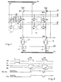
- FIG. 1 partially shows a conventional dual access memory structure.
- This memory comprises dual access memory cells 10 arranged in columns.
- each cell 10 comprises, for example, two inverters 10-1 arranged head to tail.
- Each inverter includes a pair of complementary output transistors (N and P channel MOS).
- the input and the output of the cell correspond respectively to the input and the output of a first of the inverters.
- the second inverter the output of which is connected to the input of the memory cell, includes more resistive output transistors than those of the first inverter, which limits the current consumption during a writing in the cell.
- Each column of cells is associated with an input line Bi and an output line Bo.
- the input of each cell 10 of a column is connected to the corresponding input line Bi by an N-channel MOS transistor M1.
- the output of each cell 10 of a column is connected to the corresponding output line Bo by an N channel MOS transistor M2.
- the gates of the transistors M1 of the same row of cells are connected to a writing line W and the gates of the transistors M2 of the same row of cells are connected to a reading line R.
- Each output line Bo is connected to a high supply potential Vdd by a P-channel MOS transistor MP1, called the precharge transistor.
- Each output line Bo is connected to an output Bo1 of the memory by successively an N-channel MOS transistor M3, a latch 12 consisting of inverters arranged head to tail, and a three-state gate 14.
- the transistors MP1 and M3 are controlled by a column reading signal RC.
- the three-state doors 14 are controlled by a validation signal EN which, as the case may be, is equal to the signal RC or fixed by an external device, such as a microprocessor, which reads the memory.
- the MP1 preload transistors can also be N-channel; in this case they are controlled by the logical inverse of the RC signal.
- the input lines Bi are connected directly, or via follower amplifiers not shown, to respective lines of an input data bus Di.
- the outputs Bo1 of the memory are connected to the respective lines of an output bus Do.
- data buses Di and Do of n lines, dual access memories of n columns are associated.
- the write W and read R lines are controlled by an address decoder, not shown.
- a device managing the input bus Di presents data on the bus Di, transmits an address (on an address bus not shown) which selects one of the rows of cells, and activates a line WC column writing (not shown in Figure 1).
- a device which manages the Do bus sends an address which selects one of the rows of cells, activates the line RC for reading columns, and validates the line EN.
- the dual-access memories of the type of FIG. 1 are often used in first-in / first-out (FIFO) type memories.
- a FIFO memory does not include an address bus.
- the column reading line RC is activated and the data that the memory then presents on its output (Bo1) is recovered.
- the WC column write line is activated by presenting data at its input (Bi).
- a FIFO memory generally comprises a dual access memory of the type of FIG. 1 with its address decoder, the addresses being supplied by a relatively complex control circuit which manages the "first-in / first-out" mechanism. depending on the WC read and RC column write signals, supplied from outside.
- FIG. 2 represents the appearance of various signals of the structure of FIG. 1 during the successive reading of a "0" in a first cell and twice a "1" in a second cell. At successive times t1, t2 and t3, it is decided to carry out the abovementioned readings.
- the column reading line RC and a line R1 which corresponds to one of the reading lines R are activated.
- the transistor MP2 is turned on and transmits the output of cell 10 on the output line Bo.
- the transistor MP1 is blocked and the line Bo is not forced to the potential Vdd.
- the cell 10 read stores a "0", which means that the input of the cell is at "0" while its output is at "1".
- line Bo remains at "1”.
- the transistor M3 is turned on and transmits the state "1" of the line Bo on the input of the latch 12 which reverses this state.
- the output Bo1, and the corresponding line of the bus Do pass or remain at "0".
- the lines RC and R1 are deactivated before time t2, which makes the precharge transistors MP1 conductive and blocks the output transistors M3.
- An object of the present invention is to provide a dual access memory structure having a particularly low consumption.
- Another object of the present invention is to provide a FIFO memory with particularly low consumption and of particularly simple structure.
- a dual-access memory comprising dual-access memory cells arranged in columns.
- One output line per column is connected to each cell of the column by a read transistor controlled by a respective read line.
- Precharge transistors connect the output lines to a precharge potential corresponding to a first logic state, these transistors being controlled by an inactive state of a read selection signal.
- Output transistors connect the output lines to an output of the memory.
- a false memory cell is associated with a false output line and a precharge transistor, the output of this false cell being in a second logic state opposite to said first logic state.
- a false read transistor is controlled by the active state of the read selection signal and connects the output of the false cell to the false output line. Means are provided for controlling said output transistors when the state of the false output line reaches a predetermined threshold between said first and second logic states.
- one entry line per column is connected to each cell of the column by a writing transistor controlled by a respective writing line.
- the memory includes, for each write line, a transistor connecting this write line to an input of the memory and controlled by the active state of a write select signal.
- the means for controlling the output transistors comprise a logic gate, a first input of which is connected to the false output line by means of an inverter and of which a second input receives the signal selection in reading.
- the false cell comprises a conductive transistor connected to a fixed potential corresponding to said second logic state.
- the memory is a first-in / first-out type memory comprising: a first looped shift register whose outputs respectively control the read lines, the shift of this register being controlled by the inverse of the read selection signal; and a second looped shift register, the outputs of which respectively control said write lines, the shift of this register being controlled by the inverse of the write selection signal.
- FIG. 3 the same elements as in FIG. 1 are designated by the same references.
- a false memory cell 10 ′ is provided for all of the columns of cells, the output of this false cell being connected to a false output line Bo ′ by an N channel MOS transistor M2 ′.
- the output of this false cell 10 ' is permanently fixed at "0" by an N-channel MOS transistor 10-2, connected between the transistor M2' and the ground, and the gate of which is connected to the potential Vdd.
- the transistors M2 'and 10-2 are chosen with the same characteristics, respectively, as the transistors M2 and the N-channel output transistor of a memory cell.
- the false output line Bo ' is connected to the potential Vdd, like the other output lines Bo, by a precharge transistor MP1, the gate of which is controlled by the column read signal RC. Unlike the read transistors M2, the gate of the transistor M2 'for reading the false cell is connected to the line RC.
- the gates of the output transistors M3, instead of being connected to the line RC, are connected to a line RC2 connected to the output of an AND gate 16.
- a first input of the AND gate 16 is connected to the line RC and the other to the false output line Bo 'via an inverter 18.
- FIG. 4 represents the appearance of various signals from the memory of FIG. 3 when a "1" is read in a memory cell while a "1" has previously been read in a cell of the same column. This case corresponds to the instant t3 of FIG. 2 where the output of a conventional memory presented an untimely transition to "0".
- the lines R and RC are activated.
- the preload transistors MP1 are blocked, the transistor M2 'and the transistor M2 of the cell to be read become conducting.
- the output of the false cell 10 'and the output of the cell 10 to be read are at "0", which causes, as shown, a progressive and synchronous discharge of the output lines Bo and Bo'.
- the threshold voltage Vt of the inverter 18 is not reached; the output of gate 16 remains at "0" and the output transistors M3 remain blocked.
- This first phase corresponds to the interval where the output of a conventional memory has an untimely transition to "0", as shown in dotted lines for the output Bo1.
- This inadvertent change to "0" is avoided, according to the invention, thanks to the fact that the output transistors M3 remain blocked during this first phase.
- each input line Bi is connected to the input of the memory by an N-channel MOS transistor M4.
- the gates of the M4 transistors are connected to a WC column writing line.
- the WC line is a line which is used to select the write memory; it is active at the same time as any of the writing lines W.
- FIG. 5 represents an embodiment of a circuit for controlling the write W and read R lines, making it possible, using a dual-access memory, to produce a FIFO memory of particularly simple structure.
- FIG. 5 illustrates an example where there are six reading lines R and six writing lines W.
- a circuit of the type of FIG. 5 is associated with the six reading lines R and another identical circuit is associated with the six lines writing W. We only describe below the control circuit associated with the reading lines.
- This control circuit includes a shift register with six flip-flops 20 arranged in cascade, that is to say that the output of each flip-flop is connected to the input of the next flip-flop.
- Each output of a flip-flop 20 is supplied to one of the reading lines R by an AND gate 22.
- a second input of AND doors 22 is connected to the column reading line RC which is also connected to the clock inputs of the flip-flops 20 via an inverter 24.
- a initialization signal RST is supplied to each of the flip-flops 20. Activation of this RST signal sets the first flip-flop 20 to "1" and all the others to "0".
- the shift register is looped back, that is to say that the output of the last flip-flop is connected to the input of the first flip-flop.
- the flip-flops 20 are arranged in an interlaced manner, that is to say that the flip-flop of last row (6) is disposed between the flip-flops of first row (1) and second row (2), that the penultimate penultimate row (5) is disposed between the second row (2) and third row (3) scales ...
- the connections between the scales are all of substantially the same length, whatever the number of flip-flops, which prevents the flip-flops from having different switching times.
- the flip-flop of rank 1 is at "1" and all the others at "0".
- the RC line is activated, the first row of cells is selected for reading.
- the RC line is deactivated, the "1" which was in the first flip-flop propagates in the second flip-flop.
- the second row of cells is selected for reading.
- the "1" reaches the last flip-flop (6), it returns to the first flip-flop as soon as the RC signal is deactivated.
- a control circuit identical to that of FIG. 5 is also associated with the writing lines W.
- the writing lines W are connected to the outputs of the AND gates 22 and the column writing line WC is connected to the input of the inverter 24.
- the ranks of the flip-flops can be changed if one wishes to read the stored data in an order different from that of their writing.
- a particularly simple FIFO memory structure is thus obtained since the rows of cells are directly selected by the shift registers without the need to use a conventional complex system for generating addresses and decoding these addresses.
- the devices which write or read in the FIFO memory can know the filling state of the latter. For this, these devices need a FULL signal indicating that the memory is full and possibly a 1 ⁇ 2FULL signal indicating that the memory is half full.
- FIG. 6 schematically represents a circuit making it possible to obtain such FULL and 1 ⁇ 2FULL signals.
- This circuit includes two counters per L 30 and 32, L being the number of rows of cells of the FIFO memory (6 in the example of FIG. 5).
- the counter 30 is activated by the column write line WC and the counter 32 is activated by the column read line RC.
- the two counters 30 and 32 are reset to zero by the signal RST.
- the outputs of the counters 30 and 32 are supplied to a digital subtractor 34 which provides the difference between the content of the counter 30 and that of the counter 32 (i.e. the difference between the number of written data and the number of data read).
- the output of the subtractor 34 is supplied to an input a of two comparators 36 and 38.
- An input b of the comparator 36 receives the number L-1 and an input b of the comparator 38 receives the number L / 2.
- the comparator 36 provides the full signal FULL when the result of the subtraction in the subtractor 34 is equal to L-1 and the comparator 38 activates the half-full state signal 1 ⁇ 2FULL when the result of the sub
Landscapes
- Engineering & Computer Science (AREA)
- Microelectronics & Electronic Packaging (AREA)
- Multimedia (AREA)
- Computer Hardware Design (AREA)
- Static Random-Access Memory (AREA)
Priority Applications (1)
| Application Number | Priority Date | Filing Date | Title |
|---|---|---|---|
| EP98201225A EP0863512B1 (de) | 1993-07-12 | 1994-07-08 | Doppelzugriffspeicher |
Applications Claiming Priority (2)
| Application Number | Priority Date | Filing Date | Title |
|---|---|---|---|
| FR9308837 | 1993-07-12 | ||
| FR9308837A FR2707790B1 (fr) | 1993-07-12 | 1993-07-12 | Mémoire à double accès. |
Related Child Applications (2)
| Application Number | Title | Priority Date | Filing Date |
|---|---|---|---|
| EP98201225A Division EP0863512B1 (de) | 1993-07-12 | 1994-07-08 | Doppelzugriffspeicher |
| EP98201225.4 Division-Into | 1998-04-16 |
Publications (3)
| Publication Number | Publication Date |
|---|---|
| EP0638904A2 true EP0638904A2 (de) | 1995-02-15 |
| EP0638904A3 EP0638904A3 (de) | 1995-04-12 |
| EP0638904B1 EP0638904B1 (de) | 2000-01-05 |
Family
ID=9449365
Family Applications (2)
| Application Number | Title | Priority Date | Filing Date |
|---|---|---|---|
| EP94410047A Expired - Lifetime EP0638904B1 (de) | 1993-07-12 | 1994-07-08 | Doppelzugriffspeicher |
| EP98201225A Expired - Lifetime EP0863512B1 (de) | 1993-07-12 | 1994-07-08 | Doppelzugriffspeicher |
Family Applications After (1)
| Application Number | Title | Priority Date | Filing Date |
|---|---|---|---|
| EP98201225A Expired - Lifetime EP0863512B1 (de) | 1993-07-12 | 1994-07-08 | Doppelzugriffspeicher |
Country Status (5)
| Country | Link |
|---|---|
| US (2) | US5946261A (de) |
| EP (2) | EP0638904B1 (de) |
| JP (1) | JPH07334989A (de) |
| DE (2) | DE69422453T2 (de) |
| FR (1) | FR2707790B1 (de) |
Families Citing this family (12)
| Publication number | Priority date | Publication date | Assignee | Title |
|---|---|---|---|---|
| CA2253128A1 (en) * | 1998-10-30 | 2000-04-30 | Mosaid Technologies Incorporated | Structure of random access memory formed of multibit cells |
| US6469925B1 (en) * | 2000-07-14 | 2002-10-22 | Raj Kumar Jain | Memory cell with improved retention time |
| US6546461B1 (en) | 2000-11-22 | 2003-04-08 | Integrated Device Technology, Inc. | Multi-port cache memory devices and FIFO memory devices having multi-port cache memory devices therein |
| US6768668B2 (en) * | 2001-06-12 | 2004-07-27 | Infineon Technologies Aktiengesellschaft | Converting volatile memory to non-volatile memory |
| US6741517B1 (en) * | 2002-03-29 | 2004-05-25 | Mindspeed Technologies, Inc. | Four port RAM cell |
| JP2004192694A (ja) * | 2002-12-10 | 2004-07-08 | Renesas Technology Corp | 半導体記憶装置 |
| FR2864320A1 (fr) | 2003-12-19 | 2005-06-24 | St Microelectronics Sa | Nouvelle architecture de memoire fifo et procede de gestion d'une telle memoire. |
| US7042792B2 (en) * | 2004-01-14 | 2006-05-09 | Integrated Device Technology, Inc. | Multi-port memory cells for use in FIFO applications that support data transfers between cache and supplemental memory arrays |
| US7221607B1 (en) | 2005-02-09 | 2007-05-22 | Lattice Semiconductor Corporation | Multi-port memory systems and methods for bit line coupling |
| US7145829B1 (en) | 2005-06-16 | 2006-12-05 | International Business Machines Corporation | Single cycle refresh of multi-port dynamic random access memory (DRAM) |
| JP2007018584A (ja) * | 2005-07-06 | 2007-01-25 | Matsushita Electric Ind Co Ltd | 半導体記憶装置 |
| JP4875682B2 (ja) * | 2008-09-30 | 2012-02-15 | 富士フイルム株式会社 | レンズ枠、レンズ組立体および撮影装置 |
Family Cites Families (7)
| Publication number | Priority date | Publication date | Assignee | Title |
|---|---|---|---|---|
| US4864543A (en) * | 1987-04-30 | 1989-09-05 | Texas Instruments Incorporated | First-in, first-out memory with counter address pointers for generating multiple memory status flags |
| JPS63237296A (ja) * | 1987-03-25 | 1988-10-03 | Toshiba Corp | 半導体記憶装置 |
| US5121346A (en) * | 1989-03-31 | 1992-06-09 | Sgs-Thomson Microelectronics, Inc. | Difference comparison between two asynchronous pointers and a programmable value |
| GB8923037D0 (en) * | 1989-10-12 | 1989-11-29 | Inmos Ltd | Timing control for a memory |
| KR950004453B1 (ko) * | 1990-09-07 | 1995-05-01 | 니뽄 덴끼 가부시끼가이샤 | 한 레지스터의 내용을 다른 레지스터에 카피하는 레지스터 회로 |
| JP3357382B2 (ja) * | 1991-05-28 | 2002-12-16 | 株式会社日立製作所 | 多ポートメモリ |
| JPH05151778A (ja) * | 1991-06-05 | 1993-06-18 | Mitsubishi Electric Corp | スタテイツクランダムアクセスメモリおよびその制御方法 |
-
1993
- 1993-07-12 FR FR9308837A patent/FR2707790B1/fr not_active Expired - Fee Related
-
1994
- 1994-07-08 EP EP94410047A patent/EP0638904B1/de not_active Expired - Lifetime
- 1994-07-08 DE DE69422453T patent/DE69422453T2/de not_active Expired - Fee Related
- 1994-07-08 DE DE69429374T patent/DE69429374D1/de not_active Expired - Lifetime
- 1994-07-08 EP EP98201225A patent/EP0863512B1/de not_active Expired - Lifetime
- 1994-07-11 JP JP18044994A patent/JPH07334989A/ja not_active Withdrawn
-
1996
- 1996-05-06 US US08/643,735 patent/US5946261A/en not_active Expired - Lifetime
-
1998
- 1998-04-02 US US09/053,978 patent/US6144608A/en not_active Expired - Lifetime
Also Published As
| Publication number | Publication date |
|---|---|
| DE69429374D1 (de) | 2002-01-17 |
| FR2707790B1 (fr) | 1995-09-15 |
| US5946261A (en) | 1999-08-31 |
| DE69422453D1 (de) | 2000-02-10 |
| EP0863512B1 (de) | 2001-12-05 |
| EP0638904A3 (de) | 1995-04-12 |
| EP0638904B1 (de) | 2000-01-05 |
| FR2707790A1 (fr) | 1995-01-20 |
| EP0863512A1 (de) | 1998-09-09 |
| JPH07334989A (ja) | 1995-12-22 |
| US6144608A (en) | 2000-11-07 |
| DE69422453T2 (de) | 2000-09-07 |
Similar Documents
| Publication | Publication Date | Title |
|---|---|---|
| EP3252774B1 (de) | Adaptierter speicherschaltkreis zur durchführung von rechenoperationen | |
| EP0638904B1 (de) | Doppelzugriffspeicher | |
| FR2666436A1 (fr) | Memoire a semi-conducteurs a acces rapide. | |
| US6108254A (en) | Dynamic random access memory having continuous data line equalization except at address transition during data reading | |
| FR2473814A1 (fr) | Circuit mos dynamique ne dependant pas d'un rapport de resistances destine a constituer des circuits logiques divers | |
| EP0626696A1 (de) | Dynamischer Speicher | |
| FR2475330A1 (fr) | Dispositif d'aiguillage de donnees numeriques | |
| GB2583121A (en) | In memory computation | |
| FR2718272A1 (fr) | Mémoire vive vidéo et procédé pour fournir en sortie des données série. | |
| EP0215497B1 (de) | Autokorrelationseinrichtung | |
| EP0632388B1 (de) | Prozessorsystem, insbesondere für Bildverarbeitung mit einem Speicherbus von variabler Grösse | |
| EP1027643B1 (de) | Pipelinemikroprozessor mit verarbeitung von bedingten verzweigungungen in einem einzigen taktzyklus | |
| FR2765719A1 (fr) | Perfectionnement aux memoires a acces sequentiels | |
| EP0887804B1 (de) | Leseverfahren und Schaltung für dynamischen Speicher | |
| EP0831590B1 (de) | Ausgangspufferschaltkreis für logische Signale | |
| EP0449190B1 (de) | Programmschalteinrichtung zur Erzeugung von binären Ausgangssignalen als Reaktion auf ein Taktsignal | |
| FR2683934A1 (fr) | Circuit pour augmenter la vitesse de fonctionnement d'un dispositif de memoire a semi-conducteur. | |
| FR2796224A1 (fr) | Circuit logique adiabatique | |
| FR2635600A1 (fr) | Unite de memoire adressable a circuit de selection d'unite ameliore | |
| EP0717349B1 (de) | Anordnung zur Verwaltung eines FIFO-Speichers | |
| FR2599527A1 (fr) | Ensemble de memoires dynamiques et dispositif de commande d'un tel ensemble | |
| EP1235225A2 (de) | Verfahren und Anordnung für serielle Speicherauslesung mit Adressensprung | |
| CH689959A5 (fr) | Automate insensible aux délais d'horloge. | |
| JPH06259992A (ja) | 半導体集積回路 | |
| FR2710777A1 (fr) | Dispositif électronique de mémoire à accès séquentiel. |
Legal Events
| Date | Code | Title | Description |
|---|---|---|---|
| PUAI | Public reference made under article 153(3) epc to a published international application that has entered the european phase |
Free format text: ORIGINAL CODE: 0009012 |
|
| AK | Designated contracting states |
Kind code of ref document: A2 Designated state(s): DE FR GB IT |
|
| PUAL | Search report despatched |
Free format text: ORIGINAL CODE: 0009013 |
|
| AK | Designated contracting states |
Kind code of ref document: A3 Designated state(s): DE FR GB IT |
|
| 17P | Request for examination filed |
Effective date: 19950915 |
|
| 17Q | First examination report despatched |
Effective date: 19971204 |
|
| RAP3 | Party data changed (applicant data changed or rights of an application transferred) |
Owner name: STMICROELECTRONICS S.A. |
|
| GRAG | Despatch of communication of intention to grant |
Free format text: ORIGINAL CODE: EPIDOS AGRA |
|
| GRAG | Despatch of communication of intention to grant |
Free format text: ORIGINAL CODE: EPIDOS AGRA |
|
| GRAH | Despatch of communication of intention to grant a patent |
Free format text: ORIGINAL CODE: EPIDOS IGRA |
|
| GRAH | Despatch of communication of intention to grant a patent |
Free format text: ORIGINAL CODE: EPIDOS IGRA |
|
| GRAA | (expected) grant |
Free format text: ORIGINAL CODE: 0009210 |
|
| AK | Designated contracting states |
Kind code of ref document: B1 Designated state(s): DE FR GB IT |
|
| REF | Corresponds to: |
Ref document number: 69422453 Country of ref document: DE Date of ref document: 20000210 |
|
| GBT | Gb: translation of ep patent filed (gb section 77(6)(a)/1977) |
Effective date: 20000228 |
|
| ITF | It: translation for a ep patent filed | ||
| PLBE | No opposition filed within time limit |
Free format text: ORIGINAL CODE: 0009261 |
|
| STAA | Information on the status of an ep patent application or granted ep patent |
Free format text: STATUS: NO OPPOSITION FILED WITHIN TIME LIMIT |
|
| 26N | No opposition filed | ||
| REG | Reference to a national code |
Ref country code: GB Ref legal event code: IF02 |
|
| PGFP | Annual fee paid to national office [announced via postgrant information from national office to epo] |
Ref country code: DE Payment date: 20030717 Year of fee payment: 10 |
|
| PG25 | Lapsed in a contracting state [announced via postgrant information from national office to epo] |
Ref country code: DE Free format text: LAPSE BECAUSE OF NON-PAYMENT OF DUE FEES Effective date: 20050201 |
|
| PG25 | Lapsed in a contracting state [announced via postgrant information from national office to epo] |
Ref country code: IT Free format text: LAPSE BECAUSE OF NON-PAYMENT OF DUE FEES;WARNING: LAPSES OF ITALIAN PATENTS WITH EFFECTIVE DATE BEFORE 2007 MAY HAVE OCCURRED AT ANY TIME BEFORE 2007. THE CORRECT EFFECTIVE DATE MAY BE DIFFERENT FROM THE ONE RECORDED. Effective date: 20050708 |
|
| PGFP | Annual fee paid to national office [announced via postgrant information from national office to epo] |
Ref country code: GB Payment date: 20130626 Year of fee payment: 20 |
|
| PGFP | Annual fee paid to national office [announced via postgrant information from national office to epo] |
Ref country code: FR Payment date: 20130722 Year of fee payment: 20 |
|
| REG | Reference to a national code |
Ref country code: GB Ref legal event code: PE20 Expiry date: 20140707 |
|
| PG25 | Lapsed in a contracting state [announced via postgrant information from national office to epo] |
Ref country code: GB Free format text: LAPSE BECAUSE OF EXPIRATION OF PROTECTION Effective date: 20140707 |