EP0638930A1 - Nouvelle technique d'interconnexion en TiSi2/TiN revêtu - Google Patents
Nouvelle technique d'interconnexion en TiSi2/TiN revêtu Download PDFInfo
- Publication number
- EP0638930A1 EP0638930A1 EP94100298A EP94100298A EP0638930A1 EP 0638930 A1 EP0638930 A1 EP 0638930A1 EP 94100298 A EP94100298 A EP 94100298A EP 94100298 A EP94100298 A EP 94100298A EP 0638930 A1 EP0638930 A1 EP 0638930A1
- Authority
- EP
- European Patent Office
- Prior art keywords
- tisi2
- tin
- region
- recited
- local interconnect
- Prior art date
- Legal status (The legal status is an assumption and is not a legal conclusion. Google has not performed a legal analysis and makes no representation as to the accuracy of the status listed.)
- Granted
Links
Images

Classifications
-
- H—ELECTRICITY
- H10—SEMICONDUCTOR DEVICES; ELECTRIC SOLID-STATE DEVICES NOT OTHERWISE PROVIDED FOR
- H10D—INORGANIC ELECTRIC SEMICONDUCTOR DEVICES
- H10D84/00—Integrated devices formed in or on semiconductor substrates that comprise only semiconducting layers, e.g. on Si wafers or on GaAs-on-Si wafers
- H10D84/01—Manufacture or treatment
- H10D84/0107—Integrating at least one component covered by H10D12/00 or H10D30/00 with at least one component covered by H10D8/00, H10D10/00 or H10D18/00, e.g. integrating IGFETs with BJTs
- H10D84/0109—Integrating at least one component covered by H10D12/00 or H10D30/00 with at least one component covered by H10D8/00, H10D10/00 or H10D18/00, e.g. integrating IGFETs with BJTs the at least one component covered by H10D12/00 or H10D30/00 being a MOS device
-
- H—ELECTRICITY
- H10—SEMICONDUCTOR DEVICES; ELECTRIC SOLID-STATE DEVICES NOT OTHERWISE PROVIDED FOR
- H10W—GENERIC PACKAGES, INTERCONNECTIONS, CONNECTORS OR OTHER CONSTRUCTIONAL DETAILS OF DEVICES COVERED BY CLASS H10
- H10W20/00—Interconnections in chips, wafers or substrates
- H10W20/01—Manufacture or treatment
- H10W20/031—Manufacture or treatment of conductive parts of the interconnections
- H10W20/064—Manufacture or treatment of conductive parts of the interconnections by modifying the conductivity of conductive parts, e.g. by alloying
- H10W20/066—Manufacture or treatment of conductive parts of the interconnections by modifying the conductivity of conductive parts, e.g. by alloying by forming silicides of refractory metals
-
- H—ELECTRICITY
- H10—SEMICONDUCTOR DEVICES; ELECTRIC SOLID-STATE DEVICES NOT OTHERWISE PROVIDED FOR
- H10D—INORGANIC ELECTRIC SEMICONDUCTOR DEVICES
- H10D84/00—Integrated devices formed in or on semiconductor substrates that comprise only semiconducting layers, e.g. on Si wafers or on GaAs-on-Si wafers
- H10D84/01—Manufacture or treatment
- H10D84/02—Manufacture or treatment characterised by using material-based technologies
- H10D84/03—Manufacture or treatment characterised by using material-based technologies using Group IV technology, e.g. silicon technology or silicon-carbide [SiC] technology
- H10D84/038—Manufacture or treatment characterised by using material-based technologies using Group IV technology, e.g. silicon technology or silicon-carbide [SiC] technology using silicon technology, e.g. SiGe
-
- H—ELECTRICITY
- H10—SEMICONDUCTOR DEVICES; ELECTRIC SOLID-STATE DEVICES NOT OTHERWISE PROVIDED FOR
- H10W—GENERIC PACKAGES, INTERCONNECTIONS, CONNECTORS OR OTHER CONSTRUCTIONAL DETAILS OF DEVICES COVERED BY CLASS H10
- H10W20/00—Interconnections in chips, wafers or substrates
- H10W20/01—Manufacture or treatment
- H10W20/031—Manufacture or treatment of conductive parts of the interconnections
- H10W20/0698—Local interconnections
-
- H—ELECTRICITY
- H10—SEMICONDUCTOR DEVICES; ELECTRIC SOLID-STATE DEVICES NOT OTHERWISE PROVIDED FOR
- H10W—GENERIC PACKAGES, INTERCONNECTIONS, CONNECTORS OR OTHER CONSTRUCTIONAL DETAILS OF DEVICES COVERED BY CLASS H10
- H10W20/00—Interconnections in chips, wafers or substrates
- H10W20/40—Interconnections external to wafers or substrates, e.g. back-end-of-line [BEOL] metallisations or vias connecting to gate electrodes
- H10W20/41—Interconnections external to wafers or substrates, e.g. back-end-of-line [BEOL] metallisations or vias connecting to gate electrodes characterised by their conductive parts
- H10W20/44—Conductive materials thereof
- H10W20/4403—Conductive materials thereof based on metals, e.g. alloys, metal silicides
- H10W20/4437—Conductive materials thereof based on metals, e.g. alloys, metal silicides the principal metal being a transition metal
- H10W20/4441—Conductive materials thereof based on metals, e.g. alloys, metal silicides the principal metal being a transition metal the principal metal being a refractory metal
-
- Y—GENERAL TAGGING OF NEW TECHNOLOGICAL DEVELOPMENTS; GENERAL TAGGING OF CROSS-SECTIONAL TECHNOLOGIES SPANNING OVER SEVERAL SECTIONS OF THE IPC; TECHNICAL SUBJECTS COVERED BY FORMER USPC CROSS-REFERENCE ART COLLECTIONS [XRACs] AND DIGESTS
- Y10—TECHNICAL SUBJECTS COVERED BY FORMER USPC
- Y10S—TECHNICAL SUBJECTS COVERED BY FORMER USPC CROSS-REFERENCE ART COLLECTIONS [XRACs] AND DIGESTS
- Y10S257/00—Active solid-state devices, e.g. transistors, solid-state diodes
- Y10S257/915—Active solid-state devices, e.g. transistors, solid-state diodes with titanium nitride portion or region
Definitions
- L local interconnect
- TiN has been used as an LI. However, TiN is very difficult to etch without damaging a silicide layer on a substrate.
- the original process for TiSi2 LI begins with deposition of an amorphous silicon layer onto titanium.
- the Si layer is photographically defined and etched.
- Annealing in N2 causes the remaining Si to react with the underlying Ti to form TiSi2, while exposed Ti regions react with the ambient N2 to form TiN.
- the TiN is then selectively removed with an H2SO4 + H2O2 solution.
- both contacts and LI are formed simultaneously. Because a high selectively to Ti as between Ti and Si can be achieved by dry etching in a fluorine-based chemistry, this process has an etch advantage over the standard TiN LI process, which exhibits less selectively to the salicided substrate.
- TiSi2 interconnect straps are formed by reaction of a silicon-on-titanium bilayer.
- a thin TiN layer between the silicide strap and previously salicided regions provides an effective diffusion barrier against counterdoping and substrate silicon outdiffusion.
- the excellent dry etch selectivity between Si and Ti simplifies the LI patterning process.
- the new LI structure also offers improved electrical performance over the standard TiN LI because of its lower electrical resistance.
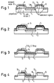
- FIGS 1 through 4 illustrate cross-sectional drawings of the in-process formation of the local interconnect according to the invention.
- Figure 5 illustrates a SEM cross-section of a TiSi2/TiN clad LI.
- the invention provides a novel TiSi2/TiN clad local interconnect technology which can be fabricated according to a double Ti deposition sequence.
- a diffusion region 4 is formed in silicon substrate 2.
- a thin oxide is grown over substrate 2 and polysilicon is deposited overall.
- the polysilicon is patterned and etched along with the oxide to form gate oxide 6 and poly gate 8 as shown.
- sidewall oxide 10 for the gates are formed by depositing a thick oxide region overall and anisotropically etching the oxide away to leave sidewall filaments.
- a conductive refractory metal such as Ti is then deposited overall.
- an anneal is performed in ambient N2 which leads to silicidation of the silicon and titanium at the silicon/titanium interfaces and leads to a first barrier metal region or layer such as TiN being formed at the surface of the exposed Ti.
- a second refractory metal layer which is conductive such as a second layer of titanium is deposited overall followed by the deposition of an amorphous silicon layer ( ⁇ -Si), resulting in a Si/Ti bilayer.
- ⁇ -Si amorphous silicon layer
- the amorphous silicon layer is then patterned and dry etched using a fluorine-based chemistry.
- annealing the structure undergoing processing in N2 leads to silicidation of the Si/Ti regions while the exposed Ti forms TiN.
- the resulting interconnect strap geometry results in a thin barrier layer such as TiN layer 12 under a conducting layer strap like TiSi2 strap 14.
- the diffusion of impurities may chemically modify the TiN layer such that it resists dissolution during the TiN wet strip process.
- the excellent adhesion between the upper level TiSi2 and the TiN layer may also provide enhanced resistance to undercutting.
- a high temperature anneal is performed to reduce the TiSi2 and TiN sheet resistivities.
- the Si/Ti reaction occurs on both Si and SiO2 substrates; since Ti will react more with Si than with SiO2, it is difficult to optimize the Si/Ti ratio.
- the Ti reaction with the substrate is prevented by the TiN barrier layer, thus Si/Ti ratio is determined by the thickness of Si and Ti within the bilayer.
- Prior art TiN LI's are fabricated from a TiN layer formed during salicidation.
- a two step wet/dry process is used to pattern the TiN LI. Although this process does not require any deposition steps other that the first Ti layer, the dry etching of TiN has poor selectivity to the substrate.
- TiSi2/TiN process not only is the excellent dry etch selectivity of the original TiSi2 process retained, but there is minimal loss of substrate from the wet etch. Because the salicided contacts are not degraded during the wet etch process, excellent contact resistance results can be achieved.
- the clad TiSi2 layer can be regarded as an electrically conductive hard mask for the wet TiN strip process.
- a comparison of typical parametric data for both TiSi2/TiN clad LI and TiN LI is shown in table 1.
- Fifty test structures were subjected to measurement and average values are indicated in table 1.
- the standard deviation (sig., short for sigma) of each set of fifty measurements is indicated within parentheses.
- 3000 LI's were constructed (referred to as an LI chain) and the ohms per strap were measured for both the TiN LI strap and the TiSi2/TiN LI strap of the invention.
- Significantly lower resistances were measured for the invention's LIs regardless of whether these straps were constructed over N+ doped diffusions (N+ chain), P+ doped diffusions (P+ chain) or over two poly regions (PLY chain).
- LI serving as resistors can be distinguished generally by their relatively long length in comparison with non-resistor LIs.
- Ohms per square measurements are indicated in table 1 for LI resistors measuring 150 ⁇ m by 0.8 ⁇ m and for LI resistors measuring 150 ⁇ m by 1.2 ⁇ m.
- a topography resistor can be constructed according to the invention by placing an LI resistor strap over a composite comprising poly moat, sidewall oxide and the like. Measurements for LI topography resistors measuring 150 ⁇ m by 0.8 ⁇ m are indicated in table 1.
- the invention's TiSi2/TiN clad process combines the advantages of both the TiSi2 and the TiN LI processes.
- the large dry etch selectivity between Si and Ti for the TiSi2 process is retained.
- the retention of a thin TiN layer between the interconnect and the contacts provides a diffusion barrier against counterdoping of phosphorous, which relaxes the thermal budget (thermal budget being a function of temperature multiplied by time) for subsequent processing (i.e., the invention allows higher temperature processing over longer times).
- the clad TiSi2 layer can be regarded as an electrically conductive hard mask for a wet TiN strip process. Improved electrical characteristics result from the intrinsically lower resistivity of TiSi2 as compared to TiN.
Landscapes
- Internal Circuitry In Semiconductor Integrated Circuit Devices (AREA)
- Electrodes Of Semiconductors (AREA)
- Metal-Oxide And Bipolar Metal-Oxide Semiconductor Integrated Circuits (AREA)
Applications Claiming Priority (2)
| Application Number | Priority Date | Filing Date | Title |
|---|---|---|---|
| US320993A | 1993-01-12 | 1993-01-12 | |
| US3209 | 1993-01-12 |
Publications (2)
| Publication Number | Publication Date |
|---|---|
| EP0638930A1 true EP0638930A1 (fr) | 1995-02-15 |
| EP0638930B1 EP0638930B1 (fr) | 2002-04-24 |
Family
ID=21704729
Family Applications (1)
| Application Number | Title | Priority Date | Filing Date |
|---|---|---|---|
| EP94100298A Expired - Lifetime EP0638930B1 (fr) | 1993-01-12 | 1994-01-11 | Nouvelle technique d'interconnexion en TiSi2/TiN revêtu |
Country Status (6)
| Country | Link |
|---|---|
| US (1) | US5936306A (fr) |
| EP (1) | EP0638930B1 (fr) |
| JP (1) | JPH077095A (fr) |
| KR (1) | KR100309857B1 (fr) |
| DE (1) | DE69430461T2 (fr) |
| TW (1) | TW270226B (fr) |
Families Citing this family (9)
| Publication number | Priority date | Publication date | Assignee | Title |
|---|---|---|---|---|
| WO1997017724A1 (fr) * | 1995-11-06 | 1997-05-15 | Seiko Epson Corporation | Dispositif a semi-conducteurs ayant une section de cablage local et son procede de fabrication |
| US6391760B1 (en) * | 1998-12-08 | 2002-05-21 | United Microelectronics Corp. | Method of fabricating local interconnect |
| US6737716B1 (en) * | 1999-01-29 | 2004-05-18 | Kabushiki Kaisha Toshiba | Semiconductor device and method of manufacturing the same |
| US6495413B2 (en) | 2001-02-28 | 2002-12-17 | Ramtron International Corporation | Structure for masking integrated capacitors of particular utility for ferroelectric memory integrated circuits |
| US6423592B1 (en) | 2001-06-26 | 2002-07-23 | Ramtron International Corporation | PZT layer as a temporary encapsulation and hard mask for a ferroelectric capacitor |
| US6534807B2 (en) | 2001-08-13 | 2003-03-18 | International Business Machines Corporation | Local interconnect junction on insulator (JOI) structure |
| US7479437B2 (en) * | 2006-04-28 | 2009-01-20 | International Business Machines Corporation | Method to reduce contact resistance on thin silicon-on-insulator device |
| KR101641347B1 (ko) | 2014-12-15 | 2016-07-21 | 피앤씨테크 주식회사 | 환기 팬 및 가스 차단기 제어 시스템 및 방법 |
| KR20230158772A (ko) | 2022-05-12 | 2023-11-21 | (주)엘엑스하우시스 | 조리 상황 인지 장치 및 방법 |
Citations (2)
| Publication number | Priority date | Publication date | Assignee | Title |
|---|---|---|---|---|
| EP0443958A1 (fr) * | 1990-02-23 | 1991-08-28 | France Telecom | Procédé de fabrication d'un circuit intégré pour filière analogique rapide utilisant des lignes d'interconnexions locales en siliciure |
| EP0517368A2 (fr) * | 1991-05-03 | 1992-12-09 | STMicroelectronics, Inc. | Interconnexion locale pour circuits intégrés |
Family Cites Families (11)
| Publication number | Priority date | Publication date | Assignee | Title |
|---|---|---|---|---|
| US3777364A (en) * | 1972-07-31 | 1973-12-11 | Fairchild Camera Instr Co | Methods for forming metal/metal silicide semiconductor device interconnect system |
| US4804636A (en) * | 1985-05-01 | 1989-02-14 | Texas Instruments Incorporated | Process for making integrated circuits having titanium nitride triple interconnect |
| US4975756A (en) * | 1985-05-01 | 1990-12-04 | Texas Instruments Incorporated | SRAM with local interconnect |
| US4814854A (en) * | 1985-05-01 | 1989-03-21 | Texas Instruments Incorporated | Integrated circuit device and process with tin-gate transistor |
| US4746219A (en) * | 1986-03-07 | 1988-05-24 | Texas Instruments Incorporated | Local interconnect |
| JPS6358943A (ja) * | 1986-08-29 | 1988-03-14 | Mitsubishi Electric Corp | 電極・配線膜の構造 |
| US4782380A (en) * | 1987-01-22 | 1988-11-01 | Advanced Micro Devices, Inc. | Multilayer interconnection for integrated circuit structure having two or more conductive metal layers |
| US4962414A (en) * | 1988-02-11 | 1990-10-09 | Sgs-Thomson Microelectronics, Inc. | Method for forming a contact VIA |
| US5168076A (en) * | 1990-01-12 | 1992-12-01 | Paradigm Technology, Inc. | Method of fabricating a high resistance polysilicon load resistor |
| US5091763A (en) * | 1990-12-19 | 1992-02-25 | Intel Corporation | Self-aligned overlap MOSFET and method of fabrication |
| US5173450A (en) * | 1991-12-30 | 1992-12-22 | Texas Instruments Incorporated | Titanium silicide local interconnect process |
-
1994
- 1994-01-11 EP EP94100298A patent/EP0638930B1/fr not_active Expired - Lifetime
- 1994-01-11 DE DE69430461T patent/DE69430461T2/de not_active Expired - Fee Related
- 1994-01-12 KR KR1019940000404A patent/KR100309857B1/ko not_active Expired - Lifetime
- 1994-01-12 JP JP6025850A patent/JPH077095A/ja active Pending
- 1994-06-08 TW TW083105195A patent/TW270226B/zh not_active IP Right Cessation
-
1995
- 1995-01-06 US US08/369,562 patent/US5936306A/en not_active Expired - Lifetime
Patent Citations (2)
| Publication number | Priority date | Publication date | Assignee | Title |
|---|---|---|---|---|
| EP0443958A1 (fr) * | 1990-02-23 | 1991-08-28 | France Telecom | Procédé de fabrication d'un circuit intégré pour filière analogique rapide utilisant des lignes d'interconnexions locales en siliciure |
| EP0517368A2 (fr) * | 1991-05-03 | 1992-12-09 | STMicroelectronics, Inc. | Interconnexion locale pour circuits intégrés |
Non-Patent Citations (1)
| Title |
|---|
| S.P.JENG ET AL.: "A NOVEL TISI2/TIN CLAD LOCAL INTERCONNECT TECHNOLOGY", SYMPOSIUM ON VLSI TECHNOLOGY 17-19 MAY 1993, KYOTO, pages 105 - 106 * |
Also Published As
| Publication number | Publication date |
|---|---|
| US5936306A (en) | 1999-08-10 |
| DE69430461D1 (de) | 2002-05-29 |
| KR940018699A (ko) | 1994-08-18 |
| KR100309857B1 (ko) | 2003-07-16 |
| TW270226B (fr) | 1996-02-11 |
| JPH077095A (ja) | 1995-01-10 |
| DE69430461T2 (de) | 2002-11-14 |
| EP0638930B1 (fr) | 2002-04-24 |
Similar Documents
| Publication | Publication Date | Title |
|---|---|---|
| US5589417A (en) | TiSi2 /TiN clad interconnect technology | |
| US4920073A (en) | Selective silicidation process using a titanium nitride protective layer | |
| US5027185A (en) | Polycide gate FET with salicide | |
| EP0517368B1 (fr) | Interconnexion locale pour circuits intégrés | |
| US6028359A (en) | Integrated circuit having amorphous silicide layer in contacts and vias and method of manufacture therefor | |
| US4948747A (en) | Method of making an integrated circuit resistor | |
| US5466638A (en) | Method of manufacturing a metal interconnect with high resistance to electromigration | |
| EP0704883A2 (fr) | Chapeau de siliciure de métal réfractaire, pour protéger les structures multicouches de polycide | |
| JPS6128232B2 (fr) | ||
| EP0463373A2 (fr) | Interconnexion locale utilisant un matériau comprenant du tungstène | |
| EP0572214B1 (fr) | Procédé de fabrication d'une structure d'interconnexion dans un circuit intégré | |
| EP0638930A1 (fr) | Nouvelle technique d'interconnexion en TiSi2/TiN revêtu | |
| US20050087815A1 (en) | Semiconductor resistance element and fabrication method thereof | |
| JP2828438B2 (ja) | 半導体素子のポリサイド層形成方法 | |
| US5595935A (en) | Method for forming interconnect in integrated circuits | |
| US5413968A (en) | Semiconductor device and manufacturing method thereof | |
| JPH11233454A (ja) | 半導体装置のコンタクト形成方法 | |
| EP0120918B1 (fr) | Structure d'interconnexion en siliciure metallique-aluminium pour circuits integres et son procede de fabrication | |
| EP0514103A1 (fr) | Procédé de fabrication d'une barrière en métal pour contacts sous-micromiques | |
| JPH01300543A (ja) | 半導体装置の製造方法 | |
| KR950003221B1 (ko) | 반도체장치 제조방법 | |
| Jeng | A Novel TiSi/sub 2/TiN Clad Local Interconnect Technology | |
| JP3189399B2 (ja) | 半導体装置の製造方法 | |
| EP0486244A1 (fr) | Méthode de fabrication de contacts à faible résistance | |
| JP3031689B2 (ja) | 半導体集積回路装置およびその製造方法 |
Legal Events
| Date | Code | Title | Description |
|---|---|---|---|
| PUAI | Public reference made under article 153(3) epc to a published international application that has entered the european phase |
Free format text: ORIGINAL CODE: 0009012 |
|
| AK | Designated contracting states |
Kind code of ref document: A1 Designated state(s): DE FR GB IT NL |
|
| K1C3 | Correction of patent application (complete document) published |
Effective date: 19950215 |
|
| 17P | Request for examination filed |
Effective date: 19950720 |
|
| 17Q | First examination report despatched |
Effective date: 19960909 |
|
| GRAG | Despatch of communication of intention to grant |
Free format text: ORIGINAL CODE: EPIDOS AGRA |
|
| GRAG | Despatch of communication of intention to grant |
Free format text: ORIGINAL CODE: EPIDOS AGRA |
|
| GRAH | Despatch of communication of intention to grant a patent |
Free format text: ORIGINAL CODE: EPIDOS IGRA |
|
| GRAH | Despatch of communication of intention to grant a patent |
Free format text: ORIGINAL CODE: EPIDOS IGRA |
|
| REG | Reference to a national code |
Ref country code: GB Ref legal event code: IF02 |
|
| GRAA | (expected) grant |
Free format text: ORIGINAL CODE: 0009210 |
|
| AK | Designated contracting states |
Kind code of ref document: B1 Designated state(s): DE FR GB IT NL |
|
| PG25 | Lapsed in a contracting state [announced via postgrant information from national office to epo] |
Ref country code: NL Free format text: LAPSE BECAUSE OF FAILURE TO SUBMIT A TRANSLATION OF THE DESCRIPTION OR TO PAY THE FEE WITHIN THE PRESCRIBED TIME-LIMIT Effective date: 20020424 |
|
| REG | Reference to a national code |
Ref country code: GB Ref legal event code: FG4D |
|
| REF | Corresponds to: |
Ref document number: 69430461 Country of ref document: DE Date of ref document: 20020529 |
|
| ET | Fr: translation filed | ||
| NLV1 | Nl: lapsed or annulled due to failure to fulfill the requirements of art. 29p and 29m of the patents act | ||
| PLBE | No opposition filed within time limit |
Free format text: ORIGINAL CODE: 0009261 |
|
| STAA | Information on the status of an ep patent application or granted ep patent |
Free format text: STATUS: NO OPPOSITION FILED WITHIN TIME LIMIT |
|
| 26N | No opposition filed |
Effective date: 20030127 |
|
| PG25 | Lapsed in a contracting state [announced via postgrant information from national office to epo] |
Ref country code: IT Free format text: LAPSE BECAUSE OF NON-PAYMENT OF DUE FEES;WARNING: LAPSES OF ITALIAN PATENTS WITH EFFECTIVE DATE BEFORE 2007 MAY HAVE OCCURRED AT ANY TIME BEFORE 2007. THE CORRECT EFFECTIVE DATE MAY BE DIFFERENT FROM THE ONE RECORDED. Effective date: 20050111 |
|
| PGFP | Annual fee paid to national office [announced via postgrant information from national office to epo] |
Ref country code: IT Payment date: 20070627 Year of fee payment: 14 |
|
| PGRI | Patent reinstated in contracting state [announced from national office to epo] |
Ref country code: IT Effective date: 20080301 |
|
| PGFP | Annual fee paid to national office [announced via postgrant information from national office to epo] |
Ref country code: FR Payment date: 20080107 Year of fee payment: 15 |
|
| PGFP | Annual fee paid to national office [announced via postgrant information from national office to epo] |
Ref country code: DE Payment date: 20090130 Year of fee payment: 16 |
|
| PGFP | Annual fee paid to national office [announced via postgrant information from national office to epo] |
Ref country code: GB Payment date: 20081211 Year of fee payment: 16 |
|
| PGRI | Patent reinstated in contracting state [announced from national office to epo] |
Ref country code: IT Effective date: 20080301 |
|
| REG | Reference to a national code |
Ref country code: FR Ref legal event code: ST Effective date: 20091030 |
|
| PG25 | Lapsed in a contracting state [announced via postgrant information from national office to epo] |
Ref country code: FR Free format text: LAPSE BECAUSE OF NON-PAYMENT OF DUE FEES Effective date: 20090202 |
|
| GBPC | Gb: european patent ceased through non-payment of renewal fee |
Effective date: 20100111 |
|
| PG25 | Lapsed in a contracting state [announced via postgrant information from national office to epo] |
Ref country code: DE Free format text: LAPSE BECAUSE OF NON-PAYMENT OF DUE FEES Effective date: 20100803 |
|
| PG25 | Lapsed in a contracting state [announced via postgrant information from national office to epo] |
Ref country code: GB Free format text: LAPSE BECAUSE OF NON-PAYMENT OF DUE FEES Effective date: 20100111 |