EP0639816A2 - Circuit intégré de réseau de traitement numérique de signal programmable par l'utilisateur - Google Patents
Circuit intégré de réseau de traitement numérique de signal programmable par l'utilisateur Download PDFInfo
- Publication number
- EP0639816A2 EP0639816A2 EP94302717A EP94302717A EP0639816A2 EP 0639816 A2 EP0639816 A2 EP 0639816A2 EP 94302717 A EP94302717 A EP 94302717A EP 94302717 A EP94302717 A EP 94302717A EP 0639816 A2 EP0639816 A2 EP 0639816A2
- Authority
- EP
- European Patent Office
- Prior art keywords
- alu
- circuits
- circuit
- analog
- digital
- Prior art date
- Legal status (The legal status is an assumption and is not a legal conclusion. Google has not performed a legal analysis and makes no representation as to the accuracy of the status listed.)
- Withdrawn
Links
Images





Classifications
-
- G—PHYSICS
- G06—COMPUTING OR CALCULATING; COUNTING
- G06J—HYBRID COMPUTING ARRANGEMENTS
- G06J1/00—Hybrid computing arrangements
Definitions
- the present invention relates to integrated circuits and, more specifically, to user-programmable integrated circuits. More particularly, the present invention relates to user-programmable mixed analog and digital integrated circuits.
- FIG. 3 is a schematic diagram of an architecture for a bus interchange which can perform a single or multibit shift operation.
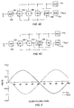
- FIG. 4b is an equivalent block diagram of the amplifier of FIG. 4a implemented according to the present invention.
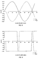
- FIG. 5 is a graph showing the waveforms of the signal input and signal output waveform of the circuit of FIG. 4b for a sinusoidal input waveform.
- FIG. 7b is an equivalent block diagram of the amplifier of FIG. 7a implemented according to the present invention in a manner which avoids pipelining distortion in the output.
- FIG. 8 is a graph showing the input and output voltages of the circuit of FIG. 7b for 1 MHz sine wave input.
- FIG. 9 is a graph showing the input and output voltages of the circuit of FIG. 7b for 1 MHz square wave input.
- FIG. 10 is a block diagram of an illustrative analog shift register configured using the architecture of the present invention.
- FIGS. 11a and 11b are examples of a series RLC tuned circuit implemented according to the present invention.
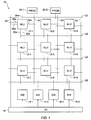
- FIG. 1 a block diagram is presented of the architecture for an illustrative field programmable digital signal processing integrated circuit according to a preferred embodiment of the present invention.
- the architecture of the present invention is integrated on a single piece of semiconductor material, and may be fabricated using known semiconductor processing technology, such as CMOS technology, which is presently preferred.
- At least one analog to digital (A/D) converter and at least one digital to analog (D/A) converter circuit may be optionally disposed on the integrated circuit along with the ALU circuits.
- A/D analog to digital
- D/A digital to analog
- FIG. 1 two A/D circuits 14-1 and 14-2 and two D/A circuits 16-1 and 16-2 are shown.
- A/D converters 14-1 and 14-2 and D/A converters 16-1 and 16-2 will probably be located near the periphery of the integrated circuit die upon which the architecture 10 of the present invention is disposed, but those of ordinary skill in the art will understand that placement of these devices is largely a matter of design choice. Such elements may even be located off chip in certain applications.
- PROM devices 20-1 and 20-2 are shown disposed in the integrated circuit architecture 10 of the present invention.
- RAM and ROM circuits may be usefully employed in the architecture of the present invention.
- a user-programmable interconnect architecture is superimposed upon the aforementioned circuit elements.
- the user-programmable interconnect architecture is used to connect the aforementioned circuit elements to one another and to the I/O pins.
- User-programmable interconnect architectures include a plurality of interconnect conductors which may be connected to one another, to inputs and outputs of the various circuit elements, and to the I/O pads by user-programmable interconnect elements.
- These user-programmable interconnect elements may take several forms as is known in the art. Examples of such elements include antifuses, of which there are numerous known examples, such as those disclosed in United States Patents Nos. 4,899,205 and 5,070,384, 5,181,096, and pass transistors, such as disclosed in the architecture described in United States Patent No. 4,870,302. Those of ordinary skill in the art will recognize that these examples are non-exhaustive and merely illustrate the state of the user-programmable interconnect element art.
- user-programmable interconnect element as used herein shall be construed to cover all forms of such interconnect elements.
- the structure, design, and use of such user-programmable interconnect elements is well known in the art and will not be recited herein.
- FIG. 1 the user-programmable interconnect architecture is shown diagrammatically as horizontal interconnect conductors 22 and vertical interconnect conductors 24 which are distributed throughout the and among the circuit elements of FIG. 1.
- FIG. 1 is very general in this respect.
- the lines identified by reference numerals 22 and 24 in the drawing figure are not intended to represent individual interconnect conductors but rather represent groups of conductors. An actual arrangement of interconnect conductors useful for employment in the present invention will be disclosed in subsequent figures and text herein.
- the interconnect conductor groups may communicate with the I/O pins, either directly, as shown in FIG. 1 by leftmost and rightmost vertical conductor groups 24 entering I/O block 18, or through appropriate input and output buffers as is known in the art.
- This feature of the present invention allows a number of integrated circuits according to the present invention to be connected together to form larger circuits, which may be clocked together as will be described further herein.
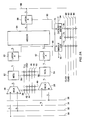
- ALU 12 includes an first 2:1 multiplexer 26 and a second 2:1 multiplexer 28. Both the first and second multiplexers 26 and 28 are n-bits wide, where n is the width of the data byte used by the ALU.
- the byte size used in any actual embodiment of the invention could be from 2-64 bits wide and will be dictated by resolution, size, and other design considerations.
- a typical byte size might be, for example, 8 bits.
- Practically a data byte would be the width of the A/D and D/A converters used. This would be for instance 8 or 10 bits in the case of Video D/A converters and 18 bits for Audio D/A converters.
- the voltage in tuned reactive circuits is Q (quality factor) times higher than the input voltage.
- Q quality factor
- a Q may be as high as 100, which would require an extra 8 bits to be added to the ALU circuits 12 to accommodate the voltage, resulting in 16 to 18 bits for Video D/A converters.
- the programmable circuit is optimized for reactive circuits, only the internal nodes of the reactive circuits need be this size. The rest of the ALU data paths could be 8 to 10 bits wide.
- ALU circuits 12 Another solution to this problem would be to configure all of the ALU circuits 12 to be 8 to 10 bits wide and to program an AGC circuit consisting of a peak detector, a comparator and gain adjust circuit into the circuit to reduce the input signal amplitude to the reactive circuit module, thereby preventing the ALU from overflowing.
- AGC circuit consisting of a peak detector, a comparator and gain adjust circuit into the circuit to reduce the input signal amplitude to the reactive circuit module, thereby preventing the ALU from overflowing.
- ALU circuit 12-1 in the region of ALU 12-1 at reference numerals 30a and 32a. While only one ALU circuit 12-1 is shown having such an input structure in FIG. 1, in order to avoid cluttering up the drawing, those of ordinary skill in the art will recognize that it is preferable for all ALU circuits to be similarly configured.
- control inputs 38 and 40 of first and second 2:1 multiplexers are brought to an interconnect matrix which includes conductor 42 carrying the VCC potential for the integrated circuit, conductor 44 carrying ground potential, and general interconnect conductors 46, 48, and 50.
- the small circles in the interconnect matrix at the intersections of control inputs 38 and 40 and conductors 42, 44, 46, 48, and 50 represent user programmable interconnect elements, such as antifuses or pass transistors.
- the outputs of negate circuits 52 and 54 drive the Latch A latches 60 and 62.
- the outputs of Latch A latches 60 and 62 form the input terms for adder 64.
- Adder 64 may be a conventional multibit adder circuit.
- the output of adder 64 drives the input of latch B 66.
- the output of Latch B 66 is connected to output bus 68.
- control circuit 70 The purpose of control circuit 70 is to synchronize the operation of the ALU to assure that the operation of the circuit is coordinated with the arrival of the correct data to be processed by the ALU.
- Control circuit 70 has a clock (CLK) input 72, an enable (EN) input 74 and an input-ready in (INRIN) input 76. These inputs are incorporated into an interconnect matrix including two clock lines CLKA line 78, CLKB line 80, and three general interconnect conductors 82, 84, and 86. The input lines are connectable to any of these lines by the user programmable interconnect elements shown as small circles at the intersections of the conductors and the input lines.
- Control circuit 70 has four outputs. Output A (line 88) drives the clocks of the Latch A Latches 62 and 62, and output B (line 90) drives the clock of the Latch B 66.
- INROUT line 92 is used for asynchronous connection of modules and is an input-read output signal which would be connected to the input-read (INRIN) input of the module connected upstream so that the upstream module will release data on the next clock.
- DATARDY line 94 is a data ready output used to indicate that data is valid for the next module downstream to read.
- FIG. 2b a state diagram is presented, showing in detail the operation of the control circuit portion of the ALU circuit of FIG. 2a.
- synchronous stages will not need to utilize the INRIN and INROUT lines.
- Asynchronous stages will use the INRIN and INROUT lines at the interface.
- Occasional bytes may be lost, but this should not affect the overall operation of any circuits configured using the architecture of the present invention. Lost bytes may be averaged out by (A+B)/2 of subsequent data bytes until smoothness level is achieved, so long as the number of data samples per cycle are adequate.
- the organization of the interconnect architecture of the present invention makes it possible to utilize the interconnect itself to perform mathematical functions such as multiply and divide.
- This feature of the present invention is advantageous in that such operations may be performed in the same clock cycle as the operations performed by the ALU whose output is driving the interconnect conductors.
- the speed will be limited by the rate at which the ALU circuits can perform an addition (subtraction) and a multiplication (division).
- the multiplication and division are the mathematical processes that take the most time. If however the application circuit is designed to use circuit elements such as resistors, capacitors inductors etc. in units of the power of 2 i.e. 2, 4, 8, 16 etc., the multiplication and division may be digitally represented by a shift left or a shift right operation.
- FIG. 3 shows a plurality of horizontal interconnect conductors 22-1 through 22-5 intersecting a plurality of vertical interconnect conductors 24-1 through 24-6. At each intersection, a transistor 56-1 through 56-36 is connected between the horizontal and vertical interconnect conductors. The gates of diagonally-situated ones of the transistors are connected together to one of gate lines 58-1 through 58-11.
- a bus interchange like that depicted in FIG. 3 may be placed at the intersection of horizontal and vertical interconnect conductors such as 22 and 24 and may also be employed to connect an input bus or output bus of an ALU to the horizontal and vertical interconnect busses of the interconnect architecture. It is apparent that the multiplication and division operations implemented by the shift function disclosed herein will take no significant time, and will certainly occur in the same clock cycle used to operate the driving ALU. Hence those of ordinary skill in the art will appreciate that the architecture of the present invention can perform functions with the same approximate speed as high speed analog operational amplifiers.
- the value of R as any power of 2 may be preprogrammed into the ALU circuit by shifting the output bus one or more bit positions. This function could be achieved in one clock cycle and the digital resistor performs the same function on each clock cycle i.e. subtract two input numbers and divide by a preprogrammed constant.
- the architecture of the present invention eliminates the need for program storage.
- the division operation for calculating capacitances whose values are powers of 2 is automatically performed as a result of a bit shift of one or more places in the opposite direction from that for a multiplication operation. Similar simple functions exist for inductors and transformers and operational amplifiers, comparators, ideal diodes, switches or multiplexers, which are the building blocks of analog electronics.
- the user-programmed interconnect of the digital ALU circuits would be a one-to-one map of the analog equivalent.
- the additional integration of digital signals is simple because the digital gates would be made of the same type of transistors for digital circuits.
- the digital modules may use similar logic as is currently available in Gate arrays, FPGA's and PAL's.
- the interconnection of the analog elements may of course be made in the same manner as used in Gate arrays, FPGA's and PAL's.
- An integrated circuit according to the present invention is easily customizable, suitable for mixing analog and digital functions, and can be extremely fast, capable of working with analog signals in the RF and Video frequency ranges.
- the limiting frequency will likely be the rate of A/D and D/A conversions at the boundaries of the system. Flash converters currently work in the tens of megahertz.
- the A/D and D/A converters could either be on chip or off chip depending on the desire of the designer/manufacturer.
- FIGS. 4a and 4b a simple design of an inverting unity gain amplifier is shown as an example of the operation of the architecture of the present invention.
- FIG. 4a is a schematic diagram of the analog equivalent circuit including two one ohm resistors, a 40 nF capacitor, and an amplifier having a slew rate of 0.25 V/V IN .
- FIG. 4b is a block diagram of the digital equivalent circuit as implemented in the architecture of the present invention.
- An analog input voltage is supplied to AID converter 100, which presents its output to ALU 102, programmed to behave as the resistor R1 in the circuit of FIG. 4a.
- ALU 104 is programmed to behave as capacitor C
- ALU 106 is programmed to behave as resistor R2
- ALU 108 is programmed to behave as the amplifier element.
- the entire circuit is driven by a 100 MHz clock 110.
- ALU 102 resistor 1
- ALU 104 capacitor C
- V1 V 1prev + (I1 + I2)(10nsec/40nF)
- V 1p is the voltage from the previous clock cycle and 10nsec is the period of the clock signal.
- FIG. 5 is a graph showing the waveforms of the signal input and signal output waveform of the circuit for a sinusoidal input waveform. It may be seen from FIG. 5 that the output of the amplifier is somewhat "phase shifted" due to the pipelining time for the data through the ALU system which emulates the analog amplifier.
- FIG. 6 is a graph showing the waveforms of the signal input and signal output waveform of the circuit of FIG. 4b for a square input waveform.
- the damped overshoot characteristic which is typical of analog amplifiers may be seen on the output waveform.
- re-arranging the architecture of the emulated amplifier circuit can eliminate the distortion exhibited by the circuit of FIG. 4b which is apparent in FIGS. 5 and 6.
- FIGS. 7a and 7b an alternate configuration can be configured by employing a slower master clock and using the data-valid (INR and OUTR ) connections of the ALU circuits.
- the same reference numerals are used in the circuits of FIGS. 4b and 7b, but the capacitor C has a value of 60nF and the amplifier has a gain of 2.
- FIGS. 8 and 9 are graphs showing the input and output voltages of the circuit of FIG. 7b for 1 MHz sine and square wave inputs, respectively.
- Those of ordinary skill in the art will recognize that, while the phase of the output voltages are lagging the input voltages, the square wave output is completely free of overshoot.
- Such skilled persons will also recognize that, due to the slower clocking speed (i.e., 33 MHz as opposed to 100MHz for the circuit of FIG. 4b), fewer data points are used to define the output function.
- the architecture of the present invention may be used to implement an analog shift register as shown in FIG. 10, thus making possible any length delay without phase alteration.
- three ALU modules 120, 122 and 124 are shown connected as an analog shift register.
- the ALU modules are configured to compute the function (V1 + 0)/1, by connecting the B input busses of each to ground and the A input busses of each module to the output bus of the preceding ALU module in the chain.
- This technique may be used to configure an analog shift register chain of arbitrary length, although only three stages are shown in FIG. 10.
- the present invention may also be employed to simulate tuned circuits.
- the actual value of the circuit element is also a function of the frequency at which the circuit is clocked. If the number that is output is the value of current, then the time period of the ALU clock signal will represent a current multiplied by time. Therefore the circuit output value is an amount of charge or Q.
- a capacitor ALU having a digital value 1, clocked at a clock frequency of 100 MHz will be a value of C/clock frequency, or 10 nanofarads.
- the actual value of the circuit elements will be set by the clock frequency of the ALU.
- One technique to avoid this problem in the circuits configured according to the present invention is to make a small FIFO of, for example, three signal bytes. This would require the use of three ALU circuits, unless the ALU circuits are optimized to perform this function.
- the load signal is determined by the output of one ALU circuit and the dump signal would be determined by the input ALU running at a different frequency. If the FIFO is, full one byte is erased and the next byte loaded. If the FIFO is empty then the last byte is kept for the next read cycle. This is of course only one of many ways to perform this function.
- Another possible method is to design the ALU circuits with hand shaking such that the waiting module will not perform any function on the next clock cycle if the adjacent module is not ready to send or receive the data.
- MIMD multiple instruction multiple data or single instruction multiple data
- SIMD multiple instruction multiple data or single instruction multiple data
- the MIMD and SIMD machines do not use interconnect to perform operations such as multiplication and division, and instead utilize the processor engines to perform these functions in the traditional manner. Nor do they utilize the concept of varying the processor clock frequency to vary the calculation result, as is employed in the present invention. Nor does any of this prior work disclose or suggest the idea of programming the interconnect to represent an analog function to run in real time. Also the processors in these arrays are very complex and are therefore stuck with the Von Neuman bottleneck is an undesirable characteristic thereof.
- the architecture of the present invention by its very nature requires each adder/shifter to perform only the one single function so there is no data bottle neck. THis provides a significant advantage over the prior art.
- Another advantage of modeling an analog circuit with an array of adders and shifters with programmable interconnect is that general integer arithmetic can be easily performed by combining adder/shifters. Hence the end user can design his device to multiply or divide a value by any integer when necessary. Since analog circuits typically move a signal along a circuit path with few feedback terms the additional time required for the integer arithmetic may not slow down the circuit as this architecture will basically pipeline the calculation so long as the calculation is not in a high speed feedback term.
- the architecture of the present invention could be implemented in an FPGA but the modules in these devices are small and designed for logic functions, typically one bit wide. Hence many modules would have to be used to make a 10 bit adder and the interconnect architectures in FPGA devices do not provide a sufficient number of lines to efficiently implement the shift function in the interconnect. Hence the circuit cost per analog function will be high and the speed will be much slower. Additionally the modules in an FPGA are not designed to accept signals arriving asynchronously with the clock signal.
- Circuits that utilize feedback that is running at the signal frequency represent the limiting frequency of the performance of this invention. This is caused by a phase shift between the signal and the reaction to that signal which represents at best one clock delay. For these applications the circuit will be more stable if the modules are clocked in series rather than in parallel. This of course causes the maximum operating frequency of the circuit to be limited (divided) by a factor of the number of series clock pulse used. Such a clocking scheme is useful for such applications for the Z transform for the specific circuit to be solved and applied to the module array as opposed to the just placing the circuit elements one to each module.
- FIGS. 11a and 11b Two examples of a simple series RLC tuned circuit implemented using the architecture of the present are shown in FIGS. 11a and 11b.
- the circuit is envisioned as an input node impressed with a voltage V in in series with an inductance L in series with a resistance R in series with a capacitance C to ground.
- ALU module 130 driven by CLK1, computes V in -V 2prev , where V 2prev is the voltage at the node joining the inductance L and resistance R at the last clock cycle.
- ALU module 132 driven by CLK2, computes i prev + ⁇ i, where i prev is the current through the RLC circuit at the previous clock cycle and ⁇ i is the change in current to the current clock cycle.
- the current is obtained by dividing the output of ALU module 130 by L (as noted in FIG. 11a). As taught herein, this may be done by the bit shifting technique disclosed with reference to FIG. 3 and accompanying disclosure.
- ALU module 134 driven by CLK3, computes V1 prev + i/C, where V1 prev is the voltage at the node connecting the resistance R to the capacitance C at the previous clock cycle and i/C is simply the current i (output of ALU module 132 divided by the capacitance C (as noted in FIG. 11a) by the bit shifting technique.
- ALU module 136 driven by CLK4, computes V1 + iR, where V1 is the voltage at the node connecting the resistance R to the capacitance C at the current clock cycle and iR is simply the current i (output of ALU module 132 multiplied by the resistance R (as noted in FIG. 11a) by the bit shifting technique.
- FIG. 11b judicious placement of the Z transform reduces the number of clocks to two and increases the number of ALU modules to five.
- the implementation of FIG. 11b doubles the maximum frequency. In this sense the present invention can be imagined as a parallel programmable Z transform.
- ALU module 148 driven by CLK1, computes V c , the voltage across the capacitance in the present cycle, as V cprev , the voltage across the capacitance C in the previous cycle, minus the quantity I prev /C.
- IR at one input to ALU module 142 may be obtained by the bit shifting techniques taught herein.
- I prev /C of ALU module 148 and I prev /LC at the input to ALU module 144 may be similarly obtained. While this bit shifting multiply and divide technique does allow use of a minimal number of ALU modules, those of ordinary skill in the art will recognize that the values of the multiplicands and divisors are limited to integers which are powers of 2, i.e., 2... 4... 8... 16 etc. Such skilled persons will recognize that divider and multiplier circuits may be configured from multiple Alu modules to provide more flexibility of component value choices at the expense of greater circuit complexity and ALU utilization.
- Variations in gain for circuits such as AGC circuits can be implemented as powers of two by designing the module interconnect with transistors that can be switched in the circuit, as opposed to hard wired interconnect with antifuses. Another method of varying gain would be to provide a resistor divider programmed into the modules wherein the resistor value is set in SRAM memory in the module that can be changed on the fly.
- this technology can combine analog and digital functions with ease.
- An example would be the combining of a digital phase locked loop to generate the various clock frequencies required to run the different circuit blocks. This would reduce the need to input these signals from off chip and therefore increase speed and reduce pin count and power consumption.
- Another feature of this architecture is that once the signal is digitized a more complex system can be built by merely adding more chips. These would be designed such the all the digital outputs for a signal are adjacent and would match up to the inputs of another chip, allowing communicating pins from to chips to be placed side by side. Lead lengths and capacitance loading are therefore minimized, allowing communication of the signal from one chip to the next at the maximum possible frequency.
- the signal need not be converted back to analog until necessary to return the signal to the real world (i.e. speaker or video monitor). Of course if the information goes to a computer then the signal need never be converted back to analog.
- the modules may be designed with gated inputs to control the time a signal is loaded as is the case in synchronizing a signal or to steer the input as is the case with multiplexers.
- this architecture could integrate integer divide and multiply in the modules to perform the calculations thereby eliminating the requirement of using component values of a power of two. Clock frequencies would not therefore need to be fractionally different. This of course would lower the speed and density of the chip but it will still be considerably faster the conventional DSP chips as there still would be no Von Neuman bottleneck.
- Some chips could be specialized by designing more specialized modules, optimized for special applications.
- a module could be optimized for the series RLC circuit example disclosed herein and could speed up the maximum chip operating frequency by about a factor of two.
Landscapes
- Engineering & Computer Science (AREA)
- Physics & Mathematics (AREA)
- Theoretical Computer Science (AREA)
- Computer Hardware Design (AREA)
- Mathematical Physics (AREA)
- Automation & Control Theory (AREA)
- Evolutionary Computation (AREA)
- Fuzzy Systems (AREA)
- General Physics & Mathematics (AREA)
- Software Systems (AREA)
- Logic Circuits (AREA)
- Analogue/Digital Conversion (AREA)
Applications Claiming Priority (2)
| Application Number | Priority Date | Filing Date | Title |
|---|---|---|---|
| US08/109,727 US5457644A (en) | 1993-08-20 | 1993-08-20 | Field programmable digital signal processing array integrated circuit |
| US109727 | 1993-08-20 |
Publications (2)
| Publication Number | Publication Date |
|---|---|
| EP0639816A2 true EP0639816A2 (fr) | 1995-02-22 |
| EP0639816A3 EP0639816A3 (fr) | 1995-11-29 |
Family
ID=22329232
Family Applications (1)
| Application Number | Title | Priority Date | Filing Date |
|---|---|---|---|
| EP94302717A Withdrawn EP0639816A3 (fr) | 1993-08-20 | 1994-04-18 | Circuit intégré de réseau de traitement numérique de signal programmable par l'utilisateur. |
Country Status (3)
| Country | Link |
|---|---|
| US (2) | US5457644A (fr) |
| EP (1) | EP0639816A3 (fr) |
| JP (1) | JPH0786921A (fr) |
Cited By (28)
| Publication number | Priority date | Publication date | Assignee | Title |
|---|---|---|---|---|
| EP1220108A3 (fr) * | 2000-10-26 | 2005-01-12 | Cypress Semiconductor Corporation | Circuit programmable |
| WO2004053716A3 (fr) * | 2002-12-12 | 2005-03-17 | Koninkl Philips Electronics Nv | Reseau de processeur programmable par l'utilisateur integre synchronise par le flux de donnees |
| US7774190B1 (en) | 2001-11-19 | 2010-08-10 | Cypress Semiconductor Corporation | Sleep and stall in an in-circuit emulation system |
| US7893724B2 (en) | 2004-03-25 | 2011-02-22 | Cypress Semiconductor Corporation | Method and circuit for rapid alignment of signals |
| US8040266B2 (en) | 2007-04-17 | 2011-10-18 | Cypress Semiconductor Corporation | Programmable sigma-delta analog-to-digital converter |
| US8069428B1 (en) | 2001-10-24 | 2011-11-29 | Cypress Semiconductor Corporation | Techniques for generating microcontroller configuration information |
| US8069436B2 (en) | 2004-08-13 | 2011-11-29 | Cypress Semiconductor Corporation | Providing hardware independence to automate code generation of processing device firmware |
| US8078970B1 (en) | 2001-11-09 | 2011-12-13 | Cypress Semiconductor Corporation | Graphical user interface with user-selectable list-box |
| US8085067B1 (en) | 2005-12-21 | 2011-12-27 | Cypress Semiconductor Corporation | Differential-to-single ended signal converter circuit and method |
| US8089461B2 (en) | 2005-06-23 | 2012-01-03 | Cypress Semiconductor Corporation | Touch wake for electronic devices |
| US8120408B1 (en) | 2005-05-05 | 2012-02-21 | Cypress Semiconductor Corporation | Voltage controlled oscillator delay cell and method |
| US8149048B1 (en) | 2000-10-26 | 2012-04-03 | Cypress Semiconductor Corporation | Apparatus and method for programmable power management in a programmable analog circuit block |
| US8160864B1 (en) | 2000-10-26 | 2012-04-17 | Cypress Semiconductor Corporation | In-circuit emulator and pod synchronized boot |
| US8176296B2 (en) | 2000-10-26 | 2012-05-08 | Cypress Semiconductor Corporation | Programmable microcontroller architecture |
| US8286125B2 (en) | 2004-08-13 | 2012-10-09 | Cypress Semiconductor Corporation | Model for a hardware device-independent method of defining embedded firmware for programmable systems |
| US8365122B2 (en) | 2007-04-30 | 2013-01-29 | Innovations Holdings, L.L.C. | Method and apparatus for configurable systems |
| US8402313B1 (en) | 2002-05-01 | 2013-03-19 | Cypress Semiconductor Corporation | Reconfigurable testing system and method |
| US8476928B1 (en) | 2007-04-17 | 2013-07-02 | Cypress Semiconductor Corporation | System level interconnect with programmable switching |
| US8499270B1 (en) | 2007-04-25 | 2013-07-30 | Cypress Semiconductor Corporation | Configuration of programmable IC design elements |
| US8516025B2 (en) | 2007-04-17 | 2013-08-20 | Cypress Semiconductor Corporation | Clock driven dynamic datapath chaining |
| US8533677B1 (en) | 2001-11-19 | 2013-09-10 | Cypress Semiconductor Corporation | Graphical user interface for dynamically reconfiguring a programmable device |
| US8717042B1 (en) | 2006-03-27 | 2014-05-06 | Cypress Semiconductor Corporation | Input/output multiplexer bus |
| US8909960B1 (en) | 2007-04-25 | 2014-12-09 | Cypress Semiconductor Corporation | Power management architecture, method and configuration system |
| US9448964B2 (en) | 2009-05-04 | 2016-09-20 | Cypress Semiconductor Corporation | Autonomous control in a programmable system |
| US9564902B2 (en) | 2007-04-17 | 2017-02-07 | Cypress Semiconductor Corporation | Dynamically configurable and re-configurable data path |
| US9720805B1 (en) | 2007-04-25 | 2017-08-01 | Cypress Semiconductor Corporation | System and method for controlling a target device |
| US9843327B1 (en) | 2000-10-26 | 2017-12-12 | Cypress Semiconductor Corporation | PSOC architecture |
| US10698662B2 (en) | 2001-11-15 | 2020-06-30 | Cypress Semiconductor Corporation | System providing automatic source code generation for personalization and parameterization of user modules |
Families Citing this family (139)
| Publication number | Priority date | Publication date | Assignee | Title |
|---|---|---|---|---|
| US6272465B1 (en) | 1994-11-02 | 2001-08-07 | Legerity, Inc. | Monolithic PC audio circuit |
| US5761099A (en) * | 1994-11-04 | 1998-06-02 | Altera Corporation | Programmable logic array integrated circuits with enhanced carry routing |
| JP2738338B2 (ja) * | 1995-04-24 | 1998-04-08 | 日本電気株式会社 | フォールトトレラントシステム |
| US5943242A (en) | 1995-11-17 | 1999-08-24 | Pact Gmbh | Dynamically reconfigurable data processing system |
| US7266725B2 (en) | 2001-09-03 | 2007-09-04 | Pact Xpp Technologies Ag | Method for debugging reconfigurable architectures |
| US5956518A (en) | 1996-04-11 | 1999-09-21 | Massachusetts Institute Of Technology | Intermediate-grain reconfigurable processing device |
| US6144327A (en) * | 1996-08-15 | 2000-11-07 | Intellectual Property Development Associates Of Connecticut, Inc. | Programmably interconnected programmable devices |
| DE19651075A1 (de) | 1996-12-09 | 1998-06-10 | Pact Inf Tech Gmbh | Einheit zur Verarbeitung von numerischen und logischen Operationen, zum Einsatz in Prozessoren (CPU's), Mehrrechnersystemen, Datenflußprozessoren (DFP's), digitalen Signal Prozessoren (DSP's) oder dergleichen |
| DE19654593A1 (de) * | 1996-12-20 | 1998-07-02 | Pact Inf Tech Gmbh | Umkonfigurierungs-Verfahren für programmierbare Bausteine zur Laufzeit |
| US6338106B1 (en) | 1996-12-20 | 2002-01-08 | Pact Gmbh | I/O and memory bus system for DFPS and units with two or multi-dimensional programmable cell architectures |
| DE19654595A1 (de) | 1996-12-20 | 1998-07-02 | Pact Inf Tech Gmbh | I0- und Speicherbussystem für DFPs sowie Bausteinen mit zwei- oder mehrdimensionaler programmierbaren Zellstrukturen |
| ATE243390T1 (de) * | 1996-12-27 | 2003-07-15 | Pact Inf Tech Gmbh | Verfahren zum selbständigen dynamischen umladen von datenflussprozessoren (dfps) sowie bausteinen mit zwei- oder mehrdimensionalen programmierbaren zellstrukturen (fpgas, dpgas, o.dgl.) |
| DE19654846A1 (de) * | 1996-12-27 | 1998-07-09 | Pact Inf Tech Gmbh | Verfahren zum selbständigen dynamischen Umladen von Datenflußprozessoren (DFPs) sowie Bausteinen mit zwei- oder mehrdimensionalen programmierbaren Zellstrukturen (FPGAs, DPGAs, o. dgl.) |
| EP0858168A1 (fr) | 1997-01-29 | 1998-08-12 | Hewlett-Packard Company | Matrice de processeur à réseau de portes programmables |
| US5959466A (en) | 1997-01-31 | 1999-09-28 | Actel Corporation | Field programmable gate array with mask programmed input and output buffers |
| DE19704044A1 (de) * | 1997-02-04 | 1998-08-13 | Pact Inf Tech Gmbh | Verfahren zur automatischen Adressgenerierung von Bausteinen innerhalb Clustern aus einer Vielzahl dieser Bausteine |
| US6542998B1 (en) | 1997-02-08 | 2003-04-01 | Pact Gmbh | Method of self-synchronization of configurable elements of a programmable module |
| DE19704728A1 (de) | 1997-02-08 | 1998-08-13 | Pact Inf Tech Gmbh | Verfahren zur Selbstsynchronisation von konfigurierbaren Elementen eines programmierbaren Bausteines |
| DE19704742A1 (de) | 1997-02-11 | 1998-09-24 | Pact Inf Tech Gmbh | Internes Bussystem für DFPs, sowie Bausteinen mit zwei- oder mehrdimensionalen programmierbaren Zellstrukturen, zur Bewältigung großer Datenmengen mit hohem Vernetzungsaufwand |
| US6150837A (en) * | 1997-02-28 | 2000-11-21 | Actel Corporation | Enhanced field programmable gate array |
| US6047115A (en) * | 1997-05-29 | 2000-04-04 | Xilinx, Inc. | Method for configuring FPGA memory planes for virtual hardware computation |
| US6421817B1 (en) | 1997-05-29 | 2002-07-16 | Xilinx, Inc. | System and method of computation in a programmable logic device using virtual instructions |
| JP3000961B2 (ja) * | 1997-06-06 | 2000-01-17 | 日本電気株式会社 | 半導体集積回路 |
| US8686549B2 (en) | 2001-09-03 | 2014-04-01 | Martin Vorbach | Reconfigurable elements |
| DE69841256D1 (de) | 1997-12-17 | 2009-12-10 | Panasonic Corp | Befehlsmaskierung um Befehlsströme einem Prozessor zuzuleiten |
| DE69834942T2 (de) | 1997-12-17 | 2007-06-06 | Panasonic Europe Ltd., Uxbridge | Vorrichtung zum Multiplizieren |
| DE69827589T2 (de) * | 1997-12-17 | 2005-11-03 | Elixent Ltd. | Konfigurierbare Verarbeitungsanordnung und Verfahren zur Benutzung dieser Anordnung, um eine Zentraleinheit aufzubauen |
| DE19861088A1 (de) | 1997-12-22 | 2000-02-10 | Pact Inf Tech Gmbh | Verfahren zur Reparatur von integrierten Schaltkreisen |
| DE19807872A1 (de) | 1998-02-25 | 1999-08-26 | Pact Inf Tech Gmbh | Verfahren zur Verwaltung von Konfigurationsdaten in Datenflußprozessoren sowie Bausteinen mit zwei- oder mehrdimensionalen programmierbaren Zellstruktur (FPGAs, DPGAs, o. dgl. |
| JP3721888B2 (ja) * | 1998-12-04 | 2005-11-30 | セイコーエプソン株式会社 | 携帯用電子機器および携帯用電子機器の制御方法 |
| US7003660B2 (en) | 2000-06-13 | 2006-02-21 | Pact Xpp Technologies Ag | Pipeline configuration unit protocols and communication |
| US6557092B1 (en) | 1999-03-29 | 2003-04-29 | Greg S. Callen | Programmable ALU |
| WO2000062421A1 (fr) * | 1999-04-14 | 2000-10-19 | Nokia Networks Oy | Filtre numerique et procede d'execution d'une multiplication sur la base d'une table de consultation |
| US6732126B1 (en) * | 1999-05-07 | 2004-05-04 | Intel Corporation | High performance datapath unit for behavioral data transmission and reception |
| CA2372364A1 (fr) * | 1999-05-07 | 2000-11-16 | Stephen L. Wasson | Appareil et procede pour circuits arithmetiques de trajet de donnees programmables |
| DE10081643D2 (de) | 1999-06-10 | 2002-05-29 | Pact Inf Tech Gmbh | Sequenz-Partitionierung auf Zellstrukturen |
| US6246258B1 (en) * | 1999-06-21 | 2001-06-12 | Xilinx, Inc. | Realizing analog-to-digital converter on a digital programmable integrated circuit |
| US7119576B1 (en) | 2000-09-18 | 2006-10-10 | Altera Corporation | Devices and methods with programmable logic and digital signal processing regions |
| US7346644B1 (en) | 2000-09-18 | 2008-03-18 | Altera Corporation | Devices and methods with programmable logic and digital signal processing regions |
| US9626325B2 (en) * | 2000-10-06 | 2017-04-18 | Pact Xpp Technologies Ag | Array processor having a segmented bus system |
| US8058899B2 (en) | 2000-10-06 | 2011-11-15 | Martin Vorbach | Logic cell array and bus system |
| AU2002220600A1 (en) | 2000-10-06 | 2002-04-15 | Pact Informationstechnologie Gmbh | Cell system with segmented intermediate cell structure |
| US7024653B1 (en) * | 2000-10-30 | 2006-04-04 | Cypress Semiconductor Corporation | Architecture for efficient implementation of serial data communication functions on a programmable logic device (PLD) |
| US6990555B2 (en) | 2001-01-09 | 2006-01-24 | Pact Xpp Technologies Ag | Method of hierarchical caching of configuration data having dataflow processors and modules having two- or multidimensional programmable cell structure (FPGAs, DPGAs, etc.) |
| US7581076B2 (en) | 2001-03-05 | 2009-08-25 | Pact Xpp Technologies Ag | Methods and devices for treating and/or processing data |
| US9037807B2 (en) | 2001-03-05 | 2015-05-19 | Pact Xpp Technologies Ag | Processor arrangement on a chip including data processing, memory, and interface elements |
| US7210129B2 (en) | 2001-08-16 | 2007-04-24 | Pact Xpp Technologies Ag | Method for translating programs for reconfigurable architectures |
| US7444531B2 (en) | 2001-03-05 | 2008-10-28 | Pact Xpp Technologies Ag | Methods and devices for treating and processing data |
| US7844796B2 (en) | 2001-03-05 | 2010-11-30 | Martin Vorbach | Data processing device and method |
| TWI234737B (en) * | 2001-05-24 | 2005-06-21 | Ip Flex Inc | Integrated circuit device |
| WO2002103532A2 (fr) | 2001-06-20 | 2002-12-27 | Pact Xpp Technologies Ag | Procede de traitement de donnees |
| US6996702B2 (en) * | 2001-07-31 | 2006-02-07 | Wis Technologies, Inc. | Processing unit with cross-coupled ALUs/accumulators and input data feedback structure including constant generator and bypass to reduce memory contention |
| US6981073B2 (en) * | 2001-07-31 | 2005-12-27 | Wis Technologies, Inc. | Multiple channel data bus control for video processing |
| US6970509B2 (en) * | 2001-07-31 | 2005-11-29 | Wis Technologies, Inc. | Cell array and method of multiresolution motion estimation and compensation |
| US7142251B2 (en) * | 2001-07-31 | 2006-11-28 | Micronas Usa, Inc. | Video input processor in multi-format video compression system |
| US7219173B2 (en) * | 2001-07-31 | 2007-05-15 | Micronas Usa, Inc. | System for video processing control and scheduling wherein commands are unaffected by signal interrupts and schedule commands are transmitted at precise time |
| US20050207663A1 (en) * | 2001-07-31 | 2005-09-22 | Weimin Zeng | Searching method and system for best matching motion vector |
| US7184101B2 (en) * | 2001-07-31 | 2007-02-27 | Micronas Usa, Inc. | Address generation for video processing |
| US7085320B2 (en) | 2001-07-31 | 2006-08-01 | Wis Technologies, Inc. | Multiple format video compression |
| US7035332B2 (en) | 2001-07-31 | 2006-04-25 | Wis Technologies, Inc. | DCT/IDCT with minimum multiplication |
| US7996827B2 (en) | 2001-08-16 | 2011-08-09 | Martin Vorbach | Method for the translation of programs for reconfigurable architectures |
| US7434191B2 (en) | 2001-09-03 | 2008-10-07 | Pact Xpp Technologies Ag | Router |
| US8686475B2 (en) | 2001-09-19 | 2014-04-01 | Pact Xpp Technologies Ag | Reconfigurable elements |
| US7577822B2 (en) | 2001-12-14 | 2009-08-18 | Pact Xpp Technologies Ag | Parallel task operation in processor and reconfigurable coprocessor configured based on information in link list including termination information for synchronization |
| US6650141B2 (en) * | 2001-12-14 | 2003-11-18 | Lattice Semiconductor Corporation | High speed interface for a programmable interconnect circuit |
| AU2003208266A1 (en) | 2002-01-19 | 2003-07-30 | Pact Xpp Technologies Ag | Reconfigurable processor |
| US7506328B2 (en) * | 2002-02-11 | 2009-03-17 | Xerox Corporation | Method and system for optimizing performance of an apparatus |
| WO2003071432A2 (fr) | 2002-02-18 | 2003-08-28 | Pact Xpp Technologies Ag | Systemes de bus et procede de reconfiguration |
| US8914590B2 (en) | 2002-08-07 | 2014-12-16 | Pact Xpp Technologies Ag | Data processing method and device |
| JP3934493B2 (ja) * | 2002-06-28 | 2007-06-20 | 富士通株式会社 | 集積回路及びシステム開発方法 |
| AU2003286131A1 (en) | 2002-08-07 | 2004-03-19 | Pact Xpp Technologies Ag | Method and device for processing data |
| US7657861B2 (en) | 2002-08-07 | 2010-02-02 | Pact Xpp Technologies Ag | Method and device for processing data |
| GB0218359D0 (en) * | 2002-08-08 | 2002-09-18 | Anadigm Ltd | Semiconductor Devices |
| WO2004038599A1 (fr) | 2002-09-06 | 2004-05-06 | Pact Xpp Technologies Ag | Structure de sequenceur reconfigurable |
| US20040242261A1 (en) * | 2003-05-29 | 2004-12-02 | General Dynamics Decision Systems, Inc. | Software-defined radio |
| US7157934B2 (en) * | 2003-08-19 | 2007-01-02 | Cornell Research Foundation, Inc. | Programmable asynchronous pipeline arrays |
| JP4700611B2 (ja) | 2003-08-28 | 2011-06-15 | ペーアーツェーテー イクスペーペー テクノロジーズ アクチエンゲゼルシャフト | データ処理装置およびデータ処理方法 |
| US7502390B2 (en) * | 2003-10-30 | 2009-03-10 | Lsi Corporation | Optimized interleaver and/or deinterleaver design |
| CN100485656C (zh) * | 2004-02-12 | 2009-05-06 | Nxp股份有限公司 | 数字信号处理集成电路及执行信号处理操作的方法 |
| US8620980B1 (en) | 2005-09-27 | 2013-12-31 | Altera Corporation | Programmable device with specialized multiplier blocks |
| WO2007082730A1 (fr) | 2006-01-18 | 2007-07-26 | Pact Xpp Technologies Ag | Procédé de définition de matériels |
| US8266198B2 (en) | 2006-02-09 | 2012-09-11 | Altera Corporation | Specialized processing block for programmable logic device |
| US8041759B1 (en) | 2006-02-09 | 2011-10-18 | Altera Corporation | Specialized processing block for programmable logic device |
| US8266199B2 (en) | 2006-02-09 | 2012-09-11 | Altera Corporation | Specialized processing block for programmable logic device |
| US8301681B1 (en) | 2006-02-09 | 2012-10-30 | Altera Corporation | Specialized processing block for programmable logic device |
| US7836117B1 (en) | 2006-04-07 | 2010-11-16 | Altera Corporation | Specialized processing block for programmable logic device |
| US7822799B1 (en) | 2006-06-26 | 2010-10-26 | Altera Corporation | Adder-rounder circuitry for specialized processing block in programmable logic device |
| US8386550B1 (en) | 2006-09-20 | 2013-02-26 | Altera Corporation | Method for configuring a finite impulse response filter in a programmable logic device |
| US7930336B2 (en) | 2006-12-05 | 2011-04-19 | Altera Corporation | Large multiplier for programmable logic device |
| US8386553B1 (en) | 2006-12-05 | 2013-02-26 | Altera Corporation | Large multiplier for programmable logic device |
| US7814137B1 (en) | 2007-01-09 | 2010-10-12 | Altera Corporation | Combined interpolation and decimation filter for programmable logic device |
| US8650231B1 (en) | 2007-01-22 | 2014-02-11 | Altera Corporation | Configuring floating point operations in a programmable device |
| US7865541B1 (en) | 2007-01-22 | 2011-01-04 | Altera Corporation | Configuring floating point operations in a programmable logic device |
| US8645450B1 (en) | 2007-03-02 | 2014-02-04 | Altera Corporation | Multiplier-accumulator circuitry and methods |
| US7949699B1 (en) | 2007-08-30 | 2011-05-24 | Altera Corporation | Implementation of decimation filter in integrated circuit device using ram-based data storage |
| US8959137B1 (en) | 2008-02-20 | 2015-02-17 | Altera Corporation | Implementing large multipliers in a programmable integrated circuit device |
| US8244789B1 (en) | 2008-03-14 | 2012-08-14 | Altera Corporation | Normalization of floating point operations in a programmable integrated circuit device |
| US8626815B1 (en) | 2008-07-14 | 2014-01-07 | Altera Corporation | Configuring a programmable integrated circuit device to perform matrix multiplication |
| US8438522B1 (en) | 2008-09-24 | 2013-05-07 | Iowa State University Research Foundation, Inc. | Logic element architecture for generic logic chains in programmable devices |
| US8661394B1 (en) | 2008-09-24 | 2014-02-25 | Iowa State University Research Foundation, Inc. | Depth-optimal mapping of logic chains in reconfigurable fabrics |
| US8255448B1 (en) | 2008-10-02 | 2012-08-28 | Altera Corporation | Implementing division in a programmable integrated circuit device |
| US8307023B1 (en) | 2008-10-10 | 2012-11-06 | Altera Corporation | DSP block for implementing large multiplier on a programmable integrated circuit device |
| US8706790B1 (en) | 2009-03-03 | 2014-04-22 | Altera Corporation | Implementing mixed-precision floating-point operations in a programmable integrated circuit device |
| US8645449B1 (en) | 2009-03-03 | 2014-02-04 | Altera Corporation | Combined floating point adder and subtractor |
| US8468192B1 (en) | 2009-03-03 | 2013-06-18 | Altera Corporation | Implementing multipliers in a programmable integrated circuit device |
| US8805916B2 (en) | 2009-03-03 | 2014-08-12 | Altera Corporation | Digital signal processing circuitry with redundancy and bidirectional data paths |
| US8886696B1 (en) | 2009-03-03 | 2014-11-11 | Altera Corporation | Digital signal processing circuitry with redundancy and ability to support larger multipliers |
| US8549055B2 (en) | 2009-03-03 | 2013-10-01 | Altera Corporation | Modular digital signal processing circuitry with optionally usable, dedicated connections between modules of the circuitry |
| US8650236B1 (en) | 2009-08-04 | 2014-02-11 | Altera Corporation | High-rate interpolation or decimation filter in integrated circuit device |
| US8396914B1 (en) | 2009-09-11 | 2013-03-12 | Altera Corporation | Matrix decomposition in an integrated circuit device |
| US8412756B1 (en) | 2009-09-11 | 2013-04-02 | Altera Corporation | Multi-operand floating point operations in a programmable integrated circuit device |
| US7948267B1 (en) | 2010-02-09 | 2011-05-24 | Altera Corporation | Efficient rounding circuits and methods in configurable integrated circuit devices |
| US8539016B1 (en) | 2010-02-09 | 2013-09-17 | Altera Corporation | QR decomposition in an integrated circuit device |
| US8601044B2 (en) | 2010-03-02 | 2013-12-03 | Altera Corporation | Discrete Fourier Transform in an integrated circuit device |
| US8458243B1 (en) | 2010-03-03 | 2013-06-04 | Altera Corporation | Digital signal processing circuit blocks with support for systolic finite-impulse-response digital filtering |
| US8484265B1 (en) | 2010-03-04 | 2013-07-09 | Altera Corporation | Angular range reduction in an integrated circuit device |
| US8510354B1 (en) | 2010-03-12 | 2013-08-13 | Altera Corporation | Calculation of trigonometric functions in an integrated circuit device |
| US8539014B2 (en) | 2010-03-25 | 2013-09-17 | Altera Corporation | Solving linear matrices in an integrated circuit device |
| US8862650B2 (en) | 2010-06-25 | 2014-10-14 | Altera Corporation | Calculation of trigonometric functions in an integrated circuit device |
| US8589463B2 (en) | 2010-06-25 | 2013-11-19 | Altera Corporation | Calculation of trigonometric functions in an integrated circuit device |
| US8577951B1 (en) | 2010-08-19 | 2013-11-05 | Altera Corporation | Matrix operations in an integrated circuit device |
| KR101359717B1 (ko) * | 2010-11-08 | 2014-02-07 | 한국전자통신연구원 | 에너지 타일 프로세서 |
| US8645451B2 (en) | 2011-03-10 | 2014-02-04 | Altera Corporation | Double-clocked specialized processing block in an integrated circuit device |
| US9600278B1 (en) | 2011-05-09 | 2017-03-21 | Altera Corporation | Programmable device using fixed and configurable logic to implement recursive trees |
| US8812576B1 (en) | 2011-09-12 | 2014-08-19 | Altera Corporation | QR decomposition in an integrated circuit device |
| US8949298B1 (en) | 2011-09-16 | 2015-02-03 | Altera Corporation | Computing floating-point polynomials in an integrated circuit device |
| US9053045B1 (en) | 2011-09-16 | 2015-06-09 | Altera Corporation | Computing floating-point polynomials in an integrated circuit device |
| US8762443B1 (en) | 2011-11-15 | 2014-06-24 | Altera Corporation | Matrix operations in an integrated circuit device |
| US8543634B1 (en) | 2012-03-30 | 2013-09-24 | Altera Corporation | Specialized processing block for programmable integrated circuit device |
| US9098332B1 (en) | 2012-06-01 | 2015-08-04 | Altera Corporation | Specialized processing block with fixed- and floating-point structures |
| US8996600B1 (en) | 2012-08-03 | 2015-03-31 | Altera Corporation | Specialized processing block for implementing floating-point multiplier with subnormal operation support |
| US9207909B1 (en) | 2012-11-26 | 2015-12-08 | Altera Corporation | Polynomial calculations optimized for programmable integrated circuit device structures |
| US9189200B1 (en) | 2013-03-14 | 2015-11-17 | Altera Corporation | Multiple-precision processing block in a programmable integrated circuit device |
| US9348795B1 (en) | 2013-07-03 | 2016-05-24 | Altera Corporation | Programmable device using fixed and configurable logic to implement floating-point rounding |
| US9250313B2 (en) * | 2013-12-04 | 2016-02-02 | Raytheon Company | Electronically reconfigurable bandwidth and channel number analog-to-digital converter circuit for radar systems |
| US9379687B1 (en) | 2014-01-14 | 2016-06-28 | Altera Corporation | Pipelined systolic finite impulse response filter |
| US9684488B2 (en) | 2015-03-26 | 2017-06-20 | Altera Corporation | Combined adder and pre-adder for high-radix multiplier circuit |
| US10942706B2 (en) | 2017-05-05 | 2021-03-09 | Intel Corporation | Implementation of floating-point trigonometric functions in an integrated circuit device |
| US11144497B2 (en) * | 2018-08-16 | 2021-10-12 | Tachyum Ltd. | System and method of populating an instruction word |
Family Cites Families (7)
| Publication number | Priority date | Publication date | Assignee | Title |
|---|---|---|---|---|
| US4870302A (en) * | 1984-03-12 | 1989-09-26 | Xilinx, Inc. | Configurable electrical circuit having configurable logic elements and configurable interconnects |
| US4718057A (en) * | 1985-08-30 | 1988-01-05 | Advanced Micro Devices, Inc. | Streamlined digital signal processor |
| US4952934A (en) * | 1989-01-25 | 1990-08-28 | Sgs-Thomson Microelectronics S.R.L. | Field programmable logic and analogic integrated circuit |
| US5200751A (en) * | 1989-06-26 | 1993-04-06 | Dallas Semiconductor Corp. | Digital to analog converter using a programmable logic array |
| US5231588A (en) * | 1989-08-15 | 1993-07-27 | Advanced Micro Devices, Inc. | Programmable gate array with logic cells having symmetrical input/output structures |
| US5107146A (en) * | 1991-02-13 | 1992-04-21 | Actel Corporation | Mixed mode analog/digital programmable interconnect architecture |
| US5191242A (en) * | 1991-05-17 | 1993-03-02 | Advanced Micro Devices, Inc. | Programmable logic device incorporating digital-to-analog converter |
-
1993
- 1993-08-20 US US08/109,727 patent/US5457644A/en not_active Ceased
-
1994
- 1994-04-18 EP EP94302717A patent/EP0639816A3/fr not_active Withdrawn
- 1994-05-19 JP JP6129711A patent/JPH0786921A/ja active Pending
-
1997
- 1997-10-08 US US08/946,928 patent/USRE37048E1/en not_active Expired - Lifetime
Cited By (36)
| Publication number | Priority date | Publication date | Assignee | Title |
|---|---|---|---|---|
| US8555032B2 (en) | 2000-10-26 | 2013-10-08 | Cypress Semiconductor Corporation | Microcontroller programmable system on a chip with programmable interconnect |
| US8160864B1 (en) | 2000-10-26 | 2012-04-17 | Cypress Semiconductor Corporation | In-circuit emulator and pod synchronized boot |
| US9843327B1 (en) | 2000-10-26 | 2017-12-12 | Cypress Semiconductor Corporation | PSOC architecture |
| US9766650B2 (en) | 2000-10-26 | 2017-09-19 | Cypress Semiconductor Corporation | Microcontroller programmable system on a chip with programmable interconnect |
| US10261932B2 (en) | 2000-10-26 | 2019-04-16 | Cypress Semiconductor Corporation | Microcontroller programmable system on a chip |
| US8176296B2 (en) | 2000-10-26 | 2012-05-08 | Cypress Semiconductor Corporation | Programmable microcontroller architecture |
| US10248604B2 (en) | 2000-10-26 | 2019-04-02 | Cypress Semiconductor Corporation | Microcontroller programmable system on a chip |
| US8149048B1 (en) | 2000-10-26 | 2012-04-03 | Cypress Semiconductor Corporation | Apparatus and method for programmable power management in a programmable analog circuit block |
| US10020810B2 (en) | 2000-10-26 | 2018-07-10 | Cypress Semiconductor Corporation | PSoC architecture |
| US10725954B2 (en) | 2000-10-26 | 2020-07-28 | Monterey Research, Llc | Microcontroller programmable system on a chip |
| EP1220108A3 (fr) * | 2000-10-26 | 2005-01-12 | Cypress Semiconductor Corporation | Circuit programmable |
| US10466980B2 (en) | 2001-10-24 | 2019-11-05 | Cypress Semiconductor Corporation | Techniques for generating microcontroller configuration information |
| US8793635B1 (en) | 2001-10-24 | 2014-07-29 | Cypress Semiconductor Corporation | Techniques for generating microcontroller configuration information |
| US8069428B1 (en) | 2001-10-24 | 2011-11-29 | Cypress Semiconductor Corporation | Techniques for generating microcontroller configuration information |
| US8078970B1 (en) | 2001-11-09 | 2011-12-13 | Cypress Semiconductor Corporation | Graphical user interface with user-selectable list-box |
| US10698662B2 (en) | 2001-11-15 | 2020-06-30 | Cypress Semiconductor Corporation | System providing automatic source code generation for personalization and parameterization of user modules |
| US8533677B1 (en) | 2001-11-19 | 2013-09-10 | Cypress Semiconductor Corporation | Graphical user interface for dynamically reconfiguring a programmable device |
| US7774190B1 (en) | 2001-11-19 | 2010-08-10 | Cypress Semiconductor Corporation | Sleep and stall in an in-circuit emulation system |
| US8402313B1 (en) | 2002-05-01 | 2013-03-19 | Cypress Semiconductor Corporation | Reconfigurable testing system and method |
| WO2004053716A3 (fr) * | 2002-12-12 | 2005-03-17 | Koninkl Philips Electronics Nv | Reseau de processeur programmable par l'utilisateur integre synchronise par le flux de donnees |
| US7893724B2 (en) | 2004-03-25 | 2011-02-22 | Cypress Semiconductor Corporation | Method and circuit for rapid alignment of signals |
| US8286125B2 (en) | 2004-08-13 | 2012-10-09 | Cypress Semiconductor Corporation | Model for a hardware device-independent method of defining embedded firmware for programmable systems |
| US8069436B2 (en) | 2004-08-13 | 2011-11-29 | Cypress Semiconductor Corporation | Providing hardware independence to automate code generation of processing device firmware |
| US8120408B1 (en) | 2005-05-05 | 2012-02-21 | Cypress Semiconductor Corporation | Voltage controlled oscillator delay cell and method |
| US8089461B2 (en) | 2005-06-23 | 2012-01-03 | Cypress Semiconductor Corporation | Touch wake for electronic devices |
| US8085067B1 (en) | 2005-12-21 | 2011-12-27 | Cypress Semiconductor Corporation | Differential-to-single ended signal converter circuit and method |
| US8717042B1 (en) | 2006-03-27 | 2014-05-06 | Cypress Semiconductor Corporation | Input/output multiplexer bus |
| US8516025B2 (en) | 2007-04-17 | 2013-08-20 | Cypress Semiconductor Corporation | Clock driven dynamic datapath chaining |
| US8040266B2 (en) | 2007-04-17 | 2011-10-18 | Cypress Semiconductor Corporation | Programmable sigma-delta analog-to-digital converter |
| US9564902B2 (en) | 2007-04-17 | 2017-02-07 | Cypress Semiconductor Corporation | Dynamically configurable and re-configurable data path |
| US8476928B1 (en) | 2007-04-17 | 2013-07-02 | Cypress Semiconductor Corporation | System level interconnect with programmable switching |
| US8499270B1 (en) | 2007-04-25 | 2013-07-30 | Cypress Semiconductor Corporation | Configuration of programmable IC design elements |
| US9720805B1 (en) | 2007-04-25 | 2017-08-01 | Cypress Semiconductor Corporation | System and method for controlling a target device |
| US8909960B1 (en) | 2007-04-25 | 2014-12-09 | Cypress Semiconductor Corporation | Power management architecture, method and configuration system |
| US8365122B2 (en) | 2007-04-30 | 2013-01-29 | Innovations Holdings, L.L.C. | Method and apparatus for configurable systems |
| US9448964B2 (en) | 2009-05-04 | 2016-09-20 | Cypress Semiconductor Corporation | Autonomous control in a programmable system |
Also Published As
| Publication number | Publication date |
|---|---|
| EP0639816A3 (fr) | 1995-11-29 |
| USRE37048E1 (en) | 2001-02-06 |
| US5457644A (en) | 1995-10-10 |
| JPH0786921A (ja) | 1995-03-31 |
Similar Documents
| Publication | Publication Date | Title |
|---|---|---|
| US5457644A (en) | Field programmable digital signal processing array integrated circuit | |
| US5136188A (en) | Input/output macrocell for programmable logic device | |
| US9621173B1 (en) | Circuits and methods of implementing time-average-frequency direct period synthesizer on programmable logic chip and driving applications using the same | |
| US6034540A (en) | Programmable logic integrated circuit architecture incorporating a lonely register | |
| US7567997B2 (en) | Applications of cascading DSP slices | |
| US6512395B1 (en) | Configurable memory for programmable logic circuits | |
| US7346644B1 (en) | Devices and methods with programmable logic and digital signal processing regions | |
| US6989689B2 (en) | Interconnection and input/output resources for programmable logic integrated circuit devices | |
| US8674723B2 (en) | User registers implemented with routing circuits in a configurable IC | |
| EP0456399A2 (fr) | Module logique composé de blocs configurables combinatoires et séquentiels | |
| Payne | Asynchronous FPGA architectures | |
| US9564902B2 (en) | Dynamically configurable and re-configurable data path | |
| US6067615A (en) | Reconfigurable processor for executing successive function sequences in a processor operation | |
| US6480045B2 (en) | Digital frequency multiplier | |
| JPH0256114A (ja) | プログラマブル配線を介して結合されるアレイブロックを有するプログラマブル論理デバイス | |
| WO1994006210A1 (fr) | Elaboration de circuits integres a puces multiples utilisant le multiplexage temporel | |
| GB2312067A (en) | Programmable logic with lonely register | |
| JPH09153789A (ja) | 圧縮された構成ビット・ストリームを使用してゲート・アレイをプログラムするプログラム可能論理回路、及びその方法 | |
| US9287868B1 (en) | Logic cell for programmable logic device | |
| US20080263319A1 (en) | Universal digital block with integrated arithmetic logic unit | |
| US4965472A (en) | Programmable high speed state machine with sequencing capabilities | |
| JP2888512B2 (ja) | エミュレーション装置 | |
| JP4246200B2 (ja) | プログラマブル論理デバイス | |
| US7489162B1 (en) | Users registers in a reconfigurable IC | |
| US7613760B1 (en) | Efficient implementation of multi-channel integrators and differentiators in a programmable device |
Legal Events
| Date | Code | Title | Description |
|---|---|---|---|
| PUAI | Public reference made under article 153(3) epc to a published international application that has entered the european phase |
Free format text: ORIGINAL CODE: 0009012 |
|
| AK | Designated contracting states |
Kind code of ref document: A2 Designated state(s): DE FR GB IT |
|
| PUAL | Search report despatched |
Free format text: ORIGINAL CODE: 0009013 |
|
| AK | Designated contracting states |
Kind code of ref document: A3 Designated state(s): DE FR GB IT |
|
| 17P | Request for examination filed |
Effective date: 19960129 |
|
| STAA | Information on the status of an ep patent application or granted ep patent |
Free format text: STATUS: THE APPLICATION HAS BEEN WITHDRAWN |
|
| 18W | Application withdrawn |
Withdrawal date: 19970619 |