EP0639903A2 - Système de transmission - Google Patents
Système de transmission Download PDFInfo
- Publication number
- EP0639903A2 EP0639903A2 EP94202276A EP94202276A EP0639903A2 EP 0639903 A2 EP0639903 A2 EP 0639903A2 EP 94202276 A EP94202276 A EP 94202276A EP 94202276 A EP94202276 A EP 94202276A EP 0639903 A2 EP0639903 A2 EP 0639903A2
- Authority
- EP
- European Patent Office
- Prior art keywords
- signal
- transport unit
- address generator
- data
- phase shift
- Prior art date
- Legal status (The legal status is an assumption and is not a legal conclusion. Google has not performed a legal analysis and makes no representation as to the accuracy of the status listed.)
- Withdrawn
Links
Images


Classifications
-
- H—ELECTRICITY
- H04—ELECTRIC COMMUNICATION TECHNIQUE
- H04J—MULTIPLEX COMMUNICATION
- H04J3/00—Time-division multiplex systems
- H04J3/02—Details
- H04J3/06—Synchronising arrangements
- H04J3/07—Synchronising arrangements using pulse stuffing for systems with different or fluctuating information rates or bit rates
- H04J3/076—Bit and byte stuffing, e.g. SDH/PDH desynchronisers, bit-leaking
Definitions
- Such a transmission system can transmit a synchronous or plesiochronous signal.
- a signal that is transmitted in a plesiochronous transmission system can, for example, contain several low bit rate signals in one or more higher bit rate signals (for example 64 * 2,048 Mbit / s signals in a 139.264 Mbit / s signal).
- Such low bit rate signals are inserted in transport units as part of the plesiochronous signal.
- a synchronous transmission system which can be a system of synchronous digital hierarchy or the American system SONET (Synchronous Optical Network)
- the joining, splitting, branching, feeding or rerouting of any signal bundle is made possible.
- the plesiochronous useful channel signal streams arriving in a network node of the synchronous digital hierarchy in Europe: 2.048 Mbit / s, 34.368 Mbit / s and 139.264 Mbit / s
- STM-1 frames Long synchronous transport frames
- the STM-1 signal is structured by frame and, in addition to the actual useful data of the signal, has control information and stuffing data.
- An STM-1 frame consists of 270 columns and 9 rows (270 bytes per row).
- a container is understood to mean the basic packaging unit for digital useful signals.
- an administrative unit (“Administrative Unit") AU-4 with a container C-4 for a bit rate of 139.264 Mbit / s can be incorporated in an STM-1 frame.
- Can continue three management units AU-3 can be accommodated in the STM-1 frame.
- z. B. a management unit AU-3 a container C-3 for a bit rate of 44.736 Mbit / s.
- the second administration unit AU-3 can contain, for example, 7 "tributary unit groups" TUG-2, each with a container C-2 for a bit rate of 6.312 Mbit / s. 7 TUG-2 with 3 containers C-12 each for a bit rate of 2.048 Mbit / s can also be inserted in the third administration unit AU-3. Additional transport units (VC-4, VC-3, TU-3, TU-2, TU-12 and TU-11) are formed from the containers by adding control information and stuffing information.
- a synchronous transmission system usually contains hierarchically structured network or system levels (e.g. local network level or long-distance network level). Each network level includes synchronous digital devices.
- the clock supply of the individual synchronous digital devices is ensured by respectively assigned clock supply devices.
- This synchronization of the clock signal of the secondary clock supply device with the STM-1 signal is not possible if e.g. a private network operator only has a plesiochronous 2.048 Mbit / s signal inserted in the STM-1 signal. Then this 2.048 Mbit / s signal must be used for synchronization.
- the additional phase shift which, as mentioned above, is caused by changing an AU pointer (when shifting a VC-3 or V-4) or a TU pointer (when shifting a VC-2, VC-12 or VC-11) must be taken into account during desynchronization.
- Such desynchronization can be carried out, for example, with the desynchronizer known from EP-A2-0 435 384.
- This contains at least one buffer memory for a plesiochronous signal to be obtained from the STM-1 signal.
- the write operation in the buffer memory is carried out by a write address generator (write counter), which is controlled by a control arrangement (comparison and counter arrangement) and receives a write clock signal from a circuit for clock recovery.
- the reading process is carried out by a reading address generator (reading counter) which receives a reading clock signal from a combination of an actuator, a sigma-delta modulator and a controller.
- the differential values of the read and write addresses which are formed in a differential arrangement, are fed to the controller.
- the invention is therefore based on the object of providing a transmission system in which a phase shift in the desynchronized signal which is not caused by delay time shifts can be almost completely reversed.
- the task is solved by a transmission system of the type mentioned at the beginning that the control arrangement for determining the displacement of at least one transport unit in the signal and for delivering the determined displacement to a correction circuit is provided, which is used to form the phase shifts between a subordinate transport unit and a superordinate transport unit, and that a combination circuit in each case for combining one from the subtraction of the two phase shifts formed correction value and a difference value of the differential arrangement is provided.
- a phase shift in a higher-level transport unit VC-4 which is indicated by an AU pointer value
- a lower-level transport unit for example transport unit VC -12 or transport unit for a 2.048 Mbit / s signal
- the correction value is composed on the one hand of the calculated phase shift of the subordinate transport unit and on the other hand of the calculated phase shift of the superordinate transport unit (eg transport unit VC-4).
- phase shift of the subordinate transport unit is subtracted from the phase shift of the superordinate transport unit.
- the respective phase shifts result from evaluating the pointer bytes (for example, extracting the TU or AU pointer values from the pointer bytes).
- the phase shift is also obtained by evaluating the stuffing information in the pointer bytes.
- the phase shift in the transport units of signals in a plesiochronous transmission system results from the respective stuff bits.
- the pointer values (for example AU-4 and TU-12 pointer value) are evaluated in each case .
- the pointer values determine when, for example, a data byte of a transport unit for the 2.048 Mbit / s signal appears in the synchronous signal (e.g. STM-1 signal).
- the buffer fill level is obtained.
- the average buffer fill level can be used in an STM-1 signal for the subordinate transport units VC-2, VC-12 or VC-11 or a plesiochronous signal transported in these virtual containers to form the average phase shift.
- the phase shift of a higher-level transport unit VC-4 or VC-3 is obtained by multiplying the associated weighted AU pointer value by the STM-1 frame duration (125 ⁇ s) and dividing it.
- the number of data bytes of a higher-level transport unit VC-4 or VC-3 is determined by the multiplication result divided.
- the AU pointer value is weighted 3 for an AU-4 and 1 for an AU-3.
- the average phase shift of a transport unit VC-2, VC-12, VC-11 or a plesiochronous signal is calculated by multiplying the average buffer level by another factor.
- the factor is obtained by dividing the product of the number of data bytes of an STM-1 frame and the number of data bytes of the transport unit VC-2, VC-12, VC-11 or the plesiochronous signal by the STM-1 frame duration .
- the correction circuit can either calculate each correction value currently or contain a memory table which is provided for receiving pointer values as addresses and for delivering stored correction values.
- a memory table which is provided for receiving pointer values as addresses and for delivering stored correction values.
- the circuit for generating a read clock signal which contains at least one controller and an actuator and, together with the read address generator and the differential arrangement, forms a control loop, also for averaging the differential values or the signals derived therefrom.
- this circuit operates with a lower reading clock frequency (undersampling)
- a circuit for forming the mean value of the difference values over approximately one frame of the synchronous signal or a multiple thereof should be provided to avoid frame structure influences between the differential arrangement and the combination circuit.
- the control arrangement is provided for determining the displacement of at least one transport unit in the signal and for delivering the determined displacement to a correction circuit which is used to form the phase deviation between a subordinate transport unit and a superordinate transport unit. Furthermore, a combination circuit is provided in each case for combining a correction value formed from the subtraction of the two phase deviations and a difference value of the difference arrangement.
- a synchronous transmission system with several synchronous digital devices 1 to 4, which process signals of the synchronous digital hierarchy.
- a plurality of plesiochronous 2.048 Mbit / s signals are supplied to the device 1 designed as a synchronizer, which signals are inserted in the synchronizer 1 into an STM-1 signal which is supplied to a further synchronous digital device 2.
- the bytes of a plesiochronous 2.048 Mbit / s signal are each fitted into virtual containers VC-12 (cf. CCITT recommendation G.709).
- VC-12 virtual containers
- fixed and variable stuffing bytes are inserted.
- the variable stuffing bytes are used for phase or frequency adjustment.
- a "tributary unit" TU-12 is formed from a virtual container VC-12.
- a TU-12 has a further four additional bytes V1 to V4 compared to a VC-12.
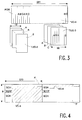
- the structure of a TU-12 is shown schematically in FIG.
- the V bytes are separated by 35 data bytes.
- the pointer value is contained in bytes V1 and V2, which indicates the beginning of a VC-12.
- the beginning of a VC-12 in a TU-12 is identified by the V5 byte.
- the V3 byte allows negative stuffing.
- a TU-12 is transported in four consecutive STM-1 frames. Therefore, the duration for the transmission of a TU-12 is 500 ⁇ s.
- the bytes of a TU-12 are stored in columns in a TUG-2.
- the 4 columns (each 9 bytes) of 3 TU-12 are alternately combined in a TUG-2 and seven TUG-2 are combined to form a VC-3 or a TUG-3.
- This nesting is shown in FIG.
- Each TUG-2 contains 12 columns (each column contains 9 bytes), which are alternately housed in a TUG-3 or VC-3.
- a TUG-3 which contains 86 columns (each 9 bytes), has fixed stuff bytes in the first column and bytes of the TU-12 transport unit in the remaining columns.
- FIG. 3 further shows, the bytes of three TUG-3 are inserted into one VC-4.
- the VC-4 contains a "Path Overhead” (POH) in the first column and fixed stuffing bytes in the following two columns. From column 4, columns of the 3 TUG-3 are inserted alternately.
- POH Path Overhead
- An STM-1 frame consists of 270 columns and 9 rows (270 bytes per row).
- the first 9 columns in lines 1 to 3 and 5 to 9 contain the "Section Overhead” (SOH) and in line 4 the "AU Pointer” (AU-P).
- SOH "Section Overhead”
- AU-P "AU Pointer"
- P the remaining area
- user data bytes, stuff bytes and other bytes for control information are inserted.
- the AU pointer AU-P contains the information about the first bit of a virtual container VC-4 or VC-3, stuffing information and other control information.
- a clock adjustment takes place in the device 2 (FIG. 1).
- a tamping process is carried out, which causes the virtual container VC-4 to move and the AU pointer value to change.
- the device 3 can fade out and fade in 2.048 Mbit / s signals.
- a clock adjustment is also carried out here. If the TU-12 pointer value is changed, this causes a stuffing process (clock adaptation with TU-12 pointer bytes).
- a 2.048 Mbit / s signal is now to be recovered in the device 4 designed as a desynchronizer.
- the STM-1 signal is resolved in the desynchronizer 4 and a plesiochronous 2.048 Mbit / s signal is formed.
- a pointer value In order to determine the beginning of a virtual container in an administration unit AU-4 or AU-3 or "tributary unit" TU-2, TU-12 or TU-11, a pointer value must be evaluated. It has been shown that phase shifts caused by stuffing between the original and the signal to be obtained cannot be completely reversed if the desynchronizer 4 is constructed according to the prior art.
- an STM-1 frame formed by the synchronizer 1 is shown above, which contains a total of 63 * VC-12 in a VC-4.
- the first, second, third and fourth columns of the VC-12 are separated by a vertical line.
- An exemplary location of TU pointer bytes (TU pointer) is also shown.
- a specific channel or column of a VC-12 is each with a small dash featured.
- the desynchronizer 4 receives the STM-1 frame shown below in the respective figures.
- the frame received in the desynchronizer 4 according to FIG. 5 only has a phase shift of 18 STM-1 bytes at 2430 STM-1 bytes of the STM-1 frame (frame duration: 125 ⁇ s) caused by runtime shifts:
- phase shift is based on the VC-12 bytes (35 bytes per STM-1 frame), the average phase shift is:
- the 0.26 bytes VC-12 represent the average phase shift or the buffer fill level for the respective transport unit VC-12.
- the STM-1 signal received in the desynchronizer has the AU-4 pointer value 6 (18 byte shift).
- the mean phase shift related to the VC-12 bytes is (see above calculation) ⁇ 0.26 VC-12 bytes ( ⁇ 0.93 ⁇ s). However, the correct mean phase shift is obtained by referring to the VC-4 bytes. This is 18 VC-4 bytes:
- the phase shift is not corrected in the desynchronization to form a 2.048 Mbit / s signal.
- the phase shift caused by changing a VC-4 or VC-3 which causes a change in the AU pointer value and thus stuffing processes, can be almost completely reversed.
- a buffer memory 5 receives, for example, data bytes of a 2.048 Mbit / s signal, the bytes of which are inserted in a TU-12.
- the data bytes of the TU-12 are transported in an STM-1 signal, which is supplied to the circuit arrangement according to FIG. 7.
- a write clock signal ST with a frequency of approximately 155.52 MHz is obtained from the STM-1 signal by means of a circuit 6 for clock recovery.
- the write clock signal is fed to a control arrangement 7, which contains comparators and counters, and a write address generator 8, which is designed, for example, as a counter.
- a control arrangement 7 is listed in EP-A2-0 435 384.
- control signals are generated for a counter which is used to write user data bytes for a VC-4.
- the control arrangement 7 works in a similar manner to the control arrangement described in EP-A2-0 435 384 and serves to control the writing process of data bytes 2.048 Mbit / s signal using a control signal.
- the control arrangement 7 also outputs TU pointer values and AU pointer values to a correction circuit 9.
- the reading process from the buffer memory 5 is controlled by a reading address generator 10 which is implemented as a counter and which receives a reading clock signal LT with a frequency of approximately 2.048 MHz from a circuit 11 serving from a controller and actuator.
- a circuit arrangement 11 is also known from EP-A2-0 435 384.
- the addresses which the write address generator 8 and the read address generator 10 each generate are fed to a differential arrangement 12 which forms a differential value which is fed to an average value memory 13.
- the mean value memory 13 averages the difference values over approximately one STM-1 frame. Values from the correction circuit 9 and from the mean value memory 13 are added in a combination circuit 14.
- the combination circuit 14 gives values to the circuit 11.
- the mean value memory 13 is only required if the circuit 11 operates at a lower reading clock frequency. In this case, the circuit 11 is averaged.
- the correction circuit 9 can, for example, be a correction table which corrects the values averaged by the mean value memory 13 in such a way that a displacement of a VC-4 or VC-3 caused by clock fluctuations in the digital devices 2 and 3 can be corrected.
- the correction circuit can also recalculate the corresponding value in each case.
- the correction table must contain a correction value for each AU-4 and TU-12 pointer value that occurs.
- the buffer level of the buffer memory 5 is simulated.
- the buffer fill level is given as an average.
- For each byte in the STM-1 frame it is checked whether the respective byte is written in and a stored byte is read out.
- the TU pointer value which indicates the position of the assigned VC-12, is also required for this test.
- the mean value thus results from the respective addition of the last formed mean value with the content of the P buffer. Only bytes of a 2.048 Mbit / s signal are written into the P buffer.
- a VC-4 phase value which indicates the phase shift of the higher-level transport unit VC-4, is obtained by multiplying the triple AU-4 pointer value by the duration of an STM-1 frame (125 ⁇ s) and one division. The number of VC-4 bytes is divided by the multiplication result.
- the P-phase value indicates the average phase shift of the plesiochronous 2.048 Mbit / s signal.
- the correction table may contain a reduced number of correction values if e.g. the line periodicity of the STM-1 frame is taken into account.
- the correction values are calculated directly in the correction circuit 9, which in this case is then designed as a process sensor, the program flow is listed in a manner similar to that above. However, the correction value then only has to be calculated for the current pointer values.
Landscapes
- Engineering & Computer Science (AREA)
- Computer Networks & Wireless Communication (AREA)
- Signal Processing (AREA)
- Synchronisation In Digital Transmission Systems (AREA)
- Time-Division Multiplex Systems (AREA)
Applications Claiming Priority (2)
| Application Number | Priority Date | Filing Date | Title |
|---|---|---|---|
| DE4326771 | 1993-08-10 | ||
| DE4326771A DE4326771A1 (de) | 1993-08-10 | 1993-08-10 | Übertragungssystem |
Publications (2)
| Publication Number | Publication Date |
|---|---|
| EP0639903A2 true EP0639903A2 (fr) | 1995-02-22 |
| EP0639903A3 EP0639903A3 (fr) | 1997-07-30 |
Family
ID=6494820
Family Applications (1)
| Application Number | Title | Priority Date | Filing Date |
|---|---|---|---|
| EP94202276A Withdrawn EP0639903A3 (fr) | 1993-08-10 | 1994-08-08 | Système de transmission. |
Country Status (4)
| Country | Link |
|---|---|
| US (1) | US5537447A (fr) |
| EP (1) | EP0639903A3 (fr) |
| JP (1) | JPH0779210A (fr) |
| DE (1) | DE4326771A1 (fr) |
Families Citing this family (27)
| Publication number | Priority date | Publication date | Assignee | Title |
|---|---|---|---|---|
| EP0702465A1 (fr) * | 1994-09-13 | 1996-03-20 | T.R.T. Telecommunications Radioelectriques Et Telephoniques | Système de transmission et équipement de multiplexage-démultiplexage impliquant un flux d'éléments binaires pouvant être justifié |
| DE4437136A1 (de) * | 1994-10-18 | 1996-04-25 | Philips Patentverwaltung | Übertragungssystem mit einem Regelkreis |
| GB9509216D0 (en) * | 1995-05-05 | 1995-06-28 | Plessey Telecomm | Retiming arrangement for SDH data transmission system |
| GB2303981A (en) * | 1995-07-29 | 1997-03-05 | Northern Telecom Ltd | Broadcast video desynchroniser |
| US5933432A (en) * | 1996-08-23 | 1999-08-03 | Daewoo Telecom, Ltd. | Mapping apparatus for use in a synchronous multiplexer |
| US5793770A (en) * | 1996-11-18 | 1998-08-11 | The Regents Of The University Of California | High-performance parallel interface to synchronous optical network gateway |
| EP0935362A3 (fr) | 1998-02-06 | 2005-02-02 | Alcatel | Dispositif de synchronisation d'un système de transmission numérique et procédé de génération un signal de sortie synchrone |
| JP2000031948A (ja) * | 1998-07-13 | 2000-01-28 | Fujitsu Ltd | クロック乗り換え装置 |
| DE19858149A1 (de) * | 1998-12-16 | 2000-06-29 | Siemens Ag | Verfahren zum Übertragen eines digitalen Breitbandsignals durch Aufteilen in mehrere virtuell verkettete Signale |
| US6629251B1 (en) * | 1999-10-20 | 2003-09-30 | Applied Micro Circuits Corporation | Elastic store circuit with vernier clock delay |
| US6681272B1 (en) * | 1999-10-20 | 2004-01-20 | Applied Micro Circuits Corporation | Elastic store circuit with static phase offset |
| US7292608B1 (en) | 1999-11-30 | 2007-11-06 | Cisco Technology, Inc. | Method and apparatus for transferring synchronous optical network/synchronous digital hierarchy(SONET/SDH) frames on parallel transmission links |
| US6628651B1 (en) * | 2000-04-03 | 2003-09-30 | Tellabs Operations, Inc. | Communication switching techniques with improved frame format |
| US6829717B1 (en) * | 2000-08-24 | 2004-12-07 | Nortel Networks Limited | Method and apparatus for generating timing information |
| GB2373777A (en) * | 2001-03-28 | 2002-10-02 | Ace Conveyor Equip | Mobius conveyor belt |
| DE10128396B4 (de) | 2001-06-12 | 2005-02-24 | Infineon Technologies Ag | Verfahren und Schaltungsanordnung zum Übertragen von Daten von ein mit einem ersten Takt betriebenes System an ein mit einem zweiten Takt betriebenes System |
| DE60206468T2 (de) * | 2002-02-28 | 2006-05-11 | Alcatel | Plesiochroner Demultiplexer |
| US7606269B1 (en) * | 2004-07-27 | 2009-10-20 | Intel Corporation | Method and apparatus for detecting and managing loss of alignment in a virtually concatenated group |
| US8281369B2 (en) * | 2008-03-12 | 2012-10-02 | Avaya Inc. | Method and apparatus for creating secure write-enabled web pages that are associated with active telephone calls |
| US8879464B2 (en) | 2009-01-29 | 2014-11-04 | Avaya Inc. | System and method for providing a replacement packet |
| US9525710B2 (en) * | 2009-01-29 | 2016-12-20 | Avaya Gmbh & Co., Kg | Seamless switch over from centralized to decentralized media streaming |
| US8238335B2 (en) | 2009-02-13 | 2012-08-07 | Avaya Inc. | Multi-route transmission of packets within a network |
| US7936746B2 (en) * | 2009-03-18 | 2011-05-03 | Avaya Inc. | Multimedia communication session coordination across heterogeneous transport networks |
| US20100265834A1 (en) * | 2009-04-17 | 2010-10-21 | Avaya Inc. | Variable latency jitter buffer based upon conversational dynamics |
| US8094556B2 (en) * | 2009-04-27 | 2012-01-10 | Avaya Inc. | Dynamic buffering and synchronization of related media streams in packet networks |
| US8553849B2 (en) | 2009-06-17 | 2013-10-08 | Avaya Inc. | Personal identification and interactive device for internet-based text and video communication services |
| US8800049B2 (en) * | 2009-08-26 | 2014-08-05 | Avaya Inc. | Licensing and certificate distribution via secondary or divided signaling communication pathway |
Family Cites Families (8)
| Publication number | Priority date | Publication date | Assignee | Title |
|---|---|---|---|---|
| US4791652A (en) * | 1987-06-04 | 1988-12-13 | Northern Telecom Limited | Synchronization of asynchronous data signals |
| US5214643A (en) * | 1988-05-11 | 1993-05-25 | Siemens Aktiengesellschaft | Method for inserting an asynchronous 139,264 kbit/s signal into a 155,520 kbit/s signal |
| DE3942883A1 (de) * | 1989-12-23 | 1991-06-27 | Philips Patentverwaltung | Schaltungsanordnung zur bitratenanpassung |
| US5263057A (en) * | 1990-05-09 | 1993-11-16 | Ant Nachrichtentechnik Gmbh | Method of reducing waiting time jitter |
| US5131013A (en) * | 1990-05-30 | 1992-07-14 | At&T Bell Laboratories | Asynchronous-synchronous digital transmission signal conversion |
| DE4110933A1 (de) * | 1991-04-04 | 1992-10-08 | Philips Patentverwaltung | Uebertragungssystem fuer die synchrone digitale hierachie |
| DE4205959A1 (de) * | 1992-02-27 | 1993-09-02 | Philips Patentverwaltung | Schaltungsanordnung zum ausgleich von frequenz- und/oder phasenschwankungen zwischen einem ankommenden und einem abgehenden signal |
| US5404380A (en) * | 1992-08-25 | 1995-04-04 | Alcatel Network Systems, Inc. | Desynchronizer for adjusting the read data rate of payload data received over a digital communication network transmitting payload data within frames |
-
1993
- 1993-08-10 DE DE4326771A patent/DE4326771A1/de not_active Withdrawn
-
1994
- 1994-08-08 EP EP94202276A patent/EP0639903A3/fr not_active Withdrawn
- 1994-08-09 US US08/287,752 patent/US5537447A/en not_active Expired - Fee Related
- 1994-08-10 JP JP6188349A patent/JPH0779210A/ja active Pending
Also Published As
| Publication number | Publication date |
|---|---|
| JPH0779210A (ja) | 1995-03-20 |
| EP0639903A3 (fr) | 1997-07-30 |
| DE4326771A1 (de) | 1995-02-16 |
| US5537447A (en) | 1996-07-16 |
Similar Documents
| Publication | Publication Date | Title |
|---|---|---|
| EP0639903A2 (fr) | Système de transmission | |
| EP0503732B1 (fr) | Méthode et système de transmission pour la hiérarchie numérique synchrone | |
| EP0507385B1 (fr) | Système de transmission pour la hiérarchie numérique synchrone | |
| DE69327479T2 (de) | Verfahren zum zerlegen und zusammensetzen von rahmenstrukturen mit zeigern | |
| EP0429888B1 (fr) | Méthode de transmission par un réseau multiplex hierarchisé synchrone et numérique d'un signal à large bande distribué entre des unités de transmission subordonnées | |
| DE69831473T2 (de) | Verfahren und Vorrichtung zum Multiplexen und Demultiplexen digitaler Signalströme | |
| AT407319B (de) | Verfahren und vorrichtung zum umwandeln virtuell verketteter datenströme in kontingent verkettete | |
| DE69132247T2 (de) | Phasenverriegelte Schleifenanordnung | |
| EP0475498A2 (fr) | Circuit d'adaption du débit binaire de deux signaux numériques | |
| EP0598455B1 (fr) | Système de transmission pour la hiérarchie numérique synchrone | |
| DE69327412T2 (de) | Verfahren und einrichtung zur elastischen pufferung in einem synchronen digitalen fernmeldesystem | |
| EP0578315A1 (fr) | Système de transmission synchrone | |
| DE2825954C2 (de) | Digitale Zeitmultiplexanlage | |
| DE69223557T2 (de) | Vorrichtung und Verfahren zur Erneuerung von AU-4 und TU-3 Zeigern der digitalen synchronen Hierarchien | |
| DE19545675A1 (de) | Synchrones digitales Übertragungssystem | |
| DE69611611T2 (de) | Anordnung zur neu-synchronisation für sdh-nachrichtenübertragungssystem | |
| DE69320478T2 (de) | Verfahren und einrichtung zur überwachung der füllrate eines elastischen pufferspeichers in einem synchronen digitalen fernmeldesystem | |
| DE69219282T2 (de) | Synchrones optisches Multiplexsystem | |
| DE4408760C2 (de) | Verfahren zum Überprüfen einer Synchronisierung in einem Knoten eines synchronen Kommunikationsnetzwerks | |
| EP0644672B1 (fr) | Appareil de mesure pour système de transmission synchrone | |
| WO2000045537A1 (fr) | PROCEDE POUR CONVERTIR DES SIGNAUX NxSTM-1 EN SIGNAUX STM-N | |
| DE69420719T2 (de) | Verfahren und vorrichtung zum bestimmen einer stopfentscheidung in einem knoten eines synchronen digitalen nachrichtenübertragungssystems (sdh) | |
| EP0993711B1 (fr) | Procede et circuit pour l'adaptation et la commutation d'un flux de donnees | |
| DE69626177T2 (de) | Verfahren und Netzwerkknoten zur Re-Synchronisierung von Rahmen in einem synchronen digitalen Nachrichtenübertragungssystem | |
| DE69326468T2 (de) | Verfahren zur durchführung einer zeitvermittlung und zeitvermittlungsanlage |
Legal Events
| Date | Code | Title | Description |
|---|---|---|---|
| PUAI | Public reference made under article 153(3) epc to a published international application that has entered the european phase |
Free format text: ORIGINAL CODE: 0009012 |
|
| AK | Designated contracting states |
Kind code of ref document: A2 Designated state(s): DE FR GB IT |
|
| RAP1 | Party data changed (applicant data changed or rights of an application transferred) |
Owner name: LUCENT TECHNOLOGIES INC. |
|
| PUAL | Search report despatched |
Free format text: ORIGINAL CODE: 0009013 |
|
| RHK1 | Main classification (correction) |
Ipc: H04J 3/06 |
|
| AK | Designated contracting states |
Kind code of ref document: A3 Designated state(s): DE FR GB IT |
|
| 17P | Request for examination filed |
Effective date: 19970624 |
|
| 17Q | First examination report despatched |
Effective date: 20001018 |
|
| STAA | Information on the status of an ep patent application or granted ep patent |
Free format text: STATUS: THE APPLICATION IS DEEMED TO BE WITHDRAWN |
|
| 18D | Application deemed to be withdrawn |
Effective date: 20040302 |