EP0640962A1 - Optische Vorrichtung - Google Patents
Optische Vorrichtung Download PDFInfo
- Publication number
- EP0640962A1 EP0640962A1 EP94113226A EP94113226A EP0640962A1 EP 0640962 A1 EP0640962 A1 EP 0640962A1 EP 94113226 A EP94113226 A EP 94113226A EP 94113226 A EP94113226 A EP 94113226A EP 0640962 A1 EP0640962 A1 EP 0640962A1
- Authority
- EP
- European Patent Office
- Prior art keywords
- section
- light
- photosensor
- light emitting
- radiated
- Prior art date
- Legal status (The legal status is an assumption and is not a legal conclusion. Google has not performed a legal analysis and makes no representation as to the accuracy of the status listed.)
- Granted
Links
Images






Classifications
-
- G—PHYSICS
- G11—INFORMATION STORAGE
- G11B—INFORMATION STORAGE BASED ON RELATIVE MOVEMENT BETWEEN RECORD CARRIER AND TRANSDUCER
- G11B7/00—Recording or reproducing by optical means, e.g. recording using a thermal beam of optical radiation by modifying optical properties or the physical structure, reproducing using an optical beam at lower power by sensing optical properties; Record carriers therefor
- G11B7/12—Heads, e.g. forming of the optical beam spot or modulation of the optical beam
- G11B7/125—Optical beam sources therefor, e.g. laser control circuitry specially adapted for optical storage devices; Modulators, e.g. means for controlling the size or intensity of optical spots or optical traces
- G11B7/127—Lasers; Multiple laser arrays
-
- G—PHYSICS
- G11—INFORMATION STORAGE
- G11B—INFORMATION STORAGE BASED ON RELATIVE MOVEMENT BETWEEN RECORD CARRIER AND TRANSDUCER
- G11B11/00—Recording on or reproducing from the same record carrier wherein for these two operations the methods are covered by different main groups of groups G11B3/00 - G11B7/00 or by different subgroups of group G11B9/00; Record carriers therefor
- G11B11/10—Recording on or reproducing from the same record carrier wherein for these two operations the methods are covered by different main groups of groups G11B3/00 - G11B7/00 or by different subgroups of group G11B9/00; Record carriers therefor using recording by magnetic means or other means for magnetisation or demagnetisation of a record carrier, e.g. light induced spin magnetisation; Demagnetisation by thermal or stress means in the presence or not of an orienting magnetic field
- G11B11/105—Recording on or reproducing from the same record carrier wherein for these two operations the methods are covered by different main groups of groups G11B3/00 - G11B7/00 or by different subgroups of group G11B9/00; Record carriers therefor using recording by magnetic means or other means for magnetisation or demagnetisation of a record carrier, e.g. light induced spin magnetisation; Demagnetisation by thermal or stress means in the presence or not of an orienting magnetic field using a beam of light or a magnetic field for recording by change of magnetisation and a beam of light for reproducing, i.e. magneto-optical, e.g. light-induced thermomagnetic recording, spin magnetisation recording, Kerr or Faraday effect reproducing
- G11B11/10532—Heads
- G11B11/10541—Heads for reproducing
- G11B11/10543—Heads for reproducing using optical beam of radiation
- G11B11/10545—Heads for reproducing using optical beam of radiation interacting directly with the magnetisation on the record carrier
-
- G—PHYSICS
- G11—INFORMATION STORAGE
- G11B—INFORMATION STORAGE BASED ON RELATIVE MOVEMENT BETWEEN RECORD CARRIER AND TRANSDUCER
- G11B7/00—Recording or reproducing by optical means, e.g. recording using a thermal beam of optical radiation by modifying optical properties or the physical structure, reproducing using an optical beam at lower power by sensing optical properties; Record carriers therefor
- G11B7/12—Heads, e.g. forming of the optical beam spot or modulation of the optical beam
- G11B7/123—Integrated head arrangements, e.g. with source and detectors mounted on the same substrate
-
- G—PHYSICS
- G11—INFORMATION STORAGE
- G11B—INFORMATION STORAGE BASED ON RELATIVE MOVEMENT BETWEEN RECORD CARRIER AND TRANSDUCER
- G11B7/00—Recording or reproducing by optical means, e.g. recording using a thermal beam of optical radiation by modifying optical properties or the physical structure, reproducing using an optical beam at lower power by sensing optical properties; Record carriers therefor
- G11B7/12—Heads, e.g. forming of the optical beam spot or modulation of the optical beam
- G11B7/13—Optical detectors therefor
- G11B7/133—Shape of individual detector elements
-
- H—ELECTRICITY
- H01—ELECTRIC ELEMENTS
- H01S—DEVICES USING THE PROCESS OF LIGHT AMPLIFICATION BY STIMULATED EMISSION OF RADIATION [LASER] TO AMPLIFY OR GENERATE LIGHT; DEVICES USING STIMULATED EMISSION OF ELECTROMAGNETIC RADIATION IN WAVE RANGES OTHER THAN OPTICAL
- H01S5/00—Semiconductor lasers
- H01S5/02—Structural details or components not essential to laser action
- H01S5/026—Monolithically integrated components, e.g. waveguides, monitoring photo-detectors, drivers
- H01S5/0262—Photo-diodes, e.g. transceiver devices, bidirectional devices
-
- H—ELECTRICITY
- H01—ELECTRIC ELEMENTS
- H01S—DEVICES USING THE PROCESS OF LIGHT AMPLIFICATION BY STIMULATED EMISSION OF RADIATION [LASER] TO AMPLIFY OR GENERATE LIGHT; DEVICES USING STIMULATED EMISSION OF ELECTROMAGNETIC RADIATION IN WAVE RANGES OTHER THAN OPTICAL
- H01S5/00—Semiconductor lasers
- H01S5/10—Construction or shape of the optical resonator, e.g. extended or external cavity, coupled cavities, bent-guide, varying width, thickness or composition of the active region
- H01S5/18—Surface-emitting [SE] lasers, e.g. having both horizontal and vertical cavities
- H01S5/185—Surface-emitting [SE] lasers, e.g. having both horizontal and vertical cavities having only horizontal cavities, e.g. horizontal cavity surface-emitting lasers [HCSEL]
-
- Y—GENERAL TAGGING OF NEW TECHNOLOGICAL DEVELOPMENTS; GENERAL TAGGING OF CROSS-SECTIONAL TECHNOLOGIES SPANNING OVER SEVERAL SECTIONS OF THE IPC; TECHNICAL SUBJECTS COVERED BY FORMER USPC CROSS-REFERENCE ART COLLECTIONS [XRACs] AND DIGESTS
- Y10—TECHNICAL SUBJECTS COVERED BY FORMER USPC
- Y10S—TECHNICAL SUBJECTS COVERED BY FORMER USPC CROSS-REFERENCE ART COLLECTIONS [XRACs] AND DIGESTS
- Y10S430/00—Radiation imagery chemistry: process, composition, or product thereof
- Y10S430/146—Laser beam
Definitions
- the present invention relates to an optical device having a photosensor section to detect reflected-back light generated when light from a light source is radiated on and reflected by a radiated section of optical recording media, such as optical disc, magneto-optical disc or the like.
- optical devices such as optical disc drive of a so-called compact disc (CD) and an optical pickup section of a magneto-optical disc drive
- optical parts such as a grating and a beam splitter, are separately assembled and therefore an overall arrangement thereof becomes complicated.
- optical placement setting of these optical parts is cumbersome, optical devices cannot be mass-produced efficiently.
- FIG. 1 of the accompanying drawings schematically shows a structure of an example of optical device in an enlarged scale.
- a light source 51 such as a semiconductor laser diode or the like
- a beam splitter 53 from which separate light beams are converged on an optical disc recording portion of a optical recording medium 56 through a collimator lens 54 by an objective lens 55.
- a one-dot chain line c in FIG. 1 depicts an optical axis extended from the light source 51 to the optical recording medium 56.
- Reflected-back light from the optical recording medium 56 is traveled through the objective lens 55 and the collimator lens 54 and reflected by the beam splitter 53, separated from the optical axis c , traveled through a concave lens 57 and a cylindrical lens 58 disposed on the right-hand side of the beam splitter 53 and converged and detected by a photosensor section, i.e., a photodetector 59, such as a photodiode (PD) or the like.
- a photosensor section i.e., a photodetector 59, such as a photodiode (PD) or the like.
- FIG. 2 shows a structure of another example of optical devices, i.e., an optical pickup section of a reflection type optical scanning microscope.
- light emitted from the light source 51 is reflected by the beam splitter 53 and radiated and converged through the objective lens 55 on the surface of a sample 60.
- reference numeral 61 depicts a focal plane.
- light reflected on the sample 60 is traveled through the objective lens 55 to the beam splitter 53.
- Light traveled through a photodetector or a pin-hole 62 disposed at a confocal position is detected by the photodetector 59 disposed behind the pin-hole 62.
- it is possible to detect the state of the surface of the sample 60 by either translating a stage (holder) of the sample 60 or by relatively scanning radiation beams on the sample 60 in the direction shown by an arrow s in FIG. 2.
- the beam splitter is disposed between the light source and the radiated section.
- a hologram is disposed to separate the reflected-back light from the light path directing the radiated portion, i.e., the reflected-back light returned to the light source. In this case, however, it is unavoidable that a quantity of light detected by the photosensor device is reduced.
- an object of the present invention to provide an optical device in which an optical pickup system can be simplified in structure.
- an optical device which comprises a light emitting section, a radiated section, a converging means, and a photosensor section, wherein light emitted from the light emitting section is converged and radiated on the radiated section by the converging means, the photosensor section is disposed near a confocal of the converging means concerning reflected-back light from the radiated section, and light from the light emitting section is passed through a path of the same axis and photosensed by the photosensor section before and after the light is reflected on the radiated section.
- an optical device which comprises a light emitting section, a radiated section, a converging means, a photosensor section, and a magneto-optical signal detecting means, wherein light emitted from the light emitting section is converged and radiated on the radiated section by the converging means, reflected-back light reflected on the radiated section is converged by the converging means, the photosensor section is disposed near a confocal of the converging means concerning reflected-back light from the radiated section, and light from the light emitting section is passed through a path of the same axis and photosensed by the photosensor section before and after the light is reflected on the radiated section.
- an optical device comprises a light emitting section, a photosensor section, and a common substrate in which the light emitting section and the photosensor section are integrally formed, wherein the light emitting section includes a semiconductor laser having a horizontal resonator and a reflection mirror, the photosensor section is formed of a photodiode and at least a part of a photosensor screen of the photosensor section is disposed within a diffraction limit of a reflected-back light.
- FIG. 3 shows a structure of an optical device which is applied to an optical pickup device in which the radiated portion 2 is an optical recording medium, e.g., optical disc in which recording information is recorded in the form of concave and convex pits and in which recorded information is reproduced by an intensity of reflected light reflected by a diffraction of light caused in the pits irradiated with read-out light.
- an optical recording medium e.g., optical disc in which recording information is recorded in the form of concave and convex pits and in which recorded information is reproduced by an intensity of reflected light reflected by a diffraction of light caused in the pits irradiated with read-out light.
- the optical pickup device comprises a light emitting section 1, the radiated section 2 formed of the optical disc, a converging means 3 and a photosensor section 4.
- the converging means 3 converges light emitted from the light emitting section 1 on the radiated section 2 and also converges reflected-back light reflected from the radiated section 2.
- the photosensor section 4 is disposed near the confocal concerning the reflected-back light from the radiated section 2 of the converging means 3. Before and after light emitted from the light emitting section 1 is reflected on the radiated section 2, as the optical axis of the emitted light is illustrated by a one-dot chain line a in FIG. 3, the emitted light is passed through the light path (path) of the same axis and photosensed by the photosensor section 4.
- the light emitting section 1 and the photosensor section 4 are integrally fabricated on a common substrate 9.
- the light emitting section 1 is composed of a semiconductor laser 8 having a horizontal resonator and a reflection mirror 7.
- the photosensor section 4 is formed of a photodiode.
- the semiconductor laser 8 includes the horizontal resonator as described above and light emitted from the semiconductor laser 8 is reflected by the reflection mirror 7 so that the reflected light coincides with the light path directed toward the radiated section 2.
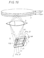
- Reflected-back light L R traveled toward the photosensor section 4 is converged near the diffraction limit.
- the photosensor section 4 is disposed at the position such that at least a part of the photosensor screen thereof falls within the diffraction limit, i.e., a distance from the optical axis a of the light emitted from the light emitting section 1 and which intersects the placement reference plane S of the photosensor screen falls within 1.22 ⁇ /NA where ⁇ is the wavelength of the light emitted from the light emitting section 1 and NA is the numerical aperture of the converging means 3.
- a diameter ⁇ s of the light emitted from the light emitting section 1 on the placement reference plane S of the photosensor screen of the photosensor section 4 is selected to be smaller than a diameter ⁇ d of the diffraction limit and the effective photosensor screen of the photosensor section 1 is located outside the diameter ⁇ s of the emitted light. If the semiconductor laser is used as the light source of the light emitting section 1, then the diameter ⁇ s of the emitted light can be limited to about 1 to 2 ⁇ m.
- the light emitted from the light emitting section 1 is radiated on the optical disc of the radiated section 2 disposed at the confocal position through the converging means 3, i.e., converging optical lens. Accordingly, the light that was radiated on and reflected by the optical disc, i.e., reflected-back light containing recorded information is converged again by the converging means 3 and introduced into the photodiode of the photosensor section 4 disposed near the confocal position. Thus, the reflected-back light is photosensed and detected by the photosensor section 4, i.e., converted into an electrical signal and obtained as a reproduced signal.
- the photosensor screen of the photodiode of the photosensor section 4 is disposed at the position including an area in which a distance from the optical axis a is larger than ⁇ s/2 and falls within at least ⁇ d/2, then the reflected-back light from the radiated section 2, i.e., optical disc can reliably be separated from the emitted light and detected by the photosensor section 4.
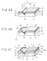
- FIGS. 7A through 7D and FIGS. 8A to 8C An example that the light emitting section 1 and the photosensor section 4 are fabricated on the common substrate 9 as a monolithic structure will be described below with reference to FIGS. 7A through 7D and FIGS. 8A to 8C together with an example of a fabrication method in order to facilitate the understanding of the present invention.
- the substrate 9 formed of a first conductivity type, e.g., n-type GaAs or InP compound semiconductor substrate on which an AlGaAs first cladding layer 22 of first conductivity type, n-type, a GaAs or AlGaAs active layer 23 which is lightly-doped by Al (aluminum) as compared with the first cladding layer 22, an AlGaAs second cladding layer 24 of second conductivity type, e.g., p type and a GaAs capping layer 25 of the same conductivity type are epitaxially grown by MOCVD (metal organic chemical vapor deposition), in that order.
- MOCVD metal organic chemical vapor deposition
- a striped vertical groove 27 with a width of several micrometers is formed near the oblique groove 27a along the striped direction of the oblique groove 27a in the direction perpendicular to the substrate surface with substantially the same depth as that of the substrate 9 by anisotropy etching, such as RIE or the like.
- anisotropy etching such as RIE or the like.
- one resonator end face 28A of the semiconductor laser is formed by the inner side surface of the vertical groove 27 opposite to the oblique groove 27a.
- Another resonator end face 28B also is formed by the surface that is processed by anisotropy etching, such as RIE or the like.
- electrodes 41 and 42 of the semiconductor laser LD and the photodiode PD are respectively deposited on the capping layers 25 of the semiconductor laser LD and the photodiode PD in ohmic contact.
- Another electrode 43 that is common to the semiconductor laser LD and the photodiode PD is deposited on the substrate 9 side in ohmic contact.
- the optical device structure of the present invention since the light path of light traveled to the radiated section 2 and the light path of reflected-back light traveled to the photosensor section 4 are made on the same axis, as far as at least the photosensor section 4 is concerned, the reflected-back light need not be separated from the light path between the light emitting section 1 and the radiated section 2 by some suitable means, such as the beam splitter or the like, the number of optical assembly parts can be reduced and the optical assembly parts can be properly positioned with ease. Thus, accuracy with which respective assembly parts are assembled can be increased, the device structure can be simplified and the assembling and fabrication can be simplified. Concurrently therewith, productivity of optical devices can be increased, reliability of optical device can be improved and the overall structure of optical device can be miniaturized.
Landscapes
- Physics & Mathematics (AREA)
- Optics & Photonics (AREA)
- Condensed Matter Physics & Semiconductors (AREA)
- General Physics & Mathematics (AREA)
- Electromagnetism (AREA)
- Semiconductor Lasers (AREA)
- Optical Head (AREA)
- Led Device Packages (AREA)
- Photo Coupler, Interrupter, Optical-To-Optical Conversion Devices (AREA)
Applications Claiming Priority (6)
| Application Number | Priority Date | Filing Date | Title |
|---|---|---|---|
| JP210691/93 | 1993-08-25 | ||
| JP21069193 | 1993-08-25 | ||
| JP21069193 | 1993-08-25 | ||
| JP5322629A JPH07114746A (ja) | 1993-08-25 | 1993-12-21 | 光学装置 |
| JP32262993 | 1993-12-21 | ||
| JP322629/93 | 1993-12-21 |
Publications (2)
| Publication Number | Publication Date |
|---|---|
| EP0640962A1 true EP0640962A1 (de) | 1995-03-01 |
| EP0640962B1 EP0640962B1 (de) | 1999-07-07 |
Family
ID=26518216
Family Applications (1)
| Application Number | Title | Priority Date | Filing Date |
|---|---|---|---|
| EP94113226A Expired - Lifetime EP0640962B1 (de) | 1993-08-25 | 1994-08-24 | Optische Vorrichtung |
Country Status (6)
| Country | Link |
|---|---|
| US (1) | US5679947A (de) |
| EP (1) | EP0640962B1 (de) |
| JP (1) | JPH07114746A (de) |
| KR (1) | KR100313298B1 (de) |
| DE (1) | DE69419370T2 (de) |
| MY (1) | MY111300A (de) |
Cited By (6)
| Publication number | Priority date | Publication date | Assignee | Title |
|---|---|---|---|---|
| EP0686969A4 (de) * | 1993-12-27 | 1996-05-22 | Sony Corp | Optische vorrichtung |
| EP0731456A3 (de) * | 1995-03-04 | 1996-09-25 | Sony Corp | |
| EP0763821A1 (de) * | 1995-09-13 | 1997-03-19 | Sony Corporation | Optische Vorrichtung |
| US5732060A (en) * | 1995-03-04 | 1998-03-24 | Sony Corporation | Optical pickup and optical recording medium reproducing apparatus having a wire grid unit |
| US5801880A (en) * | 1994-09-21 | 1998-09-01 | Sony Corporation | Confocal microscope with optical recording and reproducing apparatus |
| EP0671734B1 (de) * | 1994-03-08 | 2001-05-16 | Sony Corporation | Optische Vorrichtung |
Families Citing this family (32)
| Publication number | Priority date | Publication date | Assignee | Title |
|---|---|---|---|---|
| KR970700356A (ko) * | 1994-11-10 | 1997-01-08 | 이데이 노부유키 | 광 픽업 장치 및 광학 디스크 드라이브 장치(Optical pickup apparatus and optical disk drive apparatus) |
| AU4307701A (en) | 1999-12-02 | 2001-06-12 | Teraconnect, Inc. | Method and apparatus for reading out and writing to an optical disc |
| JP2001256665A (ja) * | 2000-01-07 | 2001-09-21 | Rohm Co Ltd | 受発光複合素子およびそれを用いた光ピックアップ装置 |
| US6392257B1 (en) | 2000-02-10 | 2002-05-21 | Motorola Inc. | Semiconductor structure, semiconductor device, communicating device, integrated circuit, and process for fabricating the same |
| US6693033B2 (en) * | 2000-02-10 | 2004-02-17 | Motorola, Inc. | Method of removing an amorphous oxide from a monocrystalline surface |
| KR20030011083A (ko) | 2000-05-31 | 2003-02-06 | 모토로라 인코포레이티드 | 반도체 디바이스 및 이를 제조하기 위한 방법 |
| AU2001277001A1 (en) | 2000-07-24 | 2002-02-05 | Motorola, Inc. | Heterojunction tunneling diodes and process for fabricating same |
| US20020096683A1 (en) * | 2001-01-19 | 2002-07-25 | Motorola, Inc. | Structure and method for fabricating GaN devices utilizing the formation of a compliant substrate |
| WO2002082551A1 (en) | 2001-04-02 | 2002-10-17 | Motorola, Inc. | A semiconductor structure exhibiting reduced leakage current |
| US6709989B2 (en) | 2001-06-21 | 2004-03-23 | Motorola, Inc. | Method for fabricating a semiconductor structure including a metal oxide interface with silicon |
| US6992321B2 (en) | 2001-07-13 | 2006-01-31 | Motorola, Inc. | Structure and method for fabricating semiconductor structures and devices utilizing piezoelectric materials |
| US6693298B2 (en) | 2001-07-20 | 2004-02-17 | Motorola, Inc. | Structure and method for fabricating epitaxial semiconductor on insulator (SOI) structures and devices utilizing the formation of a compliant substrate for materials used to form same |
| US7019332B2 (en) * | 2001-07-20 | 2006-03-28 | Freescale Semiconductor, Inc. | Fabrication of a wavelength locker within a semiconductor structure |
| US6855992B2 (en) | 2001-07-24 | 2005-02-15 | Motorola Inc. | Structure and method for fabricating configurable transistor devices utilizing the formation of a compliant substrate for materials used to form the same |
| US20030026310A1 (en) * | 2001-08-06 | 2003-02-06 | Motorola, Inc. | Structure and method for fabrication for a lighting device |
| US20030034491A1 (en) | 2001-08-14 | 2003-02-20 | Motorola, Inc. | Structure and method for fabricating semiconductor structures and devices for detecting an object |
| US6673667B2 (en) * | 2001-08-15 | 2004-01-06 | Motorola, Inc. | Method for manufacturing a substantially integral monolithic apparatus including a plurality of semiconductor materials |
| US20030071327A1 (en) | 2001-10-17 | 2003-04-17 | Motorola, Inc. | Method and apparatus utilizing monocrystalline insulator |
| US6916717B2 (en) | 2002-05-03 | 2005-07-12 | Motorola, Inc. | Method for growing a monocrystalline oxide layer and for fabricating a semiconductor device on a monocrystalline substrate |
| US7169619B2 (en) * | 2002-11-19 | 2007-01-30 | Freescale Semiconductor, Inc. | Method for fabricating semiconductor structures on vicinal substrates using a low temperature, low pressure, alkaline earth metal-rich process |
| US6885065B2 (en) | 2002-11-20 | 2005-04-26 | Freescale Semiconductor, Inc. | Ferromagnetic semiconductor structure and method for forming the same |
| US6806202B2 (en) | 2002-12-03 | 2004-10-19 | Motorola, Inc. | Method of removing silicon oxide from a surface of a substrate |
| US6963090B2 (en) | 2003-01-09 | 2005-11-08 | Freescale Semiconductor, Inc. | Enhancement mode metal-oxide-semiconductor field effect transistor |
| US6965128B2 (en) | 2003-02-03 | 2005-11-15 | Freescale Semiconductor, Inc. | Structure and method for fabricating semiconductor microresonator devices |
| JP4077348B2 (ja) * | 2003-03-17 | 2008-04-16 | 松下電器産業株式会社 | 半導体レーザ装置およびそれを用いた光ピックアップ装置 |
| US7333684B2 (en) * | 2004-03-25 | 2008-02-19 | Integrated Crystal Technology Incorporated | Stack-integrated package of optical transceiver for single core full duplex fiber communications |
| JP2008059645A (ja) * | 2006-08-30 | 2008-03-13 | Hitachi Ltd | 記録用ヘッド |
| JP5085988B2 (ja) * | 2007-06-21 | 2012-11-28 | 株式会社日立製作所 | 光素子集積ヘッドの製造方法 |
| JP5592121B2 (ja) * | 2010-02-17 | 2014-09-17 | セイコーインスツル株式会社 | 近接場光利用ヘッドジンバルアセンブリ及びそれを備えた情報記録再生装置 |
| US11456577B2 (en) * | 2020-07-28 | 2022-09-27 | Raytheon Company | Monolithic quantum cascade laser (QCL)/avalanche photodiode (APD) infrared transceiver |
| WO2022029841A1 (ja) * | 2020-08-03 | 2022-02-10 | 株式会社京都セミコンダクター | 受光素子ユニット |
| CN115430937B (zh) * | 2022-11-08 | 2023-03-24 | 苏州创鑫激光科技有限公司 | 一种激光器及激光加工设备 |
Citations (6)
| Publication number | Priority date | Publication date | Assignee | Title |
|---|---|---|---|---|
| EP0199565A2 (de) * | 1985-04-22 | 1986-10-29 | Sony Corporation | Halbleiterlaservorrichtung für optischen Kopf |
| JPS6258432A (ja) * | 1985-09-06 | 1987-03-14 | Olympus Optical Co Ltd | 集積型光ピツクアツプヘツド |
| EP0244827A2 (de) * | 1986-05-06 | 1987-11-11 | Wai-Hon Lee | Optischer Kopf |
| JPH01303638A (ja) * | 1988-05-31 | 1989-12-07 | Matsushita Electric Ind Co Ltd | 光ピックアップ装置 |
| JPH02278779A (ja) * | 1989-04-19 | 1990-11-15 | Sony Corp | 光集積回路 |
| EP0555097A1 (de) * | 1992-02-05 | 1993-08-11 | Sharp Kabushiki Kaisha | Gerät zur Wiedergabe optischer Information |
Family Cites Families (8)
| Publication number | Priority date | Publication date | Assignee | Title |
|---|---|---|---|---|
| US4918675A (en) * | 1986-12-04 | 1990-04-17 | Pencom International Corporation | Magneto-optical head with separate optical paths for error and data detection |
| JPH01151022A (ja) * | 1987-12-09 | 1989-06-13 | Sharp Corp | 光ピックアップ装置 |
| JPH0770065B2 (ja) * | 1988-04-20 | 1995-07-31 | シャープ株式会社 | 光ピックアップ装置 |
| JPH01311428A (ja) * | 1988-06-09 | 1989-12-15 | Matsushita Electric Ind Co Ltd | 光ヘッド装置及びこれを用いた光情報装置 |
| JPH0758559B2 (ja) * | 1988-09-02 | 1995-06-21 | シャープ株式会社 | 光ピックアップ装置 |
| US5180909A (en) * | 1990-04-27 | 1993-01-19 | Victor Company Of Japan, Ltd. | Optical pickup using diffracted light |
| US5136152A (en) * | 1990-12-19 | 1992-08-04 | Hoetron, Inc. | Hybrid optical pickup with integrated power emission and reading photodetectors |
| JPH05290403A (ja) * | 1992-04-08 | 1993-11-05 | Matsushita Electric Ind Co Ltd | 光ピックアップヘッド装置 |
-
1993
- 1993-12-21 JP JP5322629A patent/JPH07114746A/ja active Pending
-
1994
- 1994-08-23 MY MYPI94002198A patent/MY111300A/en unknown
- 1994-08-23 KR KR1019940020726A patent/KR100313298B1/ko not_active Expired - Fee Related
- 1994-08-24 EP EP94113226A patent/EP0640962B1/de not_active Expired - Lifetime
- 1994-08-24 DE DE69419370T patent/DE69419370T2/de not_active Expired - Fee Related
-
1996
- 1996-03-11 US US08/613,858 patent/US5679947A/en not_active Expired - Fee Related
Patent Citations (6)
| Publication number | Priority date | Publication date | Assignee | Title |
|---|---|---|---|---|
| EP0199565A2 (de) * | 1985-04-22 | 1986-10-29 | Sony Corporation | Halbleiterlaservorrichtung für optischen Kopf |
| JPS6258432A (ja) * | 1985-09-06 | 1987-03-14 | Olympus Optical Co Ltd | 集積型光ピツクアツプヘツド |
| EP0244827A2 (de) * | 1986-05-06 | 1987-11-11 | Wai-Hon Lee | Optischer Kopf |
| JPH01303638A (ja) * | 1988-05-31 | 1989-12-07 | Matsushita Electric Ind Co Ltd | 光ピックアップ装置 |
| JPH02278779A (ja) * | 1989-04-19 | 1990-11-15 | Sony Corp | 光集積回路 |
| EP0555097A1 (de) * | 1992-02-05 | 1993-08-11 | Sharp Kabushiki Kaisha | Gerät zur Wiedergabe optischer Information |
Non-Patent Citations (3)
| Title |
|---|
| PATENT ABSTRACTS OF JAPAN vol. 11, no. 253 (P - 606) 18 August 1987 (1987-08-18) * |
| PATENT ABSTRACTS OF JAPAN vol. 14, no. 98 (P - 1011) 22 February 1990 (1990-02-22) * |
| PATENT ABSTRACTS OF JAPAN vol. 15, no. 46 (E - 1029) 4 February 1991 (1991-02-04) * |
Cited By (8)
| Publication number | Priority date | Publication date | Assignee | Title |
|---|---|---|---|---|
| EP0686969A4 (de) * | 1993-12-27 | 1996-05-22 | Sony Corp | Optische vorrichtung |
| EP0671734B1 (de) * | 1994-03-08 | 2001-05-16 | Sony Corporation | Optische Vorrichtung |
| US5801880A (en) * | 1994-09-21 | 1998-09-01 | Sony Corporation | Confocal microscope with optical recording and reproducing apparatus |
| US6094411A (en) * | 1994-09-21 | 2000-07-25 | Sony Corporation | Confocal microscope with optical recording and reproducing apparatus |
| EP0731456A3 (de) * | 1995-03-04 | 1996-09-25 | Sony Corp | |
| US5732060A (en) * | 1995-03-04 | 1998-03-24 | Sony Corporation | Optical pickup and optical recording medium reproducing apparatus having a wire grid unit |
| EP0763821A1 (de) * | 1995-09-13 | 1997-03-19 | Sony Corporation | Optische Vorrichtung |
| US5793790A (en) * | 1995-09-13 | 1998-08-11 | Sony Corporation | Optical device |
Also Published As
| Publication number | Publication date |
|---|---|
| KR100313298B1 (ko) | 2001-12-28 |
| EP0640962B1 (de) | 1999-07-07 |
| JPH07114746A (ja) | 1995-05-02 |
| US5679947A (en) | 1997-10-21 |
| MY111300A (en) | 1999-10-30 |
| KR950006734A (ko) | 1995-03-21 |
| DE69419370T2 (de) | 2000-01-27 |
| DE69419370D1 (de) | 1999-08-12 |
Similar Documents
| Publication | Publication Date | Title |
|---|---|---|
| EP0640962B1 (de) | Optische Vorrichtung | |
| EP0763821B1 (de) | Optische Vorrichtung | |
| US4672187A (en) | Focusing error detecting device in head assembly for optical disc | |
| US5608233A (en) | Optical device for magneto-optical disc system | |
| US5708645A (en) | Semiconductor laser device to detect a divided reflected light beam | |
| US5920587A (en) | Optical device and method of manufacturing the same | |
| US6661824B2 (en) | Semiconductor laser device and method for fabricating the same | |
| US5883913A (en) | Optical device | |
| JPWO1995018444A1 (ja) | 光学装置 | |
| US5715227A (en) | Optical pickup device | |
| US5757029A (en) | Triangular pyramidal semiconductor structure and optical device using the same | |
| JP3533273B2 (ja) | 光学装置 | |
| JP3735391B2 (ja) | 光学装置 | |
| JPH07193334A (ja) | 半導体レーザを有する光学素子 | |
| JP2888317B2 (ja) | 光ピックアップ装置 | |
| JPH07193273A (ja) | 光学素子の製造方法 | |
| JPH07192301A (ja) | 光学装置 | |
| JPH0823135A (ja) | 光学装置 | |
| Mizuno et al. | A monolithic confocal laser coupler for an optical pick-up | |
| JPH07193274A (ja) | 光学装置 | |
| JPH0765399A (ja) | 受発光装置及び光学ピックアップ | |
| JP2006060242A (ja) | 光学装置及び光学装置の製造方法 | |
| JPH05303763A (ja) | 光ヘッド |
Legal Events
| Date | Code | Title | Description |
|---|---|---|---|
| PUAI | Public reference made under article 153(3) epc to a published international application that has entered the european phase |
Free format text: ORIGINAL CODE: 0009012 |
|
| AK | Designated contracting states |
Kind code of ref document: A1 Designated state(s): DE FR GB |
|
| 17P | Request for examination filed |
Effective date: 19950802 |
|
| 17Q | First examination report despatched |
Effective date: 19980217 |
|
| GRAG | Despatch of communication of intention to grant |
Free format text: ORIGINAL CODE: EPIDOS AGRA |
|
| GRAG | Despatch of communication of intention to grant |
Free format text: ORIGINAL CODE: EPIDOS AGRA |
|
| GRAH | Despatch of communication of intention to grant a patent |
Free format text: ORIGINAL CODE: EPIDOS IGRA |
|
| GRAH | Despatch of communication of intention to grant a patent |
Free format text: ORIGINAL CODE: EPIDOS IGRA |
|
| GRAH | Despatch of communication of intention to grant a patent |
Free format text: ORIGINAL CODE: EPIDOS IGRA |
|
| GRAA | (expected) grant |
Free format text: ORIGINAL CODE: 0009210 |
|
| AK | Designated contracting states |
Kind code of ref document: B1 Designated state(s): DE FR GB |
|
| REF | Corresponds to: |
Ref document number: 69419370 Country of ref document: DE Date of ref document: 19990812 |
|
| ET | Fr: translation filed | ||
| PLBE | No opposition filed within time limit |
Free format text: ORIGINAL CODE: 0009261 |
|
| STAA | Information on the status of an ep patent application or granted ep patent |
Free format text: STATUS: NO OPPOSITION FILED WITHIN TIME LIMIT |
|
| 26N | No opposition filed | ||
| PGFP | Annual fee paid to national office [announced via postgrant information from national office to epo] |
Ref country code: FR Payment date: 20010810 Year of fee payment: 8 |
|
| PGFP | Annual fee paid to national office [announced via postgrant information from national office to epo] |
Ref country code: DE Payment date: 20010820 Year of fee payment: 8 |
|
| PGFP | Annual fee paid to national office [announced via postgrant information from national office to epo] |
Ref country code: GB Payment date: 20010822 Year of fee payment: 8 |
|
| REG | Reference to a national code |
Ref country code: GB Ref legal event code: IF02 |
|
| PG25 | Lapsed in a contracting state [announced via postgrant information from national office to epo] |
Ref country code: GB Free format text: LAPSE BECAUSE OF NON-PAYMENT OF DUE FEES Effective date: 20020824 |
|
| PG25 | Lapsed in a contracting state [announced via postgrant information from national office to epo] |
Ref country code: DE Free format text: LAPSE BECAUSE OF NON-PAYMENT OF DUE FEES Effective date: 20030301 |
|
| GBPC | Gb: european patent ceased through non-payment of renewal fee |
Effective date: 20020824 |
|
| PG25 | Lapsed in a contracting state [announced via postgrant information from national office to epo] |
Ref country code: FR Free format text: LAPSE BECAUSE OF NON-PAYMENT OF DUE FEES Effective date: 20030430 |
|
| REG | Reference to a national code |
Ref country code: FR Ref legal event code: ST |