EP0642132A2 - Amplificateur de lecture pour mémoire - Google Patents
Amplificateur de lecture pour mémoire Download PDFInfo
- Publication number
- EP0642132A2 EP0642132A2 EP94111969A EP94111969A EP0642132A2 EP 0642132 A2 EP0642132 A2 EP 0642132A2 EP 94111969 A EP94111969 A EP 94111969A EP 94111969 A EP94111969 A EP 94111969A EP 0642132 A2 EP0642132 A2 EP 0642132A2
- Authority
- EP
- European Patent Office
- Prior art keywords
- memory cell
- current
- section
- sense amplifier
- memory
- Prior art date
- Legal status (The legal status is an assumption and is not a legal conclusion. Google has not performed a legal analysis and makes no representation as to the accuracy of the status listed.)
- Granted
Links
Images




Classifications
-
- G—PHYSICS
- G11—INFORMATION STORAGE
- G11C—STATIC STORES
- G11C7/00—Arrangements for writing information into, or reading information out from, a digital store
- G11C7/06—Sense amplifiers; Associated circuits, e.g. timing or triggering circuits
- G11C7/067—Single-ended amplifiers
-
- G—PHYSICS
- G11—INFORMATION STORAGE
- G11C—STATIC STORES
- G11C16/00—Erasable programmable read-only memories
- G11C16/02—Erasable programmable read-only memories electrically programmable
- G11C16/06—Auxiliary circuits, e.g. for writing into memory
- G11C16/26—Sensing or reading circuits; Data output circuits
Definitions
- This invention relates to a memory-unit sense amplifier for memory for reading data from EEPROM or the like.
- Fig. 7 is a functional block diagram showing a microcomputer containing an EEPROM as a memory including a sense amplifier.
- numeral 100 indicates a microcomputer;
- numeral 1 indicates a CPU;
- numeral 2 indicates a mask ROM;
- numeral 3 indicates a RAM;
- numeral 4 indicates an EEPROM;
- numeral 5 indicates a sense amplifier of the EEPROM 4;
- numeral 6 indicates a bus;
- a numeral 7 indicates a terminal group comprising a power source terminal VDD, a ground terminal GND, a reset terminal RST, a clock terminal CLK, input/output terminal I/O, etc.
- Fig. 8 is a circuit diagram showing a conventional sense amplifier.
- numerals 8, 9, 10, 11 and 12 indicate P-channel transistors (hereinafter referred to as "Pch”); and numerals 13, 14, 15, 16, 17 and 18 indicate N-channel transistors (hereinafter referred to as “Nch”). These transistors consist of MOSFETs.
- Numeral 19 indicates an inverter.
- Numerals 101 through 106 indicate signals, wirings, terminals, etc. in different parts of the circuit, of which numeral 101 indicates a wiring leading to a EEPROM memory cell;
- numeral 102 indicates a signal line which is set to "L" level when data is being read out; and
- numeral 106 indicates a terminal generating the output of this sense amplifier.
- Symbol VDD indicates a power source voltage.
- Fig. 9 is a diagram showing the input/output characteristics of the conventional sense amplifier.
- the horizontal axis indicates memory cell current IE; and the vertical axis indicates output voltage Vout output from the output terminal 106.
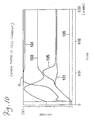
- Figs. 10 and 11 are diagrams showing simulation results obtained with this sense amplifier, of which Fig. 10 shows signal changes in different parts of the circuit shown in Fig. 8 when there is a memory cell current IE, and Fig. 11 shows signal changes in these parts when there is no memory cell current IE.
- the horizontal axis indicates time, and the vertical axis indicates voltage.
- the mask ROM 2 stores user programs for executing various functions necessary in using the microcomputer.
- the CPU 1 upon receiving a reset signal from the terminal RST, the CPU 1 executes a branch routine stored beforehand at a predetermined address in the ROM 2. In the branch routine, branch to a user mode is effected when an user mode execution command is received. In the user mode operation, data input from outside through the I/O terminal is received by the CPU 1 through the bus 6.
- the CPU 1 performs data processing in accordance with a user program stored in the mask ROM 2.
- Data needing temporary storage is stored in the RAM 3, and data needing constant storage, such as processing results, is stored in the EEPROM 4 serving as a data memory.
- the data stored in the EEPROM 4 is read out through the sense amplifier 5. Any data output to the exterior is outwardly transferred through the I/O terminal, etc.
- the gate of the Nch 13 is not charged, so that the Nch 13 does not turn on completely. Therefore, although the potential of the signal 103 becomes somewhat lower than that of the VDD, the Nch 14 and 15 do not turn off. Thus, the voltage of the signal 105 does not increase, and the Pch 11 and 12 turn on, the inverter 19 causing the output signal 106 to be at L level.
- the Nch 13 turns on, and the voltage of the signal 103 is lowered to cause the Nch 14 and 15 to turn off.
- the voltage of the signal 105 is raised by the charging to cause the Nch 16 and 17 to turn on, and the inverter signal 19 causes an H level output signal 106 to be output.
- the Nch 18 is ON except when data is being read out, thereby keeping the signal 105 pulled down to L level.
- the memory cell current detection level of the sense amplifier is determined by the source/gate voltage of the Pch 10 (one of the transistors in the detection result output section) , so that any fluctuations in the power source voltage VDD cause the source/gate voltage of the Pch to fluctuate correspondingly, resulting in great fluctuations being caused in the memory cell current detection level depending on the power source voltage, as shown in Fig. 9.
- the "memory cell current detection level” means the value of the memory cell current IE when the sense amplifier output Vout suddenly changes from the power source voltage level to the ground level. As shown in the drawing, this value increases as the power source voltage VDD increases.
- This invention has been made with a view toward solving the above problem. It is accordingly an object of this invention to provide a memory sense amplifier which restrains the dependence of the memory cell current detection level on the power source voltage so that it can operate in a more stable manner.
- a memory-unit sense amplifier for reading memory cell data
- the memory-unit sense amplifier includes: a detection result output section which outputs a detection result indicative of whether there is any memory cell current or not, detected for the purpose of obtaining the value of memory cell data, to an output amplifying section; and a bias circuit which supplies the gates of transistors in the detection result output section with an output which restrains fluctuations in the source/gate voltage of the transistors due to fluctuations in a power source voltage, whereby the dependence of the memory cell current detection level on the power source voltage is restrained.
- a memory-unit sense amplifier for reading memory cell data, comprising: a detection result output section which outputs a detection result indicative of whether there is any memory cell current or not, detected for the purpose of obtaining the value of memory cell data, to an output amplifying section and which has transistors; a current supplying section which performs wiring-parasitic-capacity charging and which checks whether memory transistors are conducting or not; and a bias circuit which supplies the gates of the transistors of the detection result output section and the gates of the transistors of the current supplying section with an output which restrains fluctuations of the source/gate voltage of these transistors due to fluctuations in power source voltage, wherein the dependence of the memory cell current detection level on the power source voltage is restrained, and, further, overshoot in the current supplying section is prevented.
- a memory-unit sense amplifier wherein the bias circuit further comprises a through-current preventing transistor which separates the bias circuit from the power source except when data is being read out so as to prevent a through-current from flowing through the bias circuit.
- a memory-unit sense amplifier further comprising a level maintaining section which maintains a signal transmission line for transmitting the detection result of the memory cell current detecting section for checking whether there is any memory cell current or not to the detection result output section at a predetermined value except when data is being read out, whereby the signal transmission line is prevented from being put into a floating condition to cause a through-current flow.
- an output of the bias circuit which restrains fluctuations in the source/gate voltage of the transistors of the detection result output section due to fluctuations in the power source voltage, is connected to the gates of the transistors of the detection result output section for outputting the detection result as to whether there is any memory cell current or not, detected for the purpose of obtaining the value of memory cell data, to the output amplifying section, thereby restraining fluctuations in the memory cell current detection level.
- the above-mentioned output of the bias circuit is also connected to the gates of the transistors in the current supplying section which supplies the memory cells with current for the purpose of detecting whether there is any memory cell current or not, performs wiring-parasitic-capacity charging and checks whether memory transistors are conducting or not, whereby the voltage-increase gradient in the section where the parasitic capacity charging is effected is kept constant, thereby preventing overshoot from being generated in the current supplying section.
- the bias circuit further includes a through-current preventing transistor which separates the bias circuit from the power source except when data is being read out so as to prevent a through-current from flowing through the bias circuit, thereby attaining a reduction in power consumption.
- a level maintaining section for maintaining the signal transmission line, which transmits the detection result of the memory cell current detecting section for checking whether there is any memory cell current or not to the detection result output section, at a predetermined value except during operation, whereby the signal transmission line is prevented from being put into the floating state to cause a through-current flow, thereby attaining a reduction in power consumption.
- Fig. 1 is a circuit diagram showing a sense amplifier of a memory unit (EEPROM) according to a first embodiment of the present invention.
- numeral 5a indicates a sense amplifier
- numerals 8, 9, 10, 11, 12 and 23 indicate Pch (P-channel transistors)
- numerals 13, 14, 15, 16, 17 and 18 indicate Nch (N-channel transistors)
- numeral 19 indicates an inverter
- numeral 20 indicates an Nch having a small ⁇ (current amplification factor)
- numerals 21 and 22 indicate diodes formed through diode connection of transistors having a large ⁇ .
- the series circuit composed of the diodes 21 and 22 and the Nch 20 provides a bias circuit which supplies the gate of the Pch 10 with an output which restrains fluctuations of the gate voltage of the Pch 10 due to fluctuations of the power source voltage VDD.
- Numerals 101 through 106 indicate signals, wirings, terminals, etc. in different parts, of which numeral 101 indicates a wiring leading to a memory cell; numeral 102 indicates a signal line which is at L level when data is being read out; and numeral 106 indicates the output terminal and output signal of this sense amplifier.
- Numeral 201 indicates a signal line which is constantly at H level; and numeral 202 indicates the output of the above-described bias circuit.
- Each of the above Pch and Nch transistors consists of a MOSFET.
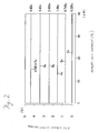
- Fig. 2 is a diagram showing the voltage of the output signal 202 of the bias circuit shown in Fig. 1.
- the horizontal axis indicates memory cell current IE
- the vertical axis indicates values of the voltage of the output signal 202 of the bias circuit with respect to different values of the power source voltage VDD.
- the values of the output signal 202 of the bias circuit shown in Fig. 2 are ones obtained when the Nch 20 has a channel length of 25 ⁇ m and a channel width of 2 ⁇ m, and the diodes 21 and 22 have a channel length of 1.5 ⁇ m and a channel width of 25 u m.
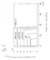
- Fig. 3 is a diagram showing the input/output characteristics of the sense amplifier of Fig. 1.
- the horizontal axis indicates memory cell current IE, and the vertical axis indicates output voltage Vout from the output terminal 106.
- the sense amplifier 5a of Fig. 1 comprises: a data detection circuit which is formed of the components indicated by numerals 8, 9, 10, 13, 14, 15, 18, 20, 21, 22 and 23; and an output amplifying circuit which is formed of the components indicated by numerals 11, 12, 16, 17 and 19 and which amplifies the output of the data detection circuit to convert it into a signal that is at either the power source voltage level or the ground level.
- the series circuit composed of the Pch 9 and the Nch 14 constitutes a current supplying section which supplies the memory cell with a current for the purpose of checking whether there is any memory cell current or not, which effects wiring-parasitic-capacity charging, and which checks whether the memory transistors (not shown) are conducting or not.
- the series circuit composed of the Pch 8 and the Nch 13 constitutes a memory cell current detecting section which checks whether there is any memory cell current or not on the basis of the current supply from the current supplying section (9, 14).
- the series circuit composed of the Pch 10 and the Nch 15 constitutes a detection result output section which outputs detection results in accordance with the detection result as to whether there is any memory cell current or not, obtained by the memory cell current detecting section (8, 13). Further, the wiring 103 provides a signal transmission wiring for transmitting the results obtained by the memory cell current detecting section (8, 13) to the detection result output section (10, 15). Further, the series circuit - composed of the diodes 21 and 22 and the Nch 20, and the Pch 23 constitute a bias circuit for supplying the gates of the transistors of the detection result output section (10, 15) with a voltage in which the influence of fluctuations of the power source voltage has been mitigated.
- the Nch 18 provides an output maintaining section for maintaining, except during operation, the wiring 105, which connects the output of the detection result output section (10, 15) to the output amplifying section (11, 12, 16, 17 and 19) , at a predetermined level (Thus, the output 106 of the output amplifying section is also maintained at a predetermined value).
- the output of the bias circuit is supplied to the gate of the Pch 10, which is a transistor in the detection result output section for outputting the detection results as to the presence of a memory cell current, detected for the purpose of obtaining the memory cell data value, and the fluctuations of the source/gate voltage of the Pch 10 are diminished, thereby further restraining the fluctuations of the memory cell current detection level due to fluctuations in the power source voltage.
- the gate of the Nch 13 is not charged, so that the Nch 13 does not turn on completely. Therefore, the Nch transistors 14 and 15 do not turn off although the voltage of the signal 103 becomes somewhat lower than the VDD. Thus, the voltage of the signal 105 is not increased, and the Pch transistors 11 and 12 turn on, the inverter 19 causing an L-level output signal 106 to be output. Further, the Nch 18 is ON except when data is being read out so as to keep the signal 105 pulled down to L level, and the level of the output signal 106 is fixed.
- the Nch transistors 14 and 15 turn on, and a current starts to flow from the VDD toward the memory cell through the signal portions 104 and 105, thereby effecting parasitic capacity charging on the wiring 101, etc. Further, due to the absence of the memory cell current IE, the memory cell transistors are out of conduction. Thus, when the parasitic capacity charging has been completed, the gate of the Nch 13 is charged, whereby the Nch 13 turns on, and the voltage of the signal 103 is lowered and the Nch 14 and 15 turn off. As a result, the signal 105 is charged to undergo a reduction in voltage, and the Nch 16 and 17 turn on, an H-level output signal 106 being caused to be output by the inverter 19.
- the source/gate voltage of the Pch 10 which is at VDD when data is being read out, fluctuates by the same amount as the VDD.
- bias circuit comprising two diodes, consisting of transistors in diode connection, and one Nch transistor, this should not be construed restrictively. Any type of bias circuit will do as long as it restrains the fluctuations of the source/gate voltage of the Pch 10 with respect to fluctuations in the power source voltage (a bias circuit supplying an output obtained through division of power source voltage).
- Fig. 4 is a circuit diagram showing a memory-unit sense amplifier according to another embodiment of the present invention.
- the sense amplifier shown in Fig. 4 differs from the sense amplifier 5a of Fig. 1 in that the signal 202, which is the output of the bias circuit, is also connected to the gate of the Pch 9, which is a transistor in the current supply section for supplying the memory cell with a current, effecting parasitic capacity charging and checking whether the memory transistors are conducting or not.
- the Nch 14 and 15 turn on, and a current starts to flow from the VDD toward the memory cell through the wiring portions 104 and 105, whereby parasitic capacity charging is effected on the wiring 101 and the bit line (not shown) of the EEPROM memory cell connected thereto, and, due to the presence of the memory cell current, the memory transistors (not shown) conduct.
- the gate of the Nch 13 is not charged, so that the Nch 13 does not turn on completely. Therefore, although the signal 103 becomes somewhat lower in voltage than the VDD, the Nch transistors 14 and 15 do not turn off.
- the signal 105 does not increase in voltage, and the Pch 11 and 12 turn on, an L-level output signal 106 being caused to be output by the inverter 19.
- the Nch 18 turns on to pull the signal 105 down to L level, thereby maintaining the output signal 106 at the fixed level.
- an L-level input signal 102 is input to the gate of the Pch 8
- an H-level input signal 201 is input to the gate of the Nch 20.
- the Pch 8 turns on and the input signal 103 attains H level.
- the Nch transistors 14 and 15 turn on and a current starts to flow from the VDD toward the memory cell through the wiring portions 104 and 105, thereby effecting parasitic capacity charging on the wiring 101, etc. Further, due to the absence of memory cell current, the memory transistors (not shown) are out of conduction. Thus, when the parasitic capacity charging has been completed, the gate of the Nch 13 is charged. Then, the Nch 13 turns on to cause the voltage of the signal 102 to decrease, and the Nch transistors 14 and 15 turn off. As a result, the signal 105 is charged to increase in voltage, and the Nch transistors 16 and 17 turn on, an H-level output signal 106 being caused to be output by the inverter 19. Further, since the signal 202 is also input to the gate of the Pch 9, the voltage increase gradient of the signal 104 is not caused to fluctuate by fluctuations in the VDD.
- the fluctuations in the source/gate voltage of the Pch 9 due to fluctuations of the power source voltage are also restrained, so that the voltage increase gradient of the signal 104 is kept constant, thereby preventing overshoot, which would otherwise cause a malfunction, etc. by excessively increasing the current of the signal 104 (i.e., by causing a needless current flow), as indicated at P in Fig. 10 illustrating the prior art.
- Fig. 5 is a circuit diagram showing a memory-unit sense amplifier according to still another embodiment of the present invention.
- the sense amplifier shown in Fig. 5 differs from that of the second embodiment of Fig. 4 in that a Pch 24 is provided between the diode 21 of the bias circuit, which is composed of the diodes 21 and 22 and the Nch 20, and the power source VDD.
- the Pch 24 is provided as a through-current preventing transistor for separating the bias circuit from the power source VDD except when data is being read out so as to prevent a through-current from flowing through the bias circuit.
- the signal 102 is input to the gate of the Pch 24.
- Fig. 6 is a circuit diagram showing a sense amplifier according to yet another embodiment of the present invention. Since the Nch 18, which pulls down the signal 105 in the above embodiments, turns on except when data is being read out, a through-current flows from the VDD to the GND through the circuit composed of the Pch 10 and the Nch 18. Further, in some cases, the signal 103 is put into a floating state, when a through-current may be allowed to flow. In view of this, in the sense amplifier 5d of this embodiment, the Nch 18 is eliminated and, at the same time, an Nch 25 is provided which serves to keep the signal 103 pulled down to L level except when data is being read out. The signal 102 is input to the gate of the Nch 25.
- the circuit of this embodiment is the same as that of the third embodiment shown in Fig. 5.
- the signal line 103 serves as a signal transmission wiring for transmitting the detection result of the memory cell current detecting section for checking whether there is any memory cell current or not to the detection result output section
- the Nch 25 serves as a level maintaining section for maintaining this signal transmission wiring at a predetermined level except when data is being read out.
- a bias circuit for generating an output in which fluctuations in the power source voltage have been mitigated, and this output of the bias circuit is supplied to the gates of transistors in a detection result output section for outputting a detection result indicative of whether there is any memory cell current or not, detected for the purpose of obtaining the value of memory cell data, to an output amplifying section, thereby restraining fluctuations in the source/gate voltage of the above-mentioned transistors. Due to this arrangement, fluctuations in the memory cell current detection level are restrained, whereby it is possible to provide a sense amplifier which is relatively free from the influence of fluctuations in power source voltage and which operates in a more stable manner.
- the output of the above-mentioned bias circuit is also connected to the gates of transistors in a current supply section which, in order to check whether there is any memory cell current or not, supplies the memory cell with a current, which effects wiring-parasitic-capacity charging and which checks whether memory cell transistors are conducting or not, whereby the voltage increase gradient when the parasitic capacity charging is effected can be kept constant, thereby making it possible to provide a highly reliable sense amplifier in which overshoot is prevented from being generated in this current supply section.
- the above-mentioned bias circuit of the sense amplifier is provided with a through-current preventing transistor which separates the bias circuit from the power source except when data is being read out, so that a through-current is prevented from flowing through the bias circuit except when data is being read out, thereby making it possible to provide a sense amplifier in which a further reduction in power consumption can be attained.
- a level maintaining section which keeps a signal transmission wiring for transmitting the detection result of the memory cell current detecting section, which checks whether there is any memory cell current or not, at a predetermined value except when data is being read out, so that the above-mentioned signal transmission wiring is prevented from being put into a floating state to cause a through-current flow, whereby it is possible to provide a sense amplifier in which a further reduction in power consumption can be attained.
- a memory unit having a sense amplifier for reading data the dependence of the memory cell current detection level of the sense amplifier on the power source voltage is restrained.
- a memory-unit sense amplifier includes a bias circuit (20, 21, 22) for generating an output which mitigates fluctuations in the power source voltage VDD; and a detection result output section (10, 15) which outputs a memory cell current detection result obtained for the purpose of obtaining the value of memory cell data and which has a Pch (P-channel transistor), to the gate of which the output of the bias circuit (20, 21, 22) is connected, whereby fluctuations in the source/gate voltage of the Pch 10 are mitigated so as to restrain the dependence of the memory cell current detection level on the power source voltage.
- a bias circuit (20, 21, 22) for generating an output which mitigates fluctuations in the power source voltage VDD
- a detection result output section (10, 15) which outputs a memory cell current detection result obtained for the purpose of obtaining the value of memory cell data and which has a Pch (P-channel transistor), to the gate of which the output of the bias circuit (20, 21, 22) is connected, whereby fluctuations in the source/gate voltage of the Pch 10 are mitigated so as to restrain the dependence
Landscapes
- Read Only Memory (AREA)
- Static Random-Access Memory (AREA)
- Dram (AREA)
Applications Claiming Priority (2)
| Application Number | Priority Date | Filing Date | Title |
|---|---|---|---|
| JP19113193A JPH0745086A (ja) | 1993-08-02 | 1993-08-02 | メモリ装置 |
| JP191131/93 | 1993-08-02 |
Publications (3)
| Publication Number | Publication Date |
|---|---|
| EP0642132A2 true EP0642132A2 (fr) | 1995-03-08 |
| EP0642132A3 EP0642132A3 (fr) | 1995-04-05 |
| EP0642132B1 EP0642132B1 (fr) | 1999-05-12 |
Family
ID=16269398
Family Applications (1)
| Application Number | Title | Priority Date | Filing Date |
|---|---|---|---|
| EP94111969A Expired - Lifetime EP0642132B1 (fr) | 1993-08-02 | 1994-08-01 | Amplificateur de lecture pour mémoire |
Country Status (4)
| Country | Link |
|---|---|
| US (1) | US5438547A (fr) |
| EP (1) | EP0642132B1 (fr) |
| JP (1) | JPH0745086A (fr) |
| DE (1) | DE69418401T2 (fr) |
Cited By (2)
| Publication number | Priority date | Publication date | Assignee | Title |
|---|---|---|---|---|
| WO1997026656A1 (fr) * | 1996-01-17 | 1997-07-24 | Siemens Aktiengesellschaft | Circuit electronique |
| EP0936621A1 (fr) * | 1998-02-13 | 1999-08-18 | STMicroelectronics S.r.l. | Amplficateur de détection améliorée pour mémoire non volatile avec plage de tensions d'alimentation étendue |
Families Citing this family (1)
| Publication number | Priority date | Publication date | Assignee | Title |
|---|---|---|---|---|
| US8611128B2 (en) * | 2010-10-19 | 2013-12-17 | Freescale Semiconductor, Inc. | ROM memory device |
Family Cites Families (4)
| Publication number | Priority date | Publication date | Assignee | Title |
|---|---|---|---|---|
| JPS59218696A (ja) * | 1983-05-26 | 1984-12-08 | Toshiba Corp | 半導体メモリ |
| US5276369A (en) * | 1989-07-20 | 1994-01-04 | Kabushiki Kaisha Toshiba | Sense amplifier circuit having a bias current control means |
| JPH0752592B2 (ja) * | 1989-08-18 | 1995-06-05 | 株式会社東芝 | 半導体記憶装置 |
| JP3313383B2 (ja) * | 1991-06-27 | 2002-08-12 | 日本電気株式会社 | 読み出し専用記憶装置 |
-
1993
- 1993-08-02 JP JP19113193A patent/JPH0745086A/ja active Pending
-
1994
- 1994-08-01 US US08/283,506 patent/US5438547A/en not_active Expired - Fee Related
- 1994-08-01 EP EP94111969A patent/EP0642132B1/fr not_active Expired - Lifetime
- 1994-08-01 DE DE69418401T patent/DE69418401T2/de not_active Expired - Fee Related
Cited By (3)
| Publication number | Priority date | Publication date | Assignee | Title |
|---|---|---|---|---|
| WO1997026656A1 (fr) * | 1996-01-17 | 1997-07-24 | Siemens Aktiengesellschaft | Circuit electronique |
| EP0936621A1 (fr) * | 1998-02-13 | 1999-08-18 | STMicroelectronics S.r.l. | Amplficateur de détection améliorée pour mémoire non volatile avec plage de tensions d'alimentation étendue |
| US6650147B2 (en) | 1998-02-13 | 2003-11-18 | Stmicroelectronics S.R.L. | Sense amplifier with extended supply voltage range |
Also Published As
| Publication number | Publication date |
|---|---|
| US5438547A (en) | 1995-08-01 |
| EP0642132A3 (fr) | 1995-04-05 |
| EP0642132B1 (fr) | 1999-05-12 |
| DE69418401D1 (de) | 1999-06-17 |
| JPH0745086A (ja) | 1995-02-14 |
| DE69418401T2 (de) | 2000-01-20 |
Similar Documents
| Publication | Publication Date | Title |
|---|---|---|
| EP0136170A2 (fr) | Dispositif de mémoire semi-conductrice | |
| EP1493158B1 (fr) | Amplificateur de detection de courant asymetrique | |
| JPH06236686A (ja) | 半導体装置 | |
| US4912346A (en) | Input/output circuit for IC card | |
| EP0093606A1 (fr) | Circuit pour détecter le niveau de tension | |
| JPS62197988A (ja) | 高利得センスアンプおよびセンスアンプ | |
| US6525967B1 (en) | Fast-sensing amplifier for flash memory | |
| US6239624B1 (en) | Low-power sense amplifier for memory | |
| US5438547A (en) | Memory-unit sense amplifier | |
| EP0459314A2 (fr) | Circuit de verrouillage de bus de données d'un dispositif de mémoire à semi-conducteurs | |
| EP1563507B1 (fr) | Circuit amplificateur cascode pour la production d'une tension de ligne binaire rapide, stable et precise | |
| US4682051A (en) | Voltage level detection circuit | |
| US5898324A (en) | High voltage detector circuit | |
| US4774692A (en) | Sense circuit of a semiconductor memory device | |
| US6885215B1 (en) | Voltage detector circuit with a programmable threshold point | |
| KR950001862A (ko) | 반도체 집적 회로 장치 | |
| EP0508652A1 (fr) | Circuit de mémoire à semi-conducteurs | |
| US6650147B2 (en) | Sense amplifier with extended supply voltage range | |
| US6590821B2 (en) | Memory device | |
| EP0350943B1 (fr) | Circuit intégré semi-conducteur comprenant un circuit tampon de sortie | |
| US7233524B2 (en) | Sense amplifier circuit | |
| KR100343460B1 (ko) | 고전압 검출회로 | |
| KR970010650B1 (ko) | 반도체집적회로의 고전압 검출회로 | |
| US12094543B2 (en) | Memory and sense amplifying device thereof | |
| US6184668B1 (en) | Voltage sensing circuit and method for preventing a low-voltage from being inadvertently sensed as a high-voltage during power-up or power-down |
Legal Events
| Date | Code | Title | Description |
|---|---|---|---|
| PUAI | Public reference made under article 153(3) epc to a published international application that has entered the european phase |
Free format text: ORIGINAL CODE: 0009012 |
|
| PUAL | Search report despatched |
Free format text: ORIGINAL CODE: 0009013 |
|
| AK | Designated contracting states |
Kind code of ref document: A2 Designated state(s): DE FR GB |
|
| AK | Designated contracting states |
Kind code of ref document: A3 Designated state(s): DE FR GB |
|
| 17P | Request for examination filed |
Effective date: 19950502 |
|
| 17Q | First examination report despatched |
Effective date: 19980303 |
|
| GRAG | Despatch of communication of intention to grant |
Free format text: ORIGINAL CODE: EPIDOS AGRA |
|
| GRAG | Despatch of communication of intention to grant |
Free format text: ORIGINAL CODE: EPIDOS AGRA |
|
| GRAH | Despatch of communication of intention to grant a patent |
Free format text: ORIGINAL CODE: EPIDOS IGRA |
|
| GRAH | Despatch of communication of intention to grant a patent |
Free format text: ORIGINAL CODE: EPIDOS IGRA |
|
| GRAA | (expected) grant |
Free format text: ORIGINAL CODE: 0009210 |
|
| AK | Designated contracting states |
Kind code of ref document: B1 Designated state(s): DE FR GB |
|
| REF | Corresponds to: |
Ref document number: 69418401 Country of ref document: DE Date of ref document: 19990617 |
|
| ET | Fr: translation filed | ||
| PLBE | No opposition filed within time limit |
Free format text: ORIGINAL CODE: 0009261 |
|
| STAA | Information on the status of an ep patent application or granted ep patent |
Free format text: STATUS: NO OPPOSITION FILED WITHIN TIME LIMIT |
|
| 26N | No opposition filed | ||
| PGFP | Annual fee paid to national office [announced via postgrant information from national office to epo] |
Ref country code: DE Payment date: 20010723 Year of fee payment: 8 |
|
| PGFP | Annual fee paid to national office [announced via postgrant information from national office to epo] |
Ref country code: GB Payment date: 20010801 Year of fee payment: 8 |
|
| PGFP | Annual fee paid to national office [announced via postgrant information from national office to epo] |
Ref country code: FR Payment date: 20010810 Year of fee payment: 8 |
|
| REG | Reference to a national code |
Ref country code: GB Ref legal event code: IF02 |
|
| PG25 | Lapsed in a contracting state [announced via postgrant information from national office to epo] |
Ref country code: GB Free format text: LAPSE BECAUSE OF NON-PAYMENT OF DUE FEES Effective date: 20020801 |
|
| PG25 | Lapsed in a contracting state [announced via postgrant information from national office to epo] |
Ref country code: DE Free format text: LAPSE BECAUSE OF NON-PAYMENT OF DUE FEES Effective date: 20030301 |
|
| GBPC | Gb: european patent ceased through non-payment of renewal fee |
Effective date: 20020801 |
|
| PG25 | Lapsed in a contracting state [announced via postgrant information from national office to epo] |
Ref country code: FR Free format text: LAPSE BECAUSE OF NON-PAYMENT OF DUE FEES Effective date: 20030430 |
|
| REG | Reference to a national code |
Ref country code: FR Ref legal event code: ST |