EP0642238B1 - Verfahren und Vorrichtung zur Korrektur der Rahmenphase in einem System mit Teilnehmeranschlussleitung mit Träger - Google Patents
Verfahren und Vorrichtung zur Korrektur der Rahmenphase in einem System mit Teilnehmeranschlussleitung mit Träger Download PDFInfo
- Publication number
- EP0642238B1 EP0642238B1 EP94101411A EP94101411A EP0642238B1 EP 0642238 B1 EP0642238 B1 EP 0642238B1 EP 94101411 A EP94101411 A EP 94101411A EP 94101411 A EP94101411 A EP 94101411A EP 0642238 B1 EP0642238 B1 EP 0642238B1
- Authority
- EP
- European Patent Office
- Prior art keywords
- phase
- multiframe
- frames
- frame
- counter
- Prior art date
- Legal status (The legal status is an assumption and is not a legal conclusion. Google has not performed a legal analysis and makes no representation as to the accuracy of the status listed.)
- Expired - Lifetime
Links
Images


Classifications
-
- H—ELECTRICITY
- H04—ELECTRIC COMMUNICATION TECHNIQUE
- H04Q—SELECTING
- H04Q11/00—Selecting arrangements for multiplex systems
- H04Q11/04—Selecting arrangements for multiplex systems for time-division multiplexing
-
- H—ELECTRICITY
- H04—ELECTRIC COMMUNICATION TECHNIQUE
- H04J—MULTIPLEX COMMUNICATION
- H04J3/00—Time-division multiplex systems
- H04J3/02—Details
- H04J3/06—Synchronising arrangements
- H04J3/0635—Clock or time synchronisation in a network
- H04J3/0676—Mutual
-
- H—ELECTRICITY
- H04—ELECTRIC COMMUNICATION TECHNIQUE
- H04J—MULTIPLEX COMMUNICATION
- H04J3/00—Time-division multiplex systems
- H04J3/02—Details
- H04J3/06—Synchronising arrangements
- H04J3/0635—Clock or time synchronisation in a network
- H04J3/0638—Clock or time synchronisation among nodes; Internode synchronisation
- H04J3/0647—Synchronisation among TDM nodes
Definitions
- the present invention relates to a method and apparatus for correcting the phase of transmitted data frames, and more particularly to a method and apparatus for correcting the phase of frames/multiframes transmitted over incoming lines in subscriber loop carrier systems.
- Subscriber loop carrier systems have been employed to accommodate subscribers, at geographically remote locations from switching offices, economically and with high transmission quality, and also to alleviate the problem of the ever increasing number of telephone cables in urban areas.
- a plurality of subscriber lines are multiplexed as PCM data with a frame/multiframe structure at a remote terminal (RT), and the thus multiplexed PCM data are then transmitted over a fiber optic or other transmission medium to a central office terminal (COT), where the data are demultiplexed into a plurality of subscriber lines for connection to switching equipment.
- RT remote terminal
- COT central office terminal
- a multiplexer for remultiplexing a plurality of multiplexed data is provided with a time slot interchanger (TSI) for interchanging time slots to accomplish dynamic rearrangement on a user-by-user basis.
- TSI time slot interchanger
- phase correction is done by storing the data in memory at the receiving end. This requires the provision of a memory for storing the data, and furthermore, transmission delays are caused because of temporarily storing the data.
- the phase correction is only necessary for the frame, but no phase correction is needed for the multiframe. In this case, a memory that can store one frame of data will suffice for the purpose, and the transmission delay can be kept within one frame period.
- the phase correction must be done not only for the frame but for the multiframe that typically consists of 12 frames. In such a case, the memory capacity required will be much larger, and significant transmission delays will result.
- TCM time compression multiplexing
- the oscillator frequency at a receiving end is controlled on the basis of advance (A), retard (R) and out-of-limits (OL) signals from the transmitting end and A, R and OL signals made at the receiving end.
- GB-A-1 577 331 in which the clock frequency of a switching center receiving end is controlled based on incoming A-R-Z at a ("advance”, “retard” and “do-nothing” signals) transmitted from a switching center at a transmitting end and the local A-R-Z.
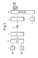
- Fig. 1 is a diagram showing the basic configuration of a subscriber loop carrier system in which an embodiment of the present invention is incorporated; the overall configuration of the system is shown here in a simplified form.
- the numeral 1 designates a subscriber interface (CH), provided for each subscriber, and via which an analog signal from the subscriber (telephone) side is converted to a PCM signal for transmission over each individual channel and vice versa.
- a low-order channel interface (CH inf) 2 is provided via which PCM signals from the individual channels are multiplexed into or demultiplexed from a multiframe signal.
- Line terminations (LT) 3 and 4 each perform conversion between a multiplexed signal and a signal transmitted or for transmission over an optical or metallic transmission path 5.
- a multiplexer 6 converts the multiplexed signals into a higher-level multiplexed signal for connection to a switching network and vice versa.
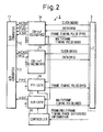
- Fig. 2 is a diagram showing the configuration of a low-order channel interface according to one embodiment of the invention.
- the numeral 11 is a codec which consists of a digital-to-analog (D/A) converter 12 for converting PCM signals into analog signals, and an analog-to-digital (A/D) converter 13 for converting analog signals into PCM signals.
- D/A digital-to-analog
- A/D analog-to-digital
- a channel interface converter (CH-inf) 14 for outgoing lines separates multiframe-structured data (VFR) transferred from the LT 3 into PCM signals for individual channels by using a clock (MCKR), frame timing pulse (FPR), and multiframe timing pulse (ABR), and transfers data (VFR') to the respective D/A converter units 12 together with a clock (MCKR'), frame timing pulse (FPR'), and multiframe timing pulse (ABR').
- MCKR clock
- FPR frame timing pulse
- ABR multiframe timing pulse
- a channel interface converter (CH-inf) 15 for incoming lines supplies a clock (MCKS') to the A/D converter 13 for each channel in response to a clock (MCKS) fed from the LT 3, and multiplexes data (VFS'), i.e. PCM signals supplied from the A/D converter 13 in synchronism with the clock (MCKS'), into frame/multiframe-structured data (VFS) which is transferred to the LT 3.
- CH-inf multiplexes data
- MCKS' multiplexes data supplied from the A/D converter 13 in synchronism with the clock (MCKS') into frame/multiframe-structured data (VFS) which is transferred to the LT 3.
- a frame timing generator (FP-GEN) 16 performs phase correction on the frame timing pulse (FPR) fed from the LT 3 by using frame timing phase difference information supplied from a controller 18, and produces outputs, one being supplied to the LT 3 as a frame timing pulse (FPS) and the other supplied to the A/D converter 13 as a frame timing pulse (FPS') for each channel.
- FPR frame timing pulse
- FPS frame timing pulse
- FPS' frame timing pulse
- a multiframe timing generator (AB-GEN) 17 performs phase correction on the multiframe timing pulse (ABR) fed from the LT 3 by using multiframe timing phase difference information supplied from the controller 18, and produces outputs, one being supplied to the LT 3 as a multiframe timing pulse (ABS) and the other supplied to the A/D converter 13 as a multiframe timing pulse (ABS') for each channel.
- ABR multiframe timing pulse
- ABS multiframe timing pulse
- the controller 18 supplies the frame timing phase difference information to the FP-GEN 16 and the multiframe phase difference information to the AB-GEN 17 in accordance with frame/multiframe timing phase difference information supplied from the multiplexer 6 (Fig. 3).
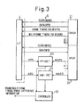
- Fig. 3 is a diagram showing the configuration of a multiplexer as used in one embodiment of the invention, wherein the same parts as those shown in Fig. 1 are designated by the same numerals.
- the multiplexer 6 consists of a demultiplexing unit (DMUX) 21 for demultiplexing a higher-level multiplexed signal, and a multiplexing unit (MUX) 22 for multiplexing lower-level multiplexed signals into a higher-level multiplexed signal.
- the DMUX 21 demultiplexes the higher-level multiplexed signal and distributes each of the demultiplexed multiframe data (VFR) to the LT 4 together with a clock (MCKR), frame timing pulse (FPR), and multiframe timing pulse (ABR).
- MCKR clock
- FPR frame timing pulse
- ABR multiframe timing pulse
- the MUX 22 sends a clock (MCKS) to the LT 4 and multiplexes data (VFS) from the LT 4 into a higher-level multiplexed signal for transmission to higher-order equipment.
- MCKS clock
- VFS multiplexes data
- a frame phase difference detector (FP-DET) 23 compares a frame timing pulse (MFPS) fed from the MUX 22 with a frame timing pulse (FPS) fed from the LT 4, and produces frame timing phase difference information.
- a multiframe phase difference detector (AB-DET) 24 compares a multiframe timing pulse (MABS) fed from the MUX 22 with a multiframe timing pulse (ABS) fed from the LT 4, and produces multiframe timing phase difference information.
- a controller 25 transmits the frame timing phase difference information from the FP-DET 23 and the multiframe timing phase difference information from the AB-DET 24 to the controller 18 (Fig. 2) in the low-order channel interface 2.
- the frame phase difference and the multiframe phase difference occurring between the MUX 22 and the LT 4 are detected in the multiplexer 6, and the detected information is transmitted to the low-order channel interface 2, where, based on this information, the phase differences of the frame timing and multiframe timing pulses between the A/D converter 13 and the LT 3 are corrected, compensating for differences in delay time between LT 3 and LT 4 and thus reducing the phase differences of the frame and multiframe signals, respectively, to zero.
- Fig. 4 shows the timing for the various signals in association with the frame structure.
- one frame consists of 24 time slots (TS), but this is only illustrative and not restrictive.
- VFS/R indicates frame-structured data for incoming and outgoing lines.
- TS1 to TS24 are time slots; each TS consists of 8-bit data, b1 to b8, and a 1-bit framing bit (F) is added at the beginning of the frame, so that each frame consists of a total of 193 bits (in 125 ⁇ s).
- FPS/R is a frame timing pulse for incoming and outgoing lines
- MFPS is a frame timing pulse output from the multiplexer 6
- MCKS/R is a clock signal for incoming and outgoing lines.
- Fig. 5 shows the timing of the various signals in association with the multiframe structure.
- one multiframe consists of 12 frames, but this is only illustrative and not restrictive.
- VFS/R indicates multiframe-structured data for incoming and outgoing lines.
- F1 to F12 are frames each corresponding to the 193-bit frame illustrated in Fig. 4.
- ABS is a multiframe timing pulse for incoming lines
- MABS is a multiframe timing pulse output from the multiplexer 6
- ABR is a multiframe timing pulse for outgoing lines
- FPS/R is a frame timing pulse for incoming and outgoing lines
- MCKS/R is a clock signal for incoming and outgoing lines.
- Fig. 6 is a circuit block diagram showing a configurational example of the frame phase difference detector (or multiframe phase difference detector). These detectors can be easily implemented using relatively simple logic circuits.
- the signals associated with the multiframe phase difference detector 24 are shown in square brackets along with the corresponding signals associated with the frame phase difference detector 23.
- the numeral 31 indicates a counter which counts the number of clock pulses (MCKS) or frame timing pulses (MFPS), starting from the pulse position of the frame timing pulse (MFPS) or multiframe timing pulse (MABS) applied at a start signal input (STR) from the MUX 22 and ending at the pulse position of the frame timing pulse (FPS) or multiframe timing pulse (ABS) applied at a stop signal input (STP) from the LT 4.
- the resulting counter value is latched into a counter value holding latch 32 before transfer to the controller 25.
- Delay circuits 33 and 34 are provided which delay the frame timing pulse (FPS) or multiframe timing pulse (MFPS) in accordance with the clock (MCKS) or frame timing pulse (MFPS), and which produce a latch timing signal for the counter value holding latch 32 and a reset signal for the counter 31, respectively.
- FPS frame timing pulse
- MFPS multiframe timing pulse
- MCKS clock
- MFPS frame timing pulse
- the counter 31 is started by the application of MFPS or MABS, and stopped by the application of FPS or ABS, upon which the counter value is read out. It will be appreciated, however, that the counter value may also be read out by starting the counting upon FPS or ABS and stopping it upon MFPS or MABS.
- Fig. 7 is a circuit block diagram showing a configurational example of the frame timing generator (multiframe timing generator). These generators also can be easily implemented using relatively simple logic circuits. In the figure, the signals associated with the multiframe timing generator 17 are shown in square brackets along with the corresponding signals associated with the frame timing generator 16.
- the numeral 41 indicates a data buffer where the phase correction data from the controller 18 is stored.
- a counter 42 is reset by the frame timing pulse (FPR) or multiframe timing pulse (ABR) applied from the LT 3, and counts the number of clock pulses (MCKR) or frame timing pulses (FPR) by a period equal to the phase correction data written in the data buffer 41.
- a signal is output from a carry signal output (CO) whereby an FPS [ABS] timing generator 44 is driven to generate frame timing pulses (FPS, FPS') or multiframe timing pulses (ABS, ABS').
- a delay circuit 43 delays FPR or ABR and supplies the resulting output to the data buffer 41 as a loading signal by which the phase correction data is written into the data buffer 41 immediately after the resetting of the counter 42.
- the FPS [ABS] timing generator 44 At the completion of the counting by the counter 42, the FPS [ABS] timing generator 44 generates the frame timing pulses (FPS, FPS') or the multiframe timing pulses (ABS, ABS').
- Figs. 8 and 9 are flowcharts illustrating the operations of the controllers: Fig. 8 for the controller 25 and Fig. 9 for the controller 18.
- the controller 25 reads the frame phase difference data and multiframe phase difference data from the frame phase difference detector 23 and multiframe phase difference detector 24, respectively, and transmits the phase difference data to the controller 18 if the frame phase difference or multiframe phase difference is not zero. Then, after waiting for a prescribed time, the operation returns to the beginning of the control process. The prescribed waiting time is inserted to perform the control in an intermittent manner.
- the controller 18 when the phase difference data is received from the controller 25, the controller 18 writes the frame phase difference data into the frame timing generator 16 and the multiframe phase difference data into the multiframe timing generator 17.
- the processing in the controllers 18 and 25 is implemented in software, but since the processing is relatively simple, it can also be easily implemented in hardware using logic circuits.
- Communication between the controllers 18 and 25 is accomplished, for example, by using overhead bits appended to the data transmitted between the LT 3 and LT 4.
Landscapes
- Engineering & Computer Science (AREA)
- Computer Networks & Wireless Communication (AREA)
- Signal Processing (AREA)
- Time-Division Multiplex Systems (AREA)
- Synchronisation In Digital Transmission Systems (AREA)
Claims (10)
- Rahmenphasenkorrekturverfahren zur Korrektur der Phase von Datenrahmen an einem empfangenden Ende für die zu dem empfangenden Ende von einem sendenden Ende gesendeten Daten, die Schritte umfassend:a) Erfassen einer Phasendifferenz (23) zwischen der Phase (FPS) empfangener Rahmen (FPS) und einer Referenzphase (MFPS) am empfangenden Ende (6); undb) Senden der erfassten Rahmenphasendifferenz zu der Sendeseite (2);
gekennzeichnet durchc) Steuern (16, 18) der Phase von am sendenden Ende (2) gebildeten Rahmen in Übereinstimmung mit der Rahmenphasendifferenz, die von dem empfangenden Ende (6) zugeführt worden ist, wodurch Phasenkorrektur vorgenommen wird, ohne sich auf Speicherspeichern zu verlassen. - Verfahren nach Anspruch 1, dadurch gekennzeichnet, dass eine vorgeschriebene Zahl aufeinanderfolgender Rahmen in einer Gruppe zusammengefasst sind zum Bilden eines Mehrfachrahmens (F1-F12) und ferner die Schritte umfassend:d) Erfassen einer Phasendifferenz (24) zwischen der Phase empfangener Mehrfachrahmen (ABS) und einer Referenzphase (MABS) am empfangenden Ende;e) Senden der erfassten Mehrfachrahmenphasendifferenz zu dem sendenden Ende (2); undf) Steuern (17, 18) der Phase von am sendenden Ende (2) gebildeten Mehrfachrahmen auf der Basis der Mehrfachrahmenphasendifferenz.
- Verfahren nach Anspruch 2, dadurch gekennzeichnet, dass die Rahmenphase (FPS) und die Mehrfachrahmenphase (ABS) jeweils die Phasen der Rahmen und Mehrfachrahmen aus kommenden Leitungen in einem Teilnehmerschleifenträgersystem repräsentieren.
- Verfahren nach Anspruch 3, dadurch gekennzeichnet, dass der Schritt a) die Unterschritte einschließt:wobei der Zählerwert eine Angabe bereitstellt bezüglich der Phasendifferenz, undStarten eines ersten Zählers (31) durch eines von die Referenzphase oder die Phase der empfangenen Rahmen repräsentieren Impulsen, undLesen eines Zählerwertes von dem ersten Zähler (31) ansprechend auf den Empfang des anderen von den die Referenzphase oder die Phase von empfangenen Rahmen repräsentierenden Impulsen,
dass der Schritt c) die Unterschritte einschließt:Laden des Zählerwertes in einen zweiten Zähler (42) durch den die Referenzphase repräsentierenden Impuls, undBestimmen der Phase der in Übereinstimmung mit einer Zählendesignalausgangsgröße von dem zweiten Zähler (42) gebildeten Rahmen. - Verfahren nach Anspruch 3, dadurch gekennzeichnet, dass der Schritt d) den Unterschritt einschließt:dass der Schritt f) die Unterschritte einschließt:Starten eines Zählers (31) durch eines von die Referenzphase (MABS) oder die Phase (ABS) der empfangen Mehrfachrahmen repräsentierenden Impulsen, undLesen eines Zählerwertes von dem Zähler (31) durch den anderen (ABS, MABS) von den die Referenzphase (MABS) oder die Phase (ABS) der empfangenen Mehrfachrahmen repräsentierenden Impulse, wobei der Zählerwert eine Angabe der Phasendifferenz bereitstellt, undLaden des Zählerwertes in einen ferneren Zähler (42) durch den die Referenzphase repräsentierenden Impuls, undBestimmen der Phase der Mehrfachrahmen (F1-F12), die in Übereinstimmung mit einer von dem ferneren Zähler (42) ausgegebenen Zählendesignals zu bilden ist.
- Rahmenphasenkorrektureinrichtung zum Korrigieren der Phasen von Datenrahmen an einem empfangenden Ende für die zu dem empfangenden Ende von einem sendenden Ende gesendeten Daten, umfassend:a) eine Vorrichtung (23) zum Erfassen einer Phasendifferenz zwischen der Phase (FPS) empfangener Rahmen und eine Referenzphase (MFPS) am empfangenden Ende; undb) eine Vorrichtung zum Senden der von der Rahmenphasendifferenzerfassungsvorrichtung (23, 24) erfassten Rahmenphasendifferenz zu dem sendenden Ende (28);
gekennzeichnet durchc) eine Vorrichtung (18) zum Steuern der Phase von am sendenden Ende (2) gebildeten Rahmen in Übereinstimmung mit der von dem empfangenden Ende (6) zugeführten Rahmenphasendifferenz, wodurch Phasenkorrektur ausgeführt wird, ohne sich auf Speicherspeichern zu verlassen. - Einrichtung nach Anspruch 6, dadurch gekennzeichnet, dass eine vorgeschriebene Zahl von aufeinanderfolgenden Rahmen (F1-F2) in einer Gruppe zusammengefasst sind zum Bilden eines Mehrfachrahmens, ferner umfassend:eine Vorrichtung (23) zum Erfassen einer Phasendifferenz zwischen der Phase von empfangenen Mehrfachrahmen (ABS) und einer Referenzphase (MABS) am empfangenden Ende;eine Vorrichtung (5) zum Senden der von der Mehrfachrahmenphasenerfassungsvorrichtung (24) erfassten Mehrfachrahmenphasendifferenz zu dem sendenden Ende (2, 3); undeine Vorrichtung (18) zum Steuern der Phase von am sendenden Ende (2, 3) gebildeten Mehrfachrahmen, basierend auf der Mehrfachrahmenphasendifferenz.
- Einrichtung nach Anspruch 7, dadurch gekennzeichnet, dass die Rahmenphase und die Mehrfachrahmenphase jeweils die Phasen der Rahmen (T1-T24) und Mehrfachrahmen (F1-F19) auf kommenden Leitungen in einem Teilnehmerschleifenträgersystem repräsentieren.
- Einrichtung nach Anspruch 8, dadurch gekennzeichnet, dass die Rahmenphasendifferenzerfassungsvorrichtung (23, 24) einen ersten Zähler (31) einschließt, der gestartet wird durch eines von die Referenzphase (MFPS, ABS) oder die Phase der empfangenen Rahmen (FPS, ABS) repräsentierenden Impulse und von welchem ein Zählerwert ausgelesen wird durch den anderen von den die Referenzphase oder die Phase der empfangenen Rahmen repräsentierenden Impulse, und
dass die Rahmenphasensteuervorrichtung (18) einen zweiten Zähler (42) einschließt, in welchen der Zählwert durch den die Referenzphase (MFPS, ABS) repräsentierenden Impuls geladen wird, und welcher eingerichtet ist, um ein Zählendesignal auszugeben, und eine Rahmenzeitabstimmungsgeneriervorrichtung (44), welche eingerichtet ist zum Ausgeben eines Impulses zum Bestimmen der Phase von zu bildenden Rahmen in Übereinstimmung mit dem Zählendesignal. - Einrichtung nach Anspruch 9, dadurch gekennzeichnet, dass die Mehrfachrahmenphasendifferenzerfassungsvorrichtung (24) einen dritten Zähler (31) einschließt, welcher gestartet wird durch eines von den die Referenzphase (MABS) oder die Phase der empfangenen Mehrfachrahmen (ABS) repräsentierenden Impulse, und von welchem ein Zählwert ausgelesen wird durch den anderen von den die Referenzphase oder die Phase der empfangenen Mehrfachrahmen repräsentierenden Impulse, und
dass die Mehrfachrahmenphasensteuervorrichtung einen vierten Zähler (42) einschließt (18), in welchen der Zählwert durch den die Referenzphase repräsentierenden Impuls geladen wird und welcher eingerichtet ist zum Ausgeben eines Zählendesignals, und eine Mehrfachrahmenzeitabstimmungsgeneriervorrichtung (44), welche eingerichtet ist zum Ausgeben eines Impulses zum Bestimmen der Phase des zu bildenden Mehrfachrahmens in Übereinstimmung mit dem Zählendesignal.
Applications Claiming Priority (3)
| Application Number | Priority Date | Filing Date | Title |
|---|---|---|---|
| JP22322493 | 1993-09-08 | ||
| JP223224/93 | 1993-09-08 | ||
| JP5223224A JPH0779209A (ja) | 1993-09-08 | 1993-09-08 | フレーム/マルチフレーム位相補正方式 |
Publications (3)
| Publication Number | Publication Date |
|---|---|
| EP0642238A2 EP0642238A2 (de) | 1995-03-08 |
| EP0642238A3 EP0642238A3 (de) | 1995-09-20 |
| EP0642238B1 true EP0642238B1 (de) | 2004-05-12 |
Family
ID=16794743
Family Applications (1)
| Application Number | Title | Priority Date | Filing Date |
|---|---|---|---|
| EP94101411A Expired - Lifetime EP0642238B1 (de) | 1993-09-08 | 1994-01-31 | Verfahren und Vorrichtung zur Korrektur der Rahmenphase in einem System mit Teilnehmeranschlussleitung mit Träger |
Country Status (4)
| Country | Link |
|---|---|
| US (1) | US5528609A (de) |
| EP (1) | EP0642238B1 (de) |
| JP (1) | JPH0779209A (de) |
| DE (1) | DE69433770T2 (de) |
Families Citing this family (10)
| Publication number | Priority date | Publication date | Assignee | Title |
|---|---|---|---|---|
| JPH08228183A (ja) * | 1995-02-20 | 1996-09-03 | Fujitsu Ltd | 信号処理装置及び信号処理方法 |
| US5828670A (en) * | 1995-06-06 | 1998-10-27 | Symmetricom, Inc. | Distribution of synchronization in a synchronous optical environment |
| DE19523489A1 (de) * | 1995-06-28 | 1997-01-02 | Sel Alcatel Ag | Verfahren und Schaltungsanordnung zur Synchronisation von Impulsrahmen in multizellularen Telekommunikationsanlagen |
| GB2324214A (en) | 1997-04-08 | 1998-10-14 | Power X Limited | Synchronising arrangements |
| IL123045A0 (en) | 1998-01-25 | 1998-09-24 | Eci Telecom Ltd | Apparatus and method for digital telephony |
| US6287306B1 (en) | 1998-06-22 | 2001-09-11 | Daig Corporation | Even temperature linear lesion ablation catheter |
| KR100497351B1 (ko) * | 2001-02-08 | 2005-06-23 | 삼성전자주식회사 | 시분할 다중화에 따른 위상 불일치 보상 장치 및 방법 |
| ATE279056T1 (de) * | 2002-05-02 | 2004-10-15 | Cit Alcatel | Verfahren zur phasenkontrolle eines datensignales,schaltungsanordnung für gegenläufigem takt und interface-vorrichtung |
| JP4448076B2 (ja) * | 2005-09-16 | 2010-04-07 | 富士通株式会社 | データ送受信回路のタイミング調整回路、lsi及びデータ送受信システム |
| US20070183462A1 (en) | 2006-02-04 | 2007-08-09 | Daugherty Charles H | Method and apparatus for aligning source data streams in a communications network |
Family Cites Families (9)
| Publication number | Priority date | Publication date | Assignee | Title |
|---|---|---|---|---|
| US3562432A (en) * | 1966-11-16 | 1971-02-09 | Communications Satellite Corp | Synchronizer for time division multiple access satellite communication system |
| GB1508986A (en) * | 1974-05-29 | 1978-04-26 | Post Office | Digital network synchronising system |
| GB1577331A (en) * | 1976-06-19 | 1980-10-22 | Plessey Co Ltd | Synchronisation arrangements for digital switching centres |
| JPS57168545A (en) * | 1981-04-09 | 1982-10-16 | Fujitsu Ltd | Controlling system for frame ttransfer phase |
| JPS6124338A (ja) * | 1984-07-12 | 1986-02-03 | Nec Corp | 多方向多重通信方式 |
| US5091899A (en) * | 1988-02-04 | 1992-02-25 | Matsushita Electric Industrial Co., Ltd. | Time code recording or reproducing apparatus and time code converter |
| EP0439630B1 (de) * | 1989-08-25 | 1996-02-07 | Nippon Telegraph And Telephone Corporation | Regelungsverfahren eines funkkanalschalters |
| JP2512586B2 (ja) * | 1990-03-08 | 1996-07-03 | 富士通株式会社 | フレ―ム同期依存型ビット同期抽出回路 |
| US5140616A (en) * | 1990-11-19 | 1992-08-18 | Ag Communication Systems Corporation | Network independent clocking circuit which allows a synchronous master to be connected to a circuit switched data adapter |
-
1993
- 1993-09-08 JP JP5223224A patent/JPH0779209A/ja not_active Withdrawn
-
1994
- 1994-01-31 US US08/189,408 patent/US5528609A/en not_active Expired - Lifetime
- 1994-01-31 DE DE69433770T patent/DE69433770T2/de not_active Expired - Lifetime
- 1994-01-31 EP EP94101411A patent/EP0642238B1/de not_active Expired - Lifetime
Also Published As
| Publication number | Publication date |
|---|---|
| EP0642238A3 (de) | 1995-09-20 |
| EP0642238A2 (de) | 1995-03-08 |
| US5528609A (en) | 1996-06-18 |
| DE69433770D1 (de) | 2004-06-17 |
| DE69433770T2 (de) | 2005-04-28 |
| JPH0779209A (ja) | 1995-03-20 |
Similar Documents
| Publication | Publication Date | Title |
|---|---|---|
| US5461622A (en) | Method and apparatus for using SONET overheat to align multiple inverse multiplexed data streams | |
| EP0788695B1 (de) | Verfahren zum zerlegen und zusammensetzen von rahmenstrukturen mit zeigern | |
| US6842787B2 (en) | Method and device for converting virtually concatenated data streams into contiguously concatenated data streams | |
| US4143246A (en) | Time division line interface circuit | |
| JPH07170284A (ja) | テレコミュニケーションネットワーク、そのメインステーション及びサブステーション | |
| EP0642238B1 (de) | Verfahren und Vorrichtung zur Korrektur der Rahmenphase in einem System mit Teilnehmeranschlussleitung mit Träger | |
| EP0788694B1 (de) | Verfahren und einrichtung zur elastischen pufferung in einem synchronen digitalen fernmeldesystem | |
| US4595907A (en) | PCM data translating apparatus | |
| US4977558A (en) | Demultiplexing device of synchronous multiplexing system | |
| JP3429309B2 (ja) | 同期デジタル遠隔通信システムにおけるエラスティックバッファメモリの充填率を監視する方法及び装置 | |
| NZ244596A (en) | Synchroniser for asynchronous transfer mode digital network terminal equipment | |
| US4302839A (en) | Multiplex unit with means for responding to signal loss in one or more channels | |
| EP0699363B1 (de) | Verfahren und vorrichtung zum bestimmen einer stopfentscheidung in einem knoten eines synchronen digitalen nachrichtenübertragungssystems (sdh) | |
| JP3246423B2 (ja) | 網同期装置 | |
| GB2285725A (en) | Data burst transfer | |
| US5418788A (en) | Data link terminator | |
| JP3189057B2 (ja) | キャリアリレー信号伝送方法および装置 | |
| EP0136749A1 (de) | Fernsprechvermittlungsstelle welche periphere Steuerzonen umfasst | |
| JP2001119362A (ja) | コントロールタイムスロット中継回路 | |
| HK1011805B (en) | Method and equipment for monitoring the fill rate of an elastic buffer memory in a synchronous digital telecommunication system | |
| KR980007725A (ko) | 엠펙2 동영상 정보의 ds-3급 다중장치 및 다중방법 | |
| JPH10336131A (ja) | バルク伝送装置及びバルク伝送方法 | |
| HK1002378B (en) | Method and equipment for elastic buffering in a synchronous digital telecommunication system | |
| JPH0477137A (ja) | 秘話伝送方式 | |
| JPH04345228A (ja) | 情報伝送方式 |
Legal Events
| Date | Code | Title | Description |
|---|---|---|---|
| PUAI | Public reference made under article 153(3) epc to a published international application that has entered the european phase |
Free format text: ORIGINAL CODE: 0009012 |
|
| AK | Designated contracting states |
Kind code of ref document: A2 Designated state(s): DE FR GB |
|
| PUAL | Search report despatched |
Free format text: ORIGINAL CODE: 0009013 |
|
| AK | Designated contracting states |
Kind code of ref document: A3 Designated state(s): DE FR GB |
|
| 17P | Request for examination filed |
Effective date: 19960318 |
|
| 17Q | First examination report despatched |
Effective date: 19980427 |
|
| GRAP | Despatch of communication of intention to grant a patent |
Free format text: ORIGINAL CODE: EPIDOSNIGR1 |
|
| RIC1 | Information provided on ipc code assigned before grant |
Ipc: 7H 04Q 11/04 B Ipc: 7H 04J 3/12 B Ipc: 7H 04L 7/00 B Ipc: 7H 04J 3/06 A |
|
| GRAA | (expected) grant |
Free format text: ORIGINAL CODE: 0009210 |
|
| GRAS | Grant fee paid |
Free format text: ORIGINAL CODE: EPIDOSNIGR3 |
|
| AK | Designated contracting states |
Kind code of ref document: B1 Designated state(s): DE FR GB |
|
| REG | Reference to a national code |
Ref country code: GB Ref legal event code: FG4D |
|
| REF | Corresponds to: |
Ref document number: 69433770 Country of ref document: DE Date of ref document: 20040617 Kind code of ref document: P |
|
| ET | Fr: translation filed | ||
| PLBE | No opposition filed within time limit |
Free format text: ORIGINAL CODE: 0009261 |
|
| STAA | Information on the status of an ep patent application or granted ep patent |
Free format text: STATUS: NO OPPOSITION FILED WITHIN TIME LIMIT |
|
| 26N | No opposition filed |
Effective date: 20050215 |
|
| PGFP | Annual fee paid to national office [announced via postgrant information from national office to epo] |
Ref country code: FR Payment date: 20100208 Year of fee payment: 17 |
|
| PGFP | Annual fee paid to national office [announced via postgrant information from national office to epo] |
Ref country code: GB Payment date: 20100202 Year of fee payment: 17 Ref country code: DE Payment date: 20100211 Year of fee payment: 17 |
|
| GBPC | Gb: european patent ceased through non-payment of renewal fee |
Effective date: 20110131 |
|
| REG | Reference to a national code |
Ref country code: FR Ref legal event code: ST Effective date: 20110930 |
|
| PG25 | Lapsed in a contracting state [announced via postgrant information from national office to epo] |
Ref country code: FR Free format text: LAPSE BECAUSE OF NON-PAYMENT OF DUE FEES Effective date: 20110131 |
|
| PG25 | Lapsed in a contracting state [announced via postgrant information from national office to epo] |
Ref country code: GB Free format text: LAPSE BECAUSE OF NON-PAYMENT OF DUE FEES Effective date: 20110131 |
|
| REG | Reference to a national code |
Ref country code: DE Ref legal event code: R119 Ref document number: 69433770 Country of ref document: DE Effective date: 20110802 |
|
| PG25 | Lapsed in a contracting state [announced via postgrant information from national office to epo] |
Ref country code: DE Free format text: LAPSE BECAUSE OF NON-PAYMENT OF DUE FEES Effective date: 20110802 |