EP0643421A2 - Halbleiteranordnung und zugehörige Herstellungsmethode - Google Patents
Halbleiteranordnung und zugehörige Herstellungsmethode Download PDFInfo
- Publication number
- EP0643421A2 EP0643421A2 EP94112986A EP94112986A EP0643421A2 EP 0643421 A2 EP0643421 A2 EP 0643421A2 EP 94112986 A EP94112986 A EP 94112986A EP 94112986 A EP94112986 A EP 94112986A EP 0643421 A2 EP0643421 A2 EP 0643421A2
- Authority
- EP
- European Patent Office
- Prior art keywords
- layer
- teos
- silicon oxide
- silicon
- semiconductor substrate
- Prior art date
- Legal status (The legal status is an assumption and is not a legal conclusion. Google has not performed a legal analysis and makes no representation as to the accuracy of the status listed.)
- Granted
Links
Images







Classifications
-
- H—ELECTRICITY
- H10—SEMICONDUCTOR DEVICES; ELECTRIC SOLID-STATE DEVICES NOT OTHERWISE PROVIDED FOR
- H10W—GENERIC PACKAGES, INTERCONNECTIONS, CONNECTORS OR OTHER CONSTRUCTIONAL DETAILS OF DEVICES COVERED BY CLASS H10
- H10W20/00—Interconnections in chips, wafers or substrates
- H10W20/01—Manufacture or treatment
- H10W20/071—Manufacture or treatment of dielectric parts thereof
- H10W20/093—Manufacture or treatment of dielectric parts thereof by modifying materials of the dielectric parts
- H10W20/095—Manufacture or treatment of dielectric parts thereof by modifying materials of the dielectric parts by irradiating with electromagnetic or particle radiation
-
- H—ELECTRICITY
- H10—SEMICONDUCTOR DEVICES; ELECTRIC SOLID-STATE DEVICES NOT OTHERWISE PROVIDED FOR
- H10W—GENERIC PACKAGES, INTERCONNECTIONS, CONNECTORS OR OTHER CONSTRUCTIONAL DETAILS OF DEVICES COVERED BY CLASS H10
- H10W20/00—Interconnections in chips, wafers or substrates
- H10W20/40—Interconnections external to wafers or substrates, e.g. back-end-of-line [BEOL] metallisations or vias connecting to gate electrodes
- H10W20/45—Interconnections external to wafers or substrates, e.g. back-end-of-line [BEOL] metallisations or vias connecting to gate electrodes characterised by their insulating parts
- H10W20/48—Insulating materials thereof
-
- H—ELECTRICITY
- H10—SEMICONDUCTOR DEVICES; ELECTRIC SOLID-STATE DEVICES NOT OTHERWISE PROVIDED FOR
- H10P—GENERIC PROCESSES OR APPARATUS FOR THE MANUFACTURE OR TREATMENT OF DEVICES COVERED BY CLASS H10
- H10P14/00—Formation of materials, e.g. in the shape of layers or pillars
- H10P14/60—Formation of materials, e.g. in the shape of layers or pillars of insulating materials
- H10P14/63—Formation of materials, e.g. in the shape of layers or pillars of insulating materials characterised by the formation processes
- H10P14/6326—Deposition processes
- H10P14/6328—Deposition from the gas or vapour phase
- H10P14/6334—Deposition from the gas or vapour phase using decomposition or reaction of gaseous or vapour phase compounds, i.e. chemical vapour deposition
-
- H—ELECTRICITY
- H10—SEMICONDUCTOR DEVICES; ELECTRIC SOLID-STATE DEVICES NOT OTHERWISE PROVIDED FOR
- H10W—GENERIC PACKAGES, INTERCONNECTIONS, CONNECTORS OR OTHER CONSTRUCTIONAL DETAILS OF DEVICES COVERED BY CLASS H10
- H10W20/00—Interconnections in chips, wafers or substrates
- H10W20/01—Manufacture or treatment
- H10W20/071—Manufacture or treatment of dielectric parts thereof
-
- H—ELECTRICITY
- H10—SEMICONDUCTOR DEVICES; ELECTRIC SOLID-STATE DEVICES NOT OTHERWISE PROVIDED FOR
- H10W—GENERIC PACKAGES, INTERCONNECTIONS, CONNECTORS OR OTHER CONSTRUCTIONAL DETAILS OF DEVICES COVERED BY CLASS H10
- H10W20/00—Interconnections in chips, wafers or substrates
- H10W20/01—Manufacture or treatment
- H10W20/071—Manufacture or treatment of dielectric parts thereof
- H10W20/074—Manufacture or treatment of dielectric parts thereof of dielectric parts comprising thin functional dielectric layers, e.g. dielectric etch-stop, barrier, capping or liner layers
- H10W20/075—Manufacture or treatment of dielectric parts thereof of dielectric parts comprising thin functional dielectric layers, e.g. dielectric etch-stop, barrier, capping or liner layers of multilayered thin functional dielectric layers
-
- H—ELECTRICITY
- H10—SEMICONDUCTOR DEVICES; ELECTRIC SOLID-STATE DEVICES NOT OTHERWISE PROVIDED FOR
- H10W—GENERIC PACKAGES, INTERCONNECTIONS, CONNECTORS OR OTHER CONSTRUCTIONAL DETAILS OF DEVICES COVERED BY CLASS H10
- H10W20/00—Interconnections in chips, wafers or substrates
- H10W20/01—Manufacture or treatment
- H10W20/071—Manufacture or treatment of dielectric parts thereof
- H10W20/074—Manufacture or treatment of dielectric parts thereof of dielectric parts comprising thin functional dielectric layers, e.g. dielectric etch-stop, barrier, capping or liner layers
- H10W20/077—Manufacture or treatment of dielectric parts thereof of dielectric parts comprising thin functional dielectric layers, e.g. dielectric etch-stop, barrier, capping or liner layers on sidewalls or on top surfaces of conductors
-
- H—ELECTRICITY
- H10—SEMICONDUCTOR DEVICES; ELECTRIC SOLID-STATE DEVICES NOT OTHERWISE PROVIDED FOR
- H10W—GENERIC PACKAGES, INTERCONNECTIONS, CONNECTORS OR OTHER CONSTRUCTIONAL DETAILS OF DEVICES COVERED BY CLASS H10
- H10W20/00—Interconnections in chips, wafers or substrates
- H10W20/01—Manufacture or treatment
- H10W20/071—Manufacture or treatment of dielectric parts thereof
- H10W20/093—Manufacture or treatment of dielectric parts thereof by modifying materials of the dielectric parts
- H10W20/096—Manufacture or treatment of dielectric parts thereof by modifying materials of the dielectric parts by contacting with gases, liquids or plasmas
Definitions
- the present invention generally relates to a semiconductor device and associated semiconductor device fabrication method, and, more particularly, to a technology for providing, in the VLSI (very-large-scale integrated circuit) multilevel metallization formation steps, an interlayer dielectric film having an excellent uniformity of film thickness.
- VLSI very-large-scale integrated circuit
- the interlayer dielectric film serving as an insulator therefore plays an important role to provide a conformal step coverage to the walls and bottom of a fine step of a first metallization layer having a high aspect ratio, and, recently, an atmospheric-pressure chemical vapor deposition (APCVD) method utilizing the reaction of tetra-ethyl-ortho-silicate (TEOS) with ozone (O3) has been in intensive research, since TEOS deposition provides a good step coverage.
- APCVD atmospheric-pressure chemical vapor deposition
- FIGS. 11a - c show subsequent steps of the fabrication of a conventional semiconductor device.
- LOCOS film 11 for insulation/separation
- polysilicon gate electrode 12 boron oxide/phosphorus oxide-containing SiO2 layer 13 (hereinafter called "BPSG layer")
- source (or drain) region 14 that is an impurity-diffused region
- tungsten source (or drain) electrode 15 and first metallization layer 16 that is an aluminum alloy layer having a content of about 1% silicon and about 0.5% capper.
- gate insulating layer 17 is shown in FIG. 11c .
- SiO2 layer 21 (hereinafter called "P-TEOS layer") is first deposited on first metallization layer 16 by means of a plasma CVD process from a TEOS source gas (see FIG. 11b ).
- SiO2 layer 22 (hereinafter called "TEOS-O3 layer”) is deposited by means of an APCVD process making use of the reaction of TEOS with O3. This is followed by the formation of second metallization layer 23 on TEOS-O3 layer 22 (see FIG. 11c ).
- P-TEOS layer 21 has different types of film properties, namely a hydrophilic (water-loving) region and a hydrophobic (water-hating) region and TEOS-O3 layer 22 is deposited on such P-TEOS layer 21 .
- TEOS-O3 layer 22 suffers some problems such as the differences in the formation rate and film property between a part of TEOS-O3 layer 22 overlying the hydrophilic region of P-TEOS layer 21 and another part overlying the hydrophobic region.
- FIG. 12 theoretically depicts the profile of P-TEOS layer 21 deposited on first metallization layer 16 .
- P-TEOS layer 21 has a project part where first metallization layer 16 underlies and a recess part between first metallization layers 16 .
- the project part because it stands tall, is exposed intensively to ion species and electrons when a plasma CVD process is being performed.
- good inter-atom bonding between Si and O occurs in such a projecting surface layer, thereby producing a surface layer state having a less number of dangling bonds or "arms".
- dangling bonds join to hydroxyl groups (-OH), in air.
- the recess part is less exposed to ion species and electrons as compared with the project part, thereby creating a greater number of dangling bonds which bond to "-OH" groups upon exposure to air.
- P-TEOS layer 21 has different types of surface states, this makes the film thickness of TEOS-O3 layer 22 vary.
- the conventional semiconductor device fabrication process has several drawbacks. Because of the difference in material between P-TEOS layer 21 and TEOS-O3 layer 22 , or because of the concurrent existence of a hydrophilic region and a hydrophobic region in an underlying layer, the film formation rate and film properties of TEOS-O3 layer 22 vary. As a result, the surface of TEOS-O3 layer 22 becomes uneven, and its surface property gets worse.
- P-TEOS layer 21 when exposed to a N2-gas plasma, it (i.e., P-TEOS layer 21 ) takes either one of two types of surface forms described below.
- FIG. 13 illustrates one of the two surface forms
- FIG. 14 shows the other surface form.
- "Si-O-Si” bonds or “Si-OH” bonds are broken upon exposure to a N2-gas plasma, and the number of dangling bonds, shown in the figure in the form of "Si-” or “Si-O-", increases.
- silicon joins to nitrogen to produce "Si-N-Si” bonds, and the number of dangling bonds decreases.
- N2-gas plasma process is dependent on the form of an underlying layer (i.e., first metallization layer 16 ), and it is difficult to control the surface state of P-TEOS layer 21 .
- the N2-gas plasma process presents the problem in that P-TEOS layer 21 is formed into a stepped profile depending on the presence or absence of first metallization layer 16 , and the effect of the N2-gas plasma process differs depending on the stepped profile of P-TEOS layer 21 .
- N2-gas plasma process always requires P-TEOS layer 21 as an underlying layer and an apparatus for performing a N2-gas plasma process, which complicates not only processing requirements but also processing steps.
- the present invention was made. It is therefore an object of the present invention to provide a technique capable of providing a favorable underlying topography for an overlying layer (e.g., a TEOS-O3 layer deposited by means of an APCVD process making use of the chemical reaction of TEOS with ozone).
- an overlying layer e.g., a TEOS-O3 layer deposited by means of an APCVD process making use of the chemical reaction of TEOS with ozone.
- the present invention was made by paying attention to the dependency of the TEOS-O3 layer on the underlying topography. That is, if the underlying layer and the TEOS-O3 layer are formed by different materials, this causes the film thickness of the TEOS-O3 layer to vary, and if the underlaying layer has a hydrophilic and a hydrophobic region, this produces differences in the film deposition rate as well as in the deposition delay time.
- a molecular layer composed of molecules containing hydrophobic groups, is formed on the underlying layer prior to the formation of the TEOS-O3 layer.
- a molecular layer may be formed by means of vapor-to-solid interface reaction by solution application or by a vapor spray.
- the present invention discloses a semiconductor device comprising:
- the present invention discloses a first semiconductor device fabrication method comprising the steps of:
- the above-described second silicon oxide layer produced by a CVD process making use of the chemical reaction of ozone with organo-silicon, has good film properties and a uniformity of film thickness.
- a lower-level metallization layer and its neighboring areas are most likely to be placed in the oxidization state.
- Such an oxidized surface when water-washed or exposed to moisture in air, is affected by water, so that the surface will be covered with hydroxyl groups taking such forms as "Si-OH", "B-OH”, “P-OH”, and "Ti-OH".
- HMDS hexamethyldisilazane
- the molecular layer made up of molecules containing hydrophobic groups is formed on the first silicon oxide layer, so that the second silicon oxide layer, formed by a CVD process utilizing the reaction of ozone with organo-silicon, has a hydrophobic surface. Accordingly, without the help of a N2-gas plasma process, the underlying layer's surface becomes equally hydrophobic and comes to have good film properties. Therefore, with the present invention, the dependence on the underlying topography in the CVD method utilizing the chemical reaction of ozone with organo-silicon is cancelled, and a favorable second silicon oxide layer can be produced.
- the molecular layer is made up of a surface-active agent, and such a surface-active agent contains therein silicon or germanium. This ensures the formation of a molecular layer, composed of molecules containing hydrophobic groups, on the first silicon oxide layer.
- the present invention discloses a second semiconductor device fabrication method comprising the steps of:
- the second silicon oxide layer becomes uniform in film property without a N2-gas plasma process, because the molecular layer is provided on the first silicon oxide layer as well as on part of the semiconductor substrate surface. Accordingly, without the help of a N2-gas plasma process, it is possible to uniform the underlying layer's surface. Therefore, with the present invention, the dependence on the underlying topography in the CVD method utilizing the chemical reaction of ozone with organo-silicon is cancelled, and a favorable silicon oxide layer can be produced.
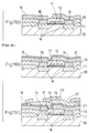
- FIGS. 1a - d illustrate in cross section subsequent steps of the fabrication of a semiconductor device according to a first embodiment of the present invention.
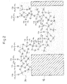
- FIG. 2 is a diagram cross-sectionally illustrating the structure of a molecular layer formed on a first metallization layer according to a method of the first embodiment.
- FIGS. 3a - c illustrate steps of the formation of a molecular layer in the first embodiment.
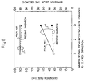
- FIG. 4 is a graph showing a way of obtaining the deposition rate and the deposition delay time to observe the dependence of the overlying layer on the underlying topography.
- FIG. 5 is a graph showing the relationships of the underlaying layer material versus the deposition rate and the deposition delay time.
- FIG. 6 is a graph showing the relationships of the elapsed time from the formation of a P-TEOS layer or molecular layer until the formation of a TEOS-O3 layer versus the deposition rate/deposition delay time.
- FIG. 7 is a graph showing differences in the surface roughness and in the number of pores between a conventionally formed TEOS-O3 layer and a TEOS-O3 layer of the first embodiment.
- FIG. 8 is a cross-sectional view in respect to the evaluation of both a conventionally formed TEOS-O3 layer and a TEOS-O3 layer of the first embodiment.
- FIGS. 9a - c illustrate in cross section subsequent steps of the fabrication of a semiconductor device according to a second embodiment of the present invention.
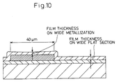
- FIG. 10 is a cross-sectional view in respect to the evaluation of both a conventionally formed TEOS-O3 layer and a TEOS-O3 layer of the second embodiment.
- FIGS. 11a - c illustrate in cross section subsequent steps of the fabrication of a semiconductor device according to a conventional fabrication method.
- FIG. 12 is a diagram cross-sectionally illustrating the structure of a P-TEOS layer formed on a first metallization layer by means of a conventional method.
- FIG. 13 is a diagram cross-sectionally illustrating the structure of a conventionally formed P-TEOS layer when exposed to a N2-gas plasma.
- FIG. 14 is another diagram cross-sectionally illustrating the structure of a conventionally formed P-TEOS layer when exposed to a N2-gas plasma.
- FIGS. 1a - d illustrate in cross section subsequent steps of the fabrication of a semiconductor device according to a first embodiment of the present invention.
- source (or drain) region 14 Formed on silicon semiconductor substrate 10 are source (or drain) region 14 , gate insulating layer 17 , LOCOS layer 11 , gate electrode 12 of polysilicon, BPSG layer 13 , source (or drain) electrode 15 made of tungsten, and first metallization layer 16 .
- P-TEOS layer 21 i.e., a first silicon oxide
- BPSG layer 13 is deposited on BPSG layer 13 as well as on first metallization layer 16 by means of a plasma CVD from a source gas of TEOS (see FIG. 1b ).
- Hexamethyldisilazane is supplied to form molecular layer 24 on P-TEOS layer 21 (reaction temperature: 130° C; HMDS flow rate: 5 sccm; pressure: 1 atm; and reaction time: 5 minutes) (see FIG. 1c ).
- TEOS-O3 layer 22 i.e., a second silicon oxide
- molecular layer 24 by means of an APCVD process making use of the reaction of TEOS with O3, and second metallization layer 23 is formed on TEOS-O3 layer 22 (see FIG. 1d ).
- First metallization layer 16 may be formed by such materials as silicon materials (e.g., crystal silicon and polycrystal silicon), silicon dioxide compounds (e.g., BPSG), and metallic materials (e.g., aluminum alloys, titanium compounds, tungsten compounds). Silicon material is readily oxidized, so a native oxide is created on the surface, and even TiN metal, which is very unlikely to be oxidized, becomes nonstoicheiometric and suffers from a Ti oxide on the surface layer.
- silicon materials e.g., crystal silicon and polycrystal silicon
- silicon dioxide compounds e.g., BPSG
- metallic materials e.g., aluminum alloys, titanium compounds, tungsten compounds.
- first metallization layer's 16 surface is covered with "-OH” groups, and if HMDS is supplied onto the surface of first metallization layer 16 , the HMDS thus supplied reacts with the "-OH” groups to form a water-hating or hydrophobic molecular layer.
- silylation reaction One method of producing hydrophobic molecular layer is a silylation process.
- a silylation compound such as HMDS reacts with "-OH” groups thereby replacing "H's" of the "-OH” groups with silyl groups to take a form of "-O-Si(CH3)3".
- Silylation reaction occurs at room temperature so that a silylation process can be carried out easily.
- Every existing dangling bond is covered with "Si-(CH3)3". This can prevent the dangling bond from exerting ill-effect on the deposition of TEOS-O3 layer 22 .
- molecular layer 24 composed of HMDS is formed on top of first metallization layer 16 and TEOS-O3 layer 22 is formed on molecular layer 24 .
- FIG. 4 is a graph showing a way of obtaining the deposition rate and the deposition delay time to observe the dependence of TEOS-O3 layer 22 on the underlying topography.
- FIG. 4 also shows the relationship of the deposited film thickness versus the deposition time, in the cases of the TEOS-O3-on-crystal silicon deposition and the TEOS-O3-on-P-TEOS deposition.
- the deposition delay time is the value obtained at a measurement point where extrapolation line shows that a deposited film thickness is zero, and the deposition rate is found from the extrapolation line's tilt angle.
- FIG. 5 shows the relationship of the underlying layer material versus the deposition rate/deposition delay time.
- Such samples as crystal silicon, P-TEOS, post-glass flow BPSG, and TiN were used, and each of the first three samples was kept in the clean room for three days from the sample preparation until the deposition of TEOS-O3 layer 22 on each sample.
- the TiN sample was likewise kept, but for 21 days. This examination showed that the crystal silicon proved to provide the fastest deposition rate, with the TiN, the P-TEOS, and the BPSG, in that order, and that the BPSG proved to produce the greatest deposition delay time, with the P-TEOS, the TiN, and the crystal silicon, in that order.
- the cause of the above results was investigated by changing the length of time taken from the formation of P-TEOS layer 21 until the deposition of TEOS-O3 layer 22 on P-TEOS layer 21 , to a period of one day and to a period of three days. Additionally, to evaluate the present invention, another testing was carried out by changing the length of time taken from the formation of molecular layer 24 on P-TEOS layer 21 until the deposition of TEOS-O3 layer 22 on molecular layer 24 , to a period of one day and to a period of three days.
- FIG. 6 shows the results. As seen from FIG. 6 , the deposition rate did not vary with time in both of the conventional technique case and the present invention case, but, as to the deposition delay time, there were found differences between them. For the case of the conventional technique, the deposition delay time increased with time, whereas, for the case of the present invention technique taking advantage of molecular layer 24 , the deposition delay time stayed unchanged.
- TEOS-O3 layer 22 If an underlying layer (i.e., P-TEOS layer 21 ) is covered with molecular layer 24 in prior to forming TEOS-O3 layer 22 , the surface of the underlaying layer becomes uniform and hydrophobic. This allows the APCVD method utilizing the chemical reaction of TEOS with O3 to deposit TEOS-O3 layer 22 having good film properties.
- TEOS-O3 layer 22 was formed and was forced to fracture. Then, the surface and inside of TEOS-O3 layer 22 was slightly etched using a water solution of hydrofluoric acid, and the surface roughness and the number of pores (i.e., the number of recesses) caused by the strength and weakness of etching were examined. Because of the existence of molecular layer 24 overlying P-TEOS layer 21 , the surface of TEOS-O3 layer 22 of the present invention suffers less severe surface roughness and a less number of pores, compared with the conventional technique.
- TEOS-O3 layer 22 A semiconductor device was cut after TEOS-O3 layer 22 had been formed, and the cross section thereof was observed using a scanning electron microscope (SEM). More specifically, as shown in FIG. 8 , the film thickness of TEOS-O3 layer 22 was measured at different locations, namely at a point overlying a metallization having a great width of 40 ⁇ m and at a point overlying a wide flat section with no metallizations provided, in order to find the ratio of the film thickness measured at the former point to the film thickness measured at the latter point.
- the present invention provided a ratio value of 0.99 versus 0.70 for the conventional technique.
- the prior art technique produces the problem in that the film thickness of TEOS-O3 layer 22 formed on a wide interconnection metallization is thinner than on a wide flat section containing no metallizations.
- the present invention provides a solution to such a problem.
- a first assumption is that P-TEOS layer 21 is raised locally by first metallization layer 16 , whereby the raised portion is exposed intensively to charges or particles from a plasma thereby causing the deterioration of P-TEOS layer 21 to occur.
- a second assumption is that part of P-TEOS layer 21 overlying first metallization layer 16 is very much influenced by thermal expansion of first metallization layer 16 thereby causing the deterioration of P-TEOS layer 21 to occur.
- FIGS. 9a - d a semiconductor device and associated fabrication method of a second embodiment of the present invention are described.
- source (or drain) region 14 Formed on semiconductor substrate 10 are source (or drain) region 14 , gate insulating layer 17 , LOCOS layer 11 , polysilicon gate electrode 12 , BPSG layer 13 , tungsten source (or drain) region 15 , and first metallization layer 16 (see FIG. 9a ).
- semiconductor substrate 10 is drip-fed an HMDS solution and is spin-coated with HMDS, and, as shown in FIG. 9b , HMDS molecular layer 24 is formed on first metallization layer 16 .
- TEOS-O3 layer 22 on molecular layer 24 .
- second metallization layer 23 on TEOS-O3 layer 22 (see FIG. 9c ).
- TEOS-O3 layer 22 was deposited on first metallization layer 16 without forming P-TEOS layer 21 but with an intervening molecular layer, in order to investigate the effect of silylation on the deposition of TEOS-O3 layer 22 .
- the profile of TEOS-O3 layer 22 thus formed was examined using an SEM in order to measure the film thickness of TEOS-O3 layer 22 at two locations, namely at a point overlying a 40 ⁇ m-wide metallization and at a point overlying a wide flat section with no metallizations provided.
- the ratio of the film thickness measured at the former point to that measured at the latter point was found.
- the present invention provided a ratio value of 0.96 versus 0.40 for the conventional technique. There were observed outstanding differences in the film thickness of TEOS-O3 layer 22 overlying a wide metallization.
- TEOS-O3 layer 22 decreases in film thickness in the vicinity of the center of the wide metallization layer down to about 40% of the film thickness of TEOS-O3 layer 22 overlying the flat section (see FIG. 10 ).
- the film thickness of TEOS-O3 layer 22 varies depending on the metallization pattern, resulting in causing capacitance variations between metallizations and causing throughhole depth variations.
- the present invention is able to provide conformal deposition because of the above-mentioned ratio value.
- TEOS-O3 layer 22 is deposited by means of APCVD.
- APCVD atomic layer deposition
- other deposition techniques such as simply depositing TEOS-O3 layer 22 in a reduced pressure state may be used with the same effect.
- the plasma CVD method to generate ozone by exposing oxygen to a plasma or UV light, or the photo CVD may be employed.
- aluminum alloy is used as metallization material.
- other functionally equivalent metallization materials such as pure aluminum and capper may be used with the same effect.
- HMDS is used to form molecular layer 24 .
- other surface-active agents including silane compounds, siloxane compounds, disilazane compounds, trisilazane compounds, piperazine compounds, aminogermanium compounds, halide germanium compounds, may be used.
- TEOS is used to form P-TEOS layer 21 and TEOS-O3 layer 22 .
- other functionally equivalent organo-silicon compounds including tetramethoxysilane, tetrapropoxysilane, hexamethyldisiloxane, tetramethylsilane, and tetraethylsilane, may be used.
- the underlying layer surface topography is made uniform by the molecular layer. This eliminates the need for forming silicon oxides thereby further eliminating the need for the N2-gas plasma process. In other words, the number of semiconductor device fabrication steps can be reduced. Especially, the gate insulating layer becomes free from any damage due to the N2-gas plasma process, and there are no constraints to the device miniaturization required by the larger-scale integration.
Landscapes
- Internal Circuitry In Semiconductor Integrated Circuit Devices (AREA)
- Formation Of Insulating Films (AREA)
Applications Claiming Priority (3)
| Application Number | Priority Date | Filing Date | Title |
|---|---|---|---|
| JP20795093 | 1993-08-23 | ||
| JP207950/93 | 1993-08-23 | ||
| JP5207950A JPH0766287A (ja) | 1993-08-23 | 1993-08-23 | 半導体装置及びその製造方法 |
Publications (3)
| Publication Number | Publication Date |
|---|---|
| EP0643421A2 true EP0643421A2 (de) | 1995-03-15 |
| EP0643421A3 EP0643421A3 (de) | 1995-05-24 |
| EP0643421B1 EP0643421B1 (de) | 2000-05-31 |
Family
ID=16548228
Family Applications (1)
| Application Number | Title | Priority Date | Filing Date |
|---|---|---|---|
| EP94112986A Expired - Lifetime EP0643421B1 (de) | 1993-08-23 | 1994-08-19 | Halbleiteranordnung und zugehörige Herstellungsmethode |
Country Status (6)
| Country | Link |
|---|---|
| US (2) | US5723909A (de) |
| EP (1) | EP0643421B1 (de) |
| JP (1) | JPH0766287A (de) |
| KR (1) | KR0136685B1 (de) |
| CN (1) | CN1050694C (de) |
| DE (1) | DE69424728T2 (de) |
Cited By (10)
| Publication number | Priority date | Publication date | Assignee | Title |
|---|---|---|---|---|
| EP0678913A1 (de) * | 1994-04-15 | 1995-10-25 | Matsushita Electric Industrial Co., Ltd. | Herstellungsverfahren für Mehrlager-Metallisierung |
| US5576247A (en) * | 1992-07-31 | 1996-11-19 | Matsushita Electric Industrial Co., Ltd. | Thin layer forming method wherein hydrophobic molecular layers preventing a BPSG layer from absorbing moisture |
| CN1056468C (zh) * | 1995-06-28 | 2000-09-13 | 现代电子产业株式会社 | 用于在半导体器件的诸金属布线之间形成绝缘薄膜的方法 |
| US6395651B1 (en) | 1998-07-07 | 2002-05-28 | Alliedsignal | Simplified process for producing nanoporous silica |
| US7678712B2 (en) | 2005-03-22 | 2010-03-16 | Honeywell International, Inc. | Vapor phase treatment of dielectric materials |
| US7709371B2 (en) | 2003-01-25 | 2010-05-04 | Honeywell International Inc. | Repairing damage to low-k dielectric materials using silylating agents |
| US7858294B2 (en) | 2000-06-23 | 2010-12-28 | Honeywell International Inc. | Method to restore hydrophobicity in dielectric films and materials |
| US7915181B2 (en) | 2003-01-25 | 2011-03-29 | Honeywell International Inc. | Repair and restoration of damaged dielectric materials and films |
| US7915159B2 (en) | 2004-09-15 | 2011-03-29 | Honeywell International Inc. | Treating agent materials |
| US10461406B2 (en) | 2017-01-23 | 2019-10-29 | Microsoft Technology Licensing, Llc | Loop antenna with integrated proximity sensing |
Families Citing this family (21)
| Publication number | Priority date | Publication date | Assignee | Title |
|---|---|---|---|---|
| US5942802A (en) * | 1995-10-09 | 1999-08-24 | Matsushita Electric Industrial Co., Ltd. | Semiconductor device and method of producing the same |
| JP2975917B2 (ja) * | 1998-02-06 | 1999-11-10 | 株式会社半導体プロセス研究所 | 半導体装置の製造方法及び半導体装置の製造装置 |
| JP3426494B2 (ja) | 1998-04-02 | 2003-07-14 | 沖電気工業株式会社 | 半導体装置の製造方法 |
| US6294473B1 (en) * | 1998-06-03 | 2001-09-25 | Rodel Holdings Inc. | Method of polishing substrates comprising silicon dioxide and composition relating thereto |
| JP3248492B2 (ja) * | 1998-08-14 | 2002-01-21 | 日本電気株式会社 | 半導体装置及びその製造方法 |
| US6245690B1 (en) * | 1998-11-04 | 2001-06-12 | Applied Materials, Inc. | Method of improving moisture resistance of low dielectric constant films |
| US6090707A (en) * | 1999-09-02 | 2000-07-18 | Micron Technology, Inc. | Method of forming a conductive silicide layer on a silicon comprising substrate and method of forming a conductive silicide contact |
| US6449132B1 (en) | 1999-10-05 | 2002-09-10 | Seagate Technology Llc | Dielectric gap material for magnetoresistive heads with conformal step coverage |
| US6576980B1 (en) | 1999-11-30 | 2003-06-10 | Agere Systems, Inc. | Surface treatment anneal of hydrogenated silicon-oxy-carbide dielectric layer |
| US6674140B2 (en) | 2000-02-01 | 2004-01-06 | Analog Devices, Inc. | Process for wafer level treatment to reduce stiction and passivate micromachined surfaces and compounds used therefor |
| JP3944487B2 (ja) * | 2000-04-11 | 2007-07-11 | 松下電器産業株式会社 | 半導体装置の製造装置 |
| RU2193255C1 (ru) * | 2002-01-08 | 2002-11-20 | Санкт-Петербургский государственный электротехнический университет | Микроэлектронная структура на основе "кремний-диэлектрик" для изготовления полупроводниковых приборов и способ ее получения |
| JP2006502539A (ja) * | 2002-10-07 | 2006-01-19 | コーニンクレッカ フィリップス エレクトロニクス エヌ ヴィ | 発光ディスプレイの製造方法 |
| US20040145030A1 (en) * | 2003-01-28 | 2004-07-29 | Meagley Robert P. | Forming semiconductor structures |
| JP4588304B2 (ja) * | 2003-08-12 | 2010-12-01 | Azエレクトロニックマテリアルズ株式会社 | コーティング組成物、およびそれを用いて製造した低誘電シリカ質材料 |
| US7500397B2 (en) | 2007-02-15 | 2009-03-10 | Air Products And Chemicals, Inc. | Activated chemical process for enhancing material properties of dielectric films |
| WO2010064306A1 (ja) * | 2008-12-03 | 2010-06-10 | 富士通株式会社 | 半導体装置の製造方法 |
| CN102487004A (zh) * | 2010-12-01 | 2012-06-06 | 中芯国际集成电路制造(上海)有限公司 | 利用化学气相淀积填充隔离槽的方法 |
| CN103871961B (zh) * | 2012-12-17 | 2017-08-25 | 中芯国际集成电路制造(上海)有限公司 | 互连结构及其制造方法 |
| US8871639B2 (en) | 2013-01-04 | 2014-10-28 | Taiwan Semiconductor Manufacturing Company, Ltd. | Semiconductor devices and methods of manufacture thereof |
| CN114400234B (zh) * | 2021-12-17 | 2025-02-25 | 武汉新芯集成电路股份有限公司 | 背照式影像传感器芯片及其制作方法 |
Family Cites Families (8)
| Publication number | Priority date | Publication date | Assignee | Title |
|---|---|---|---|---|
| US4885262A (en) * | 1989-03-08 | 1989-12-05 | Intel Corporation | Chemical modification of spin-on glass for improved performance in IC fabrication |
| DE3933908A1 (de) * | 1989-10-11 | 1991-04-25 | Telefunken Electronic Gmbh | Verfahren zur herstellung einer integrierten mos-halbleiteranordnung |
| JPH03152957A (ja) * | 1989-11-09 | 1991-06-28 | Sony Corp | 半導体装置の製造方法 |
| DE4135810C2 (de) * | 1990-10-30 | 2000-04-13 | Mitsubishi Electric Corp | Halbleitereinrichtung mit einem Zwischenschichtisolierfilm und Verfahren zu deren Herstellung |
| JP2640174B2 (ja) * | 1990-10-30 | 1997-08-13 | 三菱電機株式会社 | 半導体装置およびその製造方法 |
| US5219791A (en) * | 1991-06-07 | 1993-06-15 | Intel Corporation | TEOS intermetal dielectric preclean for VIA formation |
| EP0560617A3 (en) * | 1992-03-13 | 1993-11-24 | Kawasaki Steel Co | Method of manufacturing insulating film on semiconductor device and apparatus for carrying out the same |
| US5576247A (en) * | 1992-07-31 | 1996-11-19 | Matsushita Electric Industrial Co., Ltd. | Thin layer forming method wherein hydrophobic molecular layers preventing a BPSG layer from absorbing moisture |
-
1993
- 1993-08-23 JP JP5207950A patent/JPH0766287A/ja active Pending
-
1994
- 1994-08-10 KR KR94019713A patent/KR0136685B1/ko not_active Expired - Fee Related
- 1994-08-19 EP EP94112986A patent/EP0643421B1/de not_active Expired - Lifetime
- 1994-08-19 DE DE69424728T patent/DE69424728T2/de not_active Expired - Fee Related
- 1994-08-22 CN CN94115769A patent/CN1050694C/zh not_active Expired - Fee Related
-
1996
- 1996-09-11 US US08/712,237 patent/US5723909A/en not_active Expired - Fee Related
-
1997
- 1997-07-07 US US08/888,919 patent/US5950101A/en not_active Expired - Fee Related
Cited By (13)
| Publication number | Priority date | Publication date | Assignee | Title |
|---|---|---|---|---|
| US5576247A (en) * | 1992-07-31 | 1996-11-19 | Matsushita Electric Industrial Co., Ltd. | Thin layer forming method wherein hydrophobic molecular layers preventing a BPSG layer from absorbing moisture |
| EP0678913A1 (de) * | 1994-04-15 | 1995-10-25 | Matsushita Electric Industrial Co., Ltd. | Herstellungsverfahren für Mehrlager-Metallisierung |
| CN1056468C (zh) * | 1995-06-28 | 2000-09-13 | 现代电子产业株式会社 | 用于在半导体器件的诸金属布线之间形成绝缘薄膜的方法 |
| US6395651B1 (en) | 1998-07-07 | 2002-05-28 | Alliedsignal | Simplified process for producing nanoporous silica |
| US6495906B2 (en) | 1998-07-07 | 2002-12-17 | Alliedsignal Inc. | Simplified process for producing nanoporous silica |
| WO2000002233A3 (en) * | 1998-07-07 | 2003-04-17 | Allied Signal Inc | Simplified process for producing nanoporous silica |
| US7858294B2 (en) | 2000-06-23 | 2010-12-28 | Honeywell International Inc. | Method to restore hydrophobicity in dielectric films and materials |
| US8440388B2 (en) | 2000-06-23 | 2013-05-14 | Honeywell International Inc. | Method to restore hydrophobicity in dielectric films and materials |
| US7915181B2 (en) | 2003-01-25 | 2011-03-29 | Honeywell International Inc. | Repair and restoration of damaged dielectric materials and films |
| US7709371B2 (en) | 2003-01-25 | 2010-05-04 | Honeywell International Inc. | Repairing damage to low-k dielectric materials using silylating agents |
| US7915159B2 (en) | 2004-09-15 | 2011-03-29 | Honeywell International Inc. | Treating agent materials |
| US7678712B2 (en) | 2005-03-22 | 2010-03-16 | Honeywell International, Inc. | Vapor phase treatment of dielectric materials |
| US10461406B2 (en) | 2017-01-23 | 2019-10-29 | Microsoft Technology Licensing, Llc | Loop antenna with integrated proximity sensing |
Also Published As
| Publication number | Publication date |
|---|---|
| DE69424728D1 (de) | 2000-07-06 |
| DE69424728T2 (de) | 2000-09-28 |
| CN1050694C (zh) | 2000-03-22 |
| KR950007023A (ko) | 1995-03-21 |
| EP0643421B1 (de) | 2000-05-31 |
| JPH0766287A (ja) | 1995-03-10 |
| KR0136685B1 (en) | 1998-04-29 |
| US5950101A (en) | 1999-09-07 |
| US5723909A (en) | 1998-03-03 |
| EP0643421A3 (de) | 1995-05-24 |
| CN1109216A (zh) | 1995-09-27 |
Similar Documents
| Publication | Publication Date | Title |
|---|---|---|
| EP0643421B1 (de) | Halbleiteranordnung und zugehörige Herstellungsmethode | |
| US5840631A (en) | Method of manufacturing semiconductor device | |
| US6124641A (en) | Semiconductor device organic insulator film | |
| US6426015B1 (en) | Method of reducing undesired etching of insulation due to elevated boron concentrations | |
| US5703404A (en) | Semiconductor device comprising an SiOF insulative film | |
| KR0184279B1 (ko) | 금속 또는 금속실리사이드막의 형성방법 | |
| US6127256A (en) | Semiconductor device and method of manufacturing the same | |
| KR100368504B1 (ko) | 반도체장치제조방법 | |
| US6187662B1 (en) | Semiconductor device with low permittivity interlayer insulating film and method of manufacturing the same | |
| US4732801A (en) | Graded oxide/nitride via structure and method of fabrication therefor | |
| US20010004550A1 (en) | Damascene-type interconnection structure and its production process | |
| EP0434045B1 (de) | Verfahren zum selektiven Herstellen von leitendem Stoff | |
| US7067416B2 (en) | Method of forming a conductive contact | |
| CN100352035C (zh) | 用于高纵横比半导体器件的掺硼氮化钛层 | |
| US6791149B2 (en) | Diffusion barrier layer for semiconductor wafer fabrication | |
| US5869394A (en) | Teos-ozone planarization process | |
| JP3789501B2 (ja) | 半導体装置に用いられる絶縁膜構造の製造方法 | |
| KR0149468B1 (ko) | 반도체 장치의 제조방법 | |
| JPH0697163A (ja) | 薄膜形成方法及び半導体装置の製造方法 | |
| JPH07122552A (ja) | 半導体装置における絶縁膜形成方法 | |
| Obeng et al. | Dielectric materials for advanced VLSI and ULSI technologies | |
| JP2629587B2 (ja) | 半導体装置の製造方法 | |
| JPH05243213A (ja) | 半導体装置の製造方法 | |
| JPH07273193A (ja) | 半導体装置及びその製造方法 | |
| JP2000216157A (ja) | ケミカルメカニカルポリシング処理およびこれを用いた金属のインタ―コネクトを形成する方法 |
Legal Events
| Date | Code | Title | Description |
|---|---|---|---|
| PUAI | Public reference made under article 153(3) epc to a published international application that has entered the european phase |
Free format text: ORIGINAL CODE: 0009012 |
|
| AK | Designated contracting states |
Kind code of ref document: A2 Designated state(s): DE FR GB NL |
|
| PUAL | Search report despatched |
Free format text: ORIGINAL CODE: 0009013 |
|
| AK | Designated contracting states |
Kind code of ref document: A3 Designated state(s): DE FR GB NL |
|
| 17P | Request for examination filed |
Effective date: 19950817 |
|
| 17Q | First examination report despatched |
Effective date: 19961211 |
|
| GRAG | Despatch of communication of intention to grant |
Free format text: ORIGINAL CODE: EPIDOS AGRA |
|
| GRAG | Despatch of communication of intention to grant |
Free format text: ORIGINAL CODE: EPIDOS AGRA |
|
| GRAH | Despatch of communication of intention to grant a patent |
Free format text: ORIGINAL CODE: EPIDOS IGRA |
|
| GRAH | Despatch of communication of intention to grant a patent |
Free format text: ORIGINAL CODE: EPIDOS IGRA |
|
| GRAA | (expected) grant |
Free format text: ORIGINAL CODE: 0009210 |
|
| AK | Designated contracting states |
Kind code of ref document: B1 Designated state(s): DE FR GB NL |
|
| REF | Corresponds to: |
Ref document number: 69424728 Country of ref document: DE Date of ref document: 20000706 |
|
| ET | Fr: translation filed | ||
| PLBE | No opposition filed within time limit |
Free format text: ORIGINAL CODE: 0009261 |
|
| STAA | Information on the status of an ep patent application or granted ep patent |
Free format text: STATUS: NO OPPOSITION FILED WITHIN TIME LIMIT |
|
| 26N | No opposition filed | ||
| REG | Reference to a national code |
Ref country code: GB Ref legal event code: IF02 |
|
| PGFP | Annual fee paid to national office [announced via postgrant information from national office to epo] |
Ref country code: FR Payment date: 20050809 Year of fee payment: 12 |
|
| PGFP | Annual fee paid to national office [announced via postgrant information from national office to epo] |
Ref country code: DE Payment date: 20050811 Year of fee payment: 12 |
|
| PGFP | Annual fee paid to national office [announced via postgrant information from national office to epo] |
Ref country code: NL Payment date: 20050815 Year of fee payment: 12 |
|
| PGFP | Annual fee paid to national office [announced via postgrant information from national office to epo] |
Ref country code: GB Payment date: 20050817 Year of fee payment: 12 |
|
| PG25 | Lapsed in a contracting state [announced via postgrant information from national office to epo] |
Ref country code: NL Free format text: LAPSE BECAUSE OF NON-PAYMENT OF DUE FEES Effective date: 20070301 Ref country code: DE Free format text: LAPSE BECAUSE OF NON-PAYMENT OF DUE FEES Effective date: 20070301 |
|
| GBPC | Gb: european patent ceased through non-payment of renewal fee |
Effective date: 20060819 |
|
| NLV4 | Nl: lapsed or anulled due to non-payment of the annual fee |
Effective date: 20070301 |
|
| REG | Reference to a national code |
Ref country code: FR Ref legal event code: ST Effective date: 20070430 |
|
| PG25 | Lapsed in a contracting state [announced via postgrant information from national office to epo] |
Ref country code: GB Free format text: LAPSE BECAUSE OF NON-PAYMENT OF DUE FEES Effective date: 20060819 |
|
| PG25 | Lapsed in a contracting state [announced via postgrant information from national office to epo] |
Ref country code: FR Free format text: LAPSE BECAUSE OF NON-PAYMENT OF DUE FEES Effective date: 20060831 |