EP0643423B1 - Dispositif semi-conducteur en diamant - Google Patents
Dispositif semi-conducteur en diamant Download PDFInfo
- Publication number
- EP0643423B1 EP0643423B1 EP94113945A EP94113945A EP0643423B1 EP 0643423 B1 EP0643423 B1 EP 0643423B1 EP 94113945 A EP94113945 A EP 94113945A EP 94113945 A EP94113945 A EP 94113945A EP 0643423 B1 EP0643423 B1 EP 0643423B1
- Authority
- EP
- European Patent Office
- Prior art keywords
- type
- diamond
- layer
- type layer
- semiconductor device
- Prior art date
- Legal status (The legal status is an assumption and is not a legal conclusion. Google has not performed a legal analysis and makes no representation as to the accuracy of the status listed.)
- Expired - Lifetime
Links
Images










Classifications
-
- H—ELECTRICITY
- H10—SEMICONDUCTOR DEVICES; ELECTRIC SOLID-STATE DEVICES NOT OTHERWISE PROVIDED FOR
- H10D—INORGANIC ELECTRIC SEMICONDUCTOR DEVICES
- H10D62/00—Semiconductor bodies, or regions thereof, of devices having potential barriers
- H10D62/80—Semiconductor bodies, or regions thereof, of devices having potential barriers characterised by the materials
- H10D62/83—Semiconductor bodies, or regions thereof, of devices having potential barriers characterised by the materials being Group IV materials, e.g. B-doped Si or undoped Ge
- H10D62/8303—Diamond
-
- H—ELECTRICITY
- H10—SEMICONDUCTOR DEVICES; ELECTRIC SOLID-STATE DEVICES NOT OTHERWISE PROVIDED FOR
- H10D—INORGANIC ELECTRIC SEMICONDUCTOR DEVICES
- H10D18/00—Thyristors
-
- H—ELECTRICITY
- H10—SEMICONDUCTOR DEVICES; ELECTRIC SOLID-STATE DEVICES NOT OTHERWISE PROVIDED FOR
- H10D—INORGANIC ELECTRIC SEMICONDUCTOR DEVICES
- H10D30/00—Field-effect transistors [FET]
- H10D30/202—FETs having static field-induced regions, e.g. static-induction transistors [SIT] or permeable base transistors [PBT]
-
- Y—GENERAL TAGGING OF NEW TECHNOLOGICAL DEVELOPMENTS; GENERAL TAGGING OF CROSS-SECTIONAL TECHNOLOGIES SPANNING OVER SEVERAL SECTIONS OF THE IPC; TECHNICAL SUBJECTS COVERED BY FORMER USPC CROSS-REFERENCE ART COLLECTIONS [XRACs] AND DIGESTS
- Y02—TECHNOLOGIES OR APPLICATIONS FOR MITIGATION OR ADAPTATION AGAINST CLIMATE CHANGE
- Y02E—REDUCTION OF GREENHOUSE GAS [GHG] EMISSIONS, RELATED TO ENERGY GENERATION, TRANSMISSION OR DISTRIBUTION
- Y02E10/00—Energy generation through renewable energy sources
- Y02E10/50—Photovoltaic [PV] energy
- Y02E10/548—Amorphous silicon PV cells
Definitions
- the present invention relates to a diamond semiconductor device which is formed as a diode, a transistor, or other semiconductor devices using various conduction type dopant doped diamond as a semiconductor material.
- Diamond is doped with III-element or V-element, which results in p-type semiconductor or n-type semiconductor, respectively. Further, diamond has a large energy gap of about 5.5eV, which means that an intrinsic region, at which carrier movement is uncontrollable, is not present below 1400°C. Therefore, with use of diamond as semiconductor, a semiconductor device which is stable thermally, that is, a semiconductor device which can operate at high temperature may be formed.
- Diamond is stable chemically and has a heat conductivity of 20 W/cm ⁇ K which is ten times larger than that of silicon and is superior in heat radiation. Further, diamond has a small permitivity of 5.5, a large breakdown voltage of 5x10 6 V/cm and a large carrier mobility; an electron mobility of 2000cm 2 /V ⁇ s and a hole mobility of 2100cm 2 /V ⁇ s at 300K. Therefore, the diamond semiconductor is also expected to be used at high frequency and high output power.
- Document EP 0 445 998 A1 discloses diamond semiconductor devices wherein a non-doped or low-doped diamond layer with high resistivity is epitaxially grown between the n-type diamond layer and the p-type diamond layer in the pn junction diode or between the metal layer and the doped diamond layer in the Schottky diode.
- Patent abstracts of Japan, vol. 17, no. 110, 8 March 1993 and JP-A-4-293 272 disclose a diamond P-I-N diode with an n-type Si-doped diamond semiconductor layer, a non-doped diamond insulating layer and a p-type B-doped diamond semiconductor layer which are formed in order on a n-type Si substrate of a low resistance using a microwave CVD method.
- This disclosure is not directed to a diamond semiconductor device with a n-type diamond layer wherein ist n-type dopant is nitrogen.
- a dopant to be doped to diamond is limited to an atom having a small radius such as boron, nitrogen or the like. Therefore, the conventional diamond semiconductor device has a problem that the metal conduction dominates in pn junction, which makes the control of carriers harder. Accordingly, the diamond semiconductor device which practically operates as a pn junction diode, a pnp junction transistor or an npn junction transistor has not been manufactured.
- an object of the present invention is to provide a diamond semiconductor device which has diode characteristics.
- a diamond semiconductor device of the present invention comprises an n-type diamond layer to which an n-type dopant is doped at high concentration so that metal conduction dominates, a p-type diamond layer to which a p-type dopant is doped at high concentration so that metal conduction dominates, and a high resistance diamond layer formed between the n-type diamond layer and the p-type diamond layer, wherein the n-type dopant of the n-type diamond layer is 10 17 cm -3 or above, so that metal conduction dominates in the n-type diamond layer.
- the thickness and the doping concentration of the high resistance diamond layer are values at which semiconductor conduction dominates between the n-type diamond layer and the p-type diamond layer.
- the nitrogen concentration of the n-type diamond layer is 1x10 19 cm -3 or above, and that the nitrogen concentration of the high resistance diamond layer is less than 1x10 17 cm -3 .
- the p-type dopant is preferably boron.
- the boron concentration of the p-type diamond layer is 1x10 17 cm -3 or above, and that the boron concentration of the high resistance diamond layer is less than 1x10 17 cm -3 .
- the boron concentration of the p-type diamond layer is 1x10 19 cm -3 or above, and that the boron concentration of the high resistance diamond layer is less than 1x10 19 cm -3 .
- the thickness of the high resistance diamond layer is preferably within a range of 30-3000nm.
- the n-type diamond layer and the p-type diamond layer are formed by doping an n-type dopant and a p-type dopant at high concentration, respectively, so that the donor level and the acceptor level degenerate and are present near the conduction band and the valance band, respectively. Therefore, metal conduction dominates as carrier conduction.
- the inventors of the present application thought that as the thickness and the doping concentration of the high registance diamond layer, which is formed between the n-type diamond layer and the p-type diamond layer, were set to predetermined values, semiconductor conduction dominated in pn junction and the control of carriers was possible.
- an applied voltage is forward bias
- electrons are injected from the n-type diamond layer to the p-type diamond layer through the conduction band of the high resistance diamond layer
- holes are injected from the p-type diamond layer to the n-type diamond layer through the valance band of the high resistance diamond layer, so that a current flows.
- the applied voltage is reverse bias
- the dopant is doped to the high resistance diamond layer at low concentration or substantially no dopant is doped thereto, carriers are rarely present, so that a large current does not flow.
- semiconductor conduction dominates in pn junction as carrier conduction because of the large reverse withstand voltage, so that the rectification can be obtained. Accordingly, semiconductor conduction dominates in pn junction and carriers can be controlled, so that good diode characteristics or transistor characteristics can be achieved.
- Fig. 1 is a graph showing an energy diagram to explain pn junction of a diamond semiconductor not comprising a high resistance diamond layer.
- Fig. 2 is a graph showing an energy diagram to explain pn junction of a diamond semiconductor comprising a high resistance diamond layer in a diamond semiconductor device of the present invention.
- Fig. 3 is a graph showing the distribution of a doping concentration in pn junction of a diamond semiconductor in a case that a thickness of a high resistance diamond layer is very small and that an n-type doping concentration N A and a p-type doping concentration N D are substantially zero.
- Fig.4 is a graph showing an energy diagram corresponding to the distribution of a doping concentration of Fig. 3.
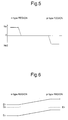
- Fig. 5 is a graph showing the distribution of a doping concentration in pn junction of a diamond semiconductor in a case that a thickness of a high resistance diamond layer is very large and larger than a mean free path of an electron or a hole, and that an n-type doping concentration N A and a p-type doping concentration N D are substantially zero.
- Fig. 6 is a graph showing an energy diagram corresponding to the distribution of a doping concentration of Fig. 5.
- Fig. 7 is a graph showing the distribution of a doping concentration in pn junction of a diamond semiconductor in a case that a thickness of a high resistance diamond layer is within a predetermined range, and that an n-type dopant and a p-type dopant are both doped to the high resistance diamond layer and an n-type doping concentration N A and a p-type doping concentration N D gradually decrease from an n-type diamond layer side or a p-type diamond layer side.
- Fig. 8 is a graph showing an energy diagram corresponding to the distribution of a doping concentration of Fig. 7.
- Fig. 9 is a graph showing the distribution of a doping concentration in pn junction of a diamond semiconductor in a case that a thickness of a high resistance diamond layer is within a predetermined range, and that two inclining doping regions in which an n-type doping concentration N A and a p-type doping concentration N D gradually decrease from an n-type diamond layer side or a p-type diamond layer side are formed although both an n-type dopant and a p-type dopant are not partially doped to the high resistance diamond layer.
- Fig. 10 is a graph showing an energy diagram corresponding to the distribution of a doping concentration of Fig. 9.
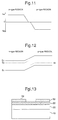
- Fig. 11 is a graph showing the distribution of a doping concentration in pn junction of a diamond semiconductor in a case that a thickness of a high resistance diamond layer is within a predetermined range, and that a central non-doped region in which both an n-type dopant and a p-type dopant are not doped is formed and two inclining doping regions in which an n-type doping concentration concentration N A and a p-type doping concentration N D gradually decreases from an n-type diamond layer side or a p-type diamond layer side are formed although both an n-type dopant and a p-type dopant are not partially doped to the high resistance diamond layer.
- Fig. 12 is a graph showing an energy diagram corresponding to the distribution of a doping concentration of Fig. 11.
- Fig. 13 is a sectional view showing the structure of a diamond semiconductor device according to the preparation example of the present invention.
- Fig. 14 is a sectional view showing the structure of a diamond semiconductor device according to the comparative example of the present invention.
- Fig. 15 is a sectional view showing the structure of a diamond semiconductor device according to the first embodiment of the present invention.
- Fig. 16 is a sectional view showing the structure of a diamond semiconductor device according to the second embodiment of the present invention.
- Fig. 17 is a sectional view showing the structure of a diamond semiconductor device according to the third embodiment of the present invention.
- Fig. 18 is a sectional view showing the structure of a diamond semiconductor device according to the fourth embodiment of the present invention.
- Fig. 19 is a graph showing a transistor characteristic of a diamond semiconductor device of Fig. 18 that is a relation between a collector voltage and a collector current with a base current as a parameter.
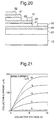
- Fig. 20 is a sectional view showing the structure of a diamond semiconductor device according the fifth embodiment of the present invention.
- Fig. 21 is a graph showing a transistor characteristic of a diamond semiconductor device of Fig. 20 that is a relation between a collector voltage and a collector current with a base current as a parameter.
- Fig. 22 is a sectional view showing the structure of a diamond semiconductor device according to the sixth embodiment of the present invention.
- Fig. 23 is a sectional view showing the structure along the lines B-B of Fig. 22.
- Fig. 24 is a graph showing a transistor characteristic of a diamond semiconductor device of Fig. 22 that is a relation between a drain voltage and a drain current with a gate voltage as a parameter.
- Fig. 25 is a sectional view showing the structure of a diamond semiconductor device according to the seventh embodiment of the present invention.
- Fig. 26 is a sectional view showing the structure along the lines B-B of Fig. 25.
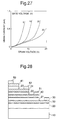
- Fig. 27 is a graph showing a transistor characteristic of a diamond semiconductor device of Fig. 25 that is a relation between a drain voltage and a drain current with a gate voltage as a parameter.
- Fig. 28 is a sectional view showing the structure of a diamond semiconductor device according to the eighth embodiment of the present invention.
- Fig. 29 is a graph showing a thyristor characteristic of a diamond semiconductor device of Fig. 28 that is a relation between a diamond semiconductor device in a drain voltage and a drain current in a case of a constant gate voltage.
- Fig. 30 is a sectional view showing the structure of a diamond semiconductor device according to the ninth embodiment of the present invention.
- Fig. 31 is a graph showing a thyristor characteristic of a diamond semiconductor device of Fig. 30 that is a relation between a drain voltage and a drain current in a case of a constant gate voltage.
- Fig. 1 is an energy diagram to explain pn junction of a diamond semiconductor not comprising a high resistance diamond layer.
- Fig. 1 shows a state of thermal equilibrium with a zero applied voltage in which an n-type diamond layer is directly coupled with a p-type diamond layer.
- a donor level E N measured from a conduction band E C is about 1-2eV, which is very deep.
- an acceptor level E P measured from a valence band E V is 0.37eV, which is shallow compared with the donor level E N .
- an applied voltage In a case that an applied voltage is forward bias, electrons are injected from the n-type region to the p-type region, and holes are injected from the p-type region to the n-type region, so that a current flows.
- an applied voltage is reverse bias, tunnel effect through the donor level E N and the acceptor level E P or avalanche occurs due to the high electric field generated near the pn junction, so that a large current flows.
- metal conduction dominates as carrier conduction in pn junction and rectification cannot be obtained, since a reverse withstand voltage has become small.
- the n-type diamond layer and the p-type diamond layer are formed by doping an n-type dopant and a p-type dopant at high concentration, respectively, so that the donor level and the acceptor level degenerate and are present around the conduction band and the valence band. Consequently, metal conduction dominates as carrier conduction. Further, a high resistance diamond layer having a predetermined thickness and a predetermined doping concentration is formed between the n-type diamond layer and the p-type diamond layer.
- Fig. 2 is an energy diagram to explain a pn junction of a diamond semiconductor having a high resistance diamond layer in a diamond semiconductor device of the present invention.
- the n-type diamond layer and the p-type diamond layer sandwiching the high resistance diamond layer and a state of thermal equilibrium, with a zero applied voltage are shown.
- an applied voltage In a case that an applied voltage is forward bias, electrons are injected from the p-type region into the p-type region through the conduction band which is a high resistance region, and the holes are injected from the p-type region to the n-type region through the valence band which is a high resistance region, so that a current flows.
- an applied voltage is reverse bias, carriers are rarely present in the high resistance diamond layer since the high resistance diamond layer has a low doping concentration, or has no doping concentration; consequently, a large current does not flow.
- semiconductor conduction dominates in pn junction as carrier conduction and rectification can be obtained, since the reverse withstand voltage has become large. Accordingly, semiconductor conduction dominates in pn junction to control carriers, so that excellent diode characteristics or transistor characteristics can be achieved.
- Fig. 3, Fig. 5, Fig. 7, Fig. 9 and Fig. 11 are graphs each showing the distribution of a doping concentration in pn junction of a diamond semiconductor having a high resistance diamond layer.
- Fig. 4, Fig. 6, Fig. 8, Fig. 10 and Fig. 12 are energy diagrams corresponding to the distribution of a doping concentration shown in the preceding figure.
- the region near pn junction becomes high resistance against a forward biasing voltage. Consequently, a current does not flow both the forward direction and the reverse direction, that is, this pn junction does not have the rectification.
- a thickness of a high resistance diamond layer is within a predetermined range, and that an n-type dopant and a p-type dopant are both doped to the high resistance diamond layer and the n-type doping concentration N A and the p-type doping concentration N D gradually decreases from an n-type diamond layer side or a p-type diamond layer side, the pn junction becomes pn junction of a diamond semiconductor device of the present invention. Therefore, because of the above reasons, the rectification can be obtained.
- the pn junction becomes pn junction of a diamond semiconductor device of the present invention. Therefore, because of the above reasons, the rectification can be obtained.
- the pn junction becomes pn junction of a diamond semiconductor device of the present invention. Therefore, because of the above reasons, the rectification can be obtained.
- Fig. 13 shows a cross section of the structure of a diamond semiconductor device according to the preparative example of the present invention.
- Electrode layers 50 and 51 are grown selectively on a part of the exposed surface of the n-type layer 30.
- the substrate 10 is an insulating substrate made of artificial monocrystalline diamond (Ib type) synthesized by high pressure or a semiconductor substrate made of silicon.
- the i-type layer 20 is deposited on the substrate 10 at a temperature of about 850°C and a pressure of 40 Torr while microwave having an output power of 300W is applied to a mixed gas containing H 2 of 100 sccm flow rate and CH 4 of 6 sccm flow rate to discharge at high frequency.
- the i-type layer 20 is made of high resistance diamond and has a thickness of about 2 ⁇ m.
- the n-type layer 30 is formed under the same condition as the i-type layer 20 with 7 sccm flow rate NH 3 added to the mixed gas.
- the n-type layer 30 is made of low resistance diamond and has a thickness of about 1 ⁇ m and nitrogen concentration of 1x10 17 cm -3 or above, preferably 1x10 19 cm -3 or above.
- electrode layers 50 and 51 are made of Ti/Mo/Au.
- the nitrogen concentration and the boron concentration are less than the nitrogen concentration of the n-type layer 30, and that the distribution of nitrogen and boron does not have to be uniform in a direction of the thickness.
- the n-type layer 30 is formed by doping nitrogen as an n-type dopant at high concentration, so that the donor level degenerates and are present near the conduction band. Therefore, metal conduction dominates as carrier conduction, so that the low resistance conductivity can be obtained at room temperature.
- the conductivity was measured.
- the resistivity detected was greater than 10 10 ⁇ cm, which was enormous to be specified, as a result of this measurementment.
- the conductivity was measured.
- the hole effect was detected, which meant that the carriers were electrons, and the conduction type of the n-type layer 30 made of nitrogen doped diamond was confirmed, as a result of this measurementment.
- the i-type layer 20 and the n-type layer 30 were made of monocrystalline diamond semiconductor formed on a monocrystalline diamond substrate and in the case that they were made of polycrystalline diamond semiconductor formed on a silicon substrate, the same results were obtained.
- Fig. 14 is a sectional view showing a diamond semiconductor device according to the comparative example of the present invention.
- a p-type layer 40 and an n-type layer 30 are deposited on a substrate 10 in order by a microplasma CVD method.
- the n-type layer 30 is grown selectively on a predetermined position of the exposed surface of the p-type layer 40.
- electrode layers 50 and 51 are grown selectively on a part of the exposed surface of the p-type layer 40 and the n-type layer 30, respectively.
- the substrate 10, the n-type layer 30 and the electrode layers 50 and 51 are formed under the same condition as the preparative example, but the p-type layer 40 is formed under the same condition as the n-type layer 30 but NH 3 added to the mixed gas is replaced with B 2 H 6 of 2sccm flow rate (hydrogen dilution: 1000 ppm).
- the p-type layer 40 is made of low resistance diamond and has a thickness of about 1 ⁇ m and a boron concentration of 1x10 17 cm -3 or above, preferably 1x10 19 cm -3 or above.
- the n-type layer 30 and the p-type layer 40 are formed by doping nitrogen and boron as an n-type dopant and a p-type dopant at high concentration, respectively, so that the donor level and the acceptor level degenerate and are present near the conduction band and the valence band, respectively. Therefore, metal conduction dominates as carrier conduction, so that the low resistance conductivity can be obtained even at room temperature.
- the carrier conduction is not controlled, so that the diamond semiconductor device can not obtain the diode characteristics as a semiconductor device constituting a two-terminal diode.
- the diamond semiconductor device was formed in the same manner as the comparative example except the nitrogen concentration of the n-type layer 30 being varied in a certain range, and the electrical characteristics were measured.
- the change in the rectification ratio corresponding to the nitrogen concentration from 1x10 17 cm -3 to 1x10 19 cm -3 of the n-type layer 30 is shown in Table 1.
- the recification ratio represents a ratio I S /I V of a forward current I S to a reverse current I V corresponding to a applied voltage of 10V.
- the p-type layer 40 and the n-type layer 30 were made of monocrystalline diamond semiconductor formed on a monocrystalline diamond substrate and in the case that they were made of polycrystalline diamond semiconductor formed on a silicon substrate, the same results were obtained.
- Fig. 15 is a sectional view showing the structure of a diamond semiconductor device according to the first embodiment of the present invention.
- An i-type layer 20, an n-type layer 30, an i-type layer 21 and a p-type layer 40 are deposited on a substrate 10 in order by a microplasma CVD method.
- the i-type layer 21 is grown selectively on a predetermined position of the exposed surface of the n-type layer 30.
- the p-type layer 40 is grown selectively on a predetermined position of the exposed surface of the i-type layer 21.
- electrode layers 50 and 51 are grown selectively on a part of the exposed surface of the n-type layer 30 and the p-type layer 40, respectively.
- the substrate 10, the i-type layer 20, the n-type layer 30 and the electrode layers 50 and 51 are formed under substantially the same condition as the preparative example, but the i-type layer 21 is formed under the same condition as the i-type layer 20, and the i-type layer 21 is made of high resistance diamond and has a thickness of 0.2-1 ⁇ m.
- the p-type layer 40 is formed under the same condition as the i-type layer 20, with B 2 H 6 of 2sccm flow rate (hydrogen dilution: 1000 ppm) added to mixed gas.
- the p-type layer 40 is made of low resistance diamond and has a thickness of about 1 ⁇ m and a boron concentration of 1x10 17 cm -3 or above, preferably 1x10 19 cm -3 or above.
- the nitrogen concentration and the boron concentration are less than the nitrogen concentration of the n-type layer 30 and the boron concentration of the p-type layer 40, respectively and that the distribution of nitrogen and boron does not have to be uniform in a direction of the thickness.
- the n-type layer 30 and the p-type layer 40 are formed by doping nitrogen and boron as an n-type dopant and a p-type dopant at high concentration, respectively, so that the donor level and the acceptor level degenerate and are present near the conduction band and the valence band, respectively. Consequently, metal conduction dominates as carrier conduction, the low resistance conductivity can be obtained even at room temperature.
- the i-type layer 21 having a predetermined thickness is formed between the n-type layer 30 and the p-type layer 40. Therefore, in the case that the applied voltage is forward bias, electrons are injected from the n-type layer 30 to the p-type layer 40 through the conduction band of the i-type layer 21, and holes are injected from the p-type layer 40 to the n-type layer 30 through the valance band of the i-type layer 21, so that a current flows. On the other hand, in the case that the applied voltage is reverse bias, carriers are hardly present in the i-type layer 21 because the dopant is doped at low concentration or not doped, so that a large current does not flow.
- semiconductor conduction dominates as carrier conduction in pn junction, which can obtain the rectification, since the reverse withstand voltage has become large. Accordingly, carriers can be controlled in pn junction, so that diamond semiconductor device obtains the good diode characteristics as a semiconductor device constituting a two-terminal diode.
- the diamond semiconductor device was formed in the same manner as the first embodiment except the nitrogen concentration of the n-type layer 30 and the thickness of the i-type layer 21 being varied in a certain range, and the electrical characteristics were measured.
- the excellent diode is formed.
- the n-type layer 30 and the p-type layer 40 were made of monocrystalline diamond semiconductor formed on a monocrystalline diamond substrate and in the case that they were made of polycrystalline diamond semiconductor formed on a silicon substrate, the same results were obtained.
- Fig. 16 is a sectional view showing the structure of a diamond semiconductor device according to the second embodiment of the present invention.
- An i-type layer 20, a p-type layer 40, an i-type layer 21 and an n-type layer 30 are deposited on a substrate 10 in order by a microplasma CVD method.
- the i-type layer 21 is grown selectively on a predetermined position of the exposed surface of the p-type layer 40.
- the n-type layer 30 is grown selectively on a predetermined position of the exposed surface of the i-type layer 21.
- electrode layers 50 and 51 are grown selectively on a part of the exposed surface of the p-type layer 40 and the n-type layer 30, respectively.
- the substrate 10, the i-type layers 20 and 21, the p-type layer 40, the n-type layer 30 and the electrode layers 50 and 51 are formed under substantially the same condition as the first embodiment.
- the diamond semiconductor device of the present embodiment works in the same way as the first embodiment. Accordingly, semiconductor conduction dominates as carrier conduction and carriers can be controlled, so that the diamond semiconductor device obtains the good diode characteristics as a semiconductor device constituting a two-terminal diode.
- the diamond semiconductor device was formed in the same manner as the second embodiment except the nitrogen concentration of the n-type layer 30 and the thickness of the i-type layer 21 being varied in a certain range, and the electrical characteristics were measured.
- the p-type layer 40 and the n-type layer 30 were made of monocrystalline diamond semiconductor formed on a monocrystalline diamond substrate and in the case that they were made of polycrystalline diamond semiconductor formed on a silicon substrate, the same results were obtained.
- Fig. 17 is a sectional view showing the structure of a diamond semiconductor device according to the third embodiment of the present invention.
- a p-type layer 40, an i-type layer 21 and an n-type layer 30 are deposited on a substrate 11 in order by a microplasma CVD method. Electrode layers 50 and 51 are grown selectively on a part of the back surface of the substrate 11 and the exposed surface of the n-type layer 30, respectively.
- the p-type layer 40, the i-type layer 21, the n-type layer 30 and the electrode layers 50 and 51 are formed under substantially the same condition as the second embodiment.
- the substrate 11 is a p-type substrate made of artificial monocrystalline diamond having a boron concentration of 10 20 cm -3 or a p-type substrate made of silicon having a resistivity of 0.1 ⁇ cm or below.
- the diamond semiconductor device of the present embodiment works in substantially the same way as the second embodiment. Accordingly, semiconductor conduction dominates as carrier conduction and carriers can be controlled in pn junction, so that the diamond semiconductor device obtains the good diode characteristics as a semiconductor device constituting a two-terminal diode.
- Fig. 18 is a sectional view showing the structure of a diamond semiconductor device according to the fourth embodiment of the present invention.
- An i-type layer 20, an n-type layer 30, an i-type layer 21, a p-type layer 40, an i-type layer 22 and an n-type layer 31 are deposited on a substrate 10 in order by a microplasma CVD method.
- the i-type layer 21 is grown selectively on a predetermined position of the exposed surface of the n-type layer 30.
- the i-type layer 22 is grown selectively on a predetermined position of the exposed surface of the p-type layer 40.
- electrode layers 50, 51 and 52 are grown selectively on a part of the exposed surfaces of the n-type layer 30, the p-type layer 40 and the n-type layer 31, respectively.
- the substrate 10, the i-type layers 20 and 21, the n-type layer 30, the p-type layer 40 and the electrode layers 50 and 51 are formed under substantially the same condition as the first embodiment, but the i-type layer 22 is formed under the same condition as the i-type layer 20, and the i-type layer 22 is made of high resistance diamond and has a thickness of 0.2-1 ⁇ m.
- the n-type layer 31 is formed under the same condition as the n-type layer 30, and the n-type layer 31 is made of low resistance diamond and has a thickness of about 1 ⁇ m and a nitrogen concentration of 1x10 17 cm -3 or above, preferably 1x10 19 cm -3 or above.
- the electrode layer 52 is made of Ti/Mo/Au under the same condition as the electrode layer 50.
- the nitrogen concentration and the boron concentration are less than the nitrogen concentration of the n-type layers 30 and 31 and the boron concentration of the p-type layer 40, respectively, and that the distribution of nitrogen and boron does not have to be uniform in a direction of the thickness.
- n-type layers 30 and 31 and the p-type layer 40 are formed by doping nitrogen and boron as an n-type dopant and a p-type dopant at high concentration, respectively, so that the donor level and the acceptor level degenerate and are present near the conduction band and the valence band, respectively. Therefore, metal conduction dominates as carrier conduction, so that the low resistance conductivity can be obtained even at room temperature.
- the i-type layers 21 and 22 having a predetermined thickness are formed between the n-type layer 30 and the p-type layer 40 and between the p-type layer 40 and the n-type layer 31, respectively. Therefore, semiconductor conduction dominates as carrier conduction and the rectification can be obtained, since the reverse withstand voltage becomes large in these junctions. Accordingly, carriers can be controlled in npn junction, so that the diamond semiconductor device obtains the good transistor characteristics as a semiconductor device constituting a three-terminal bipolar transistor.
- Fig. 19 is a graph showing a transistor characteristic of a diamond semiconductor device of Fig. 18 that is a relation between a collector voltage and a collector current with a base current as a parameter.
- the diamond semiconductor device was formed in the same way as the fourth embodiment except the nitrogen concentration of the n-type layers 30 and 31 and the thickness of the i-type layers 21 and 22 being varied in a certain range.
- the electrical characteristics were measured. As the thicknesses of the i-type layers 21 and 22 became thinner and the nitrogen concentrations of the n-type layers 30 and 31 became higher, the better transistor characteristics could be obtained, as a result of this measurementment.
- the good transistor can be obtained.
- the n-type layers 30 and 31 and the p-type layer 40 were made of monocrystalline diamond semiconductor formed on a monocrystalline diamond substrate and in the case that they were made of polycrystalline diamond semiconductor formed on a silicon substrate, the same results were obtained.
- Fig. 20 is a sectional view showing the structure of a diamond semiconductor device according to the fifth embodiment of the present invention.
- An i-type layer 20, a p-type layer 40, an i-type layer 21, an n-type layer 30, an i-type layer 22 and a p-type layer 41 are deposited on a substrate 10 in order by a microplasma CVD method.
- the i-type layer 21 is grown selectively on a predetermined position of the exposed surface of the p-type layer 40.
- the i-type layer 22 is grown selectively on a predetermined position of the exposed surface of the n-type layer 30.
- electrode layers 50-52 are grown selectively on the exposed surface of the p-type layer 40, the n-type layer 30 and the p-type layer 41, respectively.
- the substrate 10, the i-type layers 20-22, the p-type layer 40, the n-type layer 30 and the electrode layers 50-52 are formed under substantially the same condition as the fourth embodiment, but the p-type layer 41 is formed under the same condition as the p-type layer 40, and the p-type layer 41 is made of low resistance diamond and has a thickness of about 1 ⁇ m and a nitrogen concentration of 1x10 17 cm -3 or above, preferably 1x10 19 cm -3 or above.
- the n-type layer 30 and the p-type layers 40 and 41 are formed by doping nitrogen and boron as an n-type dopant and a p-type dopant, respectively, so that the donor level and the acceptor level degenerate and are present near the conduction band and the valance band, respectively. Therefore, metal conduction dominates as carrier conduction, so that the low resistance conductivity can be obtained even at room temperature.
- the i-type layers 21 and 22 having a predetermined thickness are formed between the p-type layer 40 and the n-type layer 30 and between the n-type layer 30 and the p-type layer 41, respectively. Therefore, the reverse withstand voltage becomes large in these junctions, so that semiconductor conduction dominates as carrier conduction and the rectification can be obtained. Accordingly, carriers can be controlled in pnp junction, so that the diamond semiconductor device obtains the good transistor characteristics as a semiconductor device constituting a three-terminal bipolar transistor.
- Fig. 21 is a graph showing a transistor characteristic of a diamond semiconductor device of Fig. 20 that is a relation between a collector voltage and a collector current with a base current as a parameter.
- the diamond semiconductor device was formed in the same way as the fifth embodiment except the thickness of the i-type layers 21 and 22 being varied in a certain range, and the electrical characteristics were measured. As the thicknesses of the i-type layers 21 and 22 became thinner and the nitrogen concentrations of the n-type layer 30 became higher, the better transistor characteristics were obtained, as a result of this measurementment.
- the good transistor can be formed.
- the i-type layers 20-22, the p-type layers 40 and 41, and the n-type layer 30 were made of monocrystalline diamond semiconductor formed on a monocrystalline diamond substrate and in the case that they were made of polycrystalline diamond semiconductor formed on a silicon substrate, the same results were obtained.
- Fig. 22 is a sectional view showing the structure of a diamond semiconductor device according to the sixth embodiment of the present invention.
- Fig. 23 is a sectional view showing the structure along the lines B-B of Fig. 22.
- An i-type layer 20, an n-type layer 30, an i-type layer 21, a p-type layer 42, an i-type layer 22 and an n-type layer 31 are deposited on a substrate 10 in order by a microplasma CVD method.
- the i-type layer 21 is grown selectively on a predetermined position of the exposed surface of the n-type layer 30.
- the i-type layer 22 is grown selectively on a predetermined position of the exposed surface of the p-type layer 42.
- electrode layers 50-52 are grown selectively on the exposed surfaces of the n-type layer 30, the p-type layer 40 and the n-type layer 31.
- the substrate 10, the i-type layers 20 and 21, the n-type layers 30 and 31 and the electrode layers 50, 51 and 52 are formed under substantially the same condition as the fourth embodiment, but the p-type layer 42 is made of low resistance diamond and has a thickness of about 1 ⁇ m.
- the p-type layer 42 a plurality of rectangular i-type portions 42b are placed in parallel with a certain space under the same condition as the i-type layer 20, and a plurality of rectangular p-type portions 42a are placed between the i-type portions 42b under the same condition as the p-type layer 40.
- the p-type portion 42a is made of low resistance diamond having a boron concentration of 1x10 17 cm -3 or above, preferably 1x10 19 cm -3 or above.
- the i-type portion 42b is made of high resistance diamond having substantially the same nitrogen concentration and the same boron concentration as those of the i-type layers 21 and 22, respectively.
- the diamond semiconductor device of the present embodiment works in the same way as the fourth embodiment. Accordingly, the diamond semiconductor device obtains the transistor characteristics as a semiconductor device constituting a three-terminal SI (static induction) transistor.
- SI static induction
- Fig. 24 is a graph showing a transistor characteristic of a diamond semiconductor device of Fig. 22 that is a relation between a drain voltage and a drain current with a gate voltage as a parameter.
- the diamond semiconductor device was formed under the same condition as the sixth embodiment except the nitrogen concentration of the n-type layers 30 and 31 and the thickness of the i-type layers 21 and 22 being varied in a certain range, and the electrical characteristics were measured.
- the thickness of the i-type layers 21 and 22 became thinner and the nitrogen concentration of the n-type layers 30 and 31 became higher in the certain range, the good transistor characteristics were obtained, as a result of this measurementment. Further, as the space between the p-type portions 42a in the p-type layer 42 became smaller, the good transistor characteristics were obtained.
- the good transistor can be formed.
- the i-type layers 20-22, the n-type layers 30 and 31, and the p-type layer 42 were made of monocrystalline diamond semiconductor formed on a monocrystalline diamond substrate and in the case that they were made of polycrystalline diamond semiconductor formed on a silicon substrate, the same results were obtained.
- Fig. 25 is a sectional view showing the structure of a diamond semiconductor device according to the seventh embodiment of the present invention.
- Fig. 26 is a sectional view showing the structure along the lines B-B of Fig. 25.
- An i-type layer 20, a p-type layer 40, an i-type layer 21, an n-type layer 32, an i-type layer 22 and a p-type layer 41 are deposited on a substrate 10 in order by a microplasma CVD.
- the i-type layer 21 is grown selectively on a predetermined position of the exposed surface of the p-type layer 40.
- the i-type layer 22 is grown selectively on a predetermined position of the exposed surface of the n-type layer 32.
- electrodes 50-52 are grown selectively on the exposed surfaces of the p-type layer 40, the n-type layer 32, and the p-type layer 41.
- the substrate 10, the i-type layers 20-22, the p-type layers 40 and 41 and the electrodes 50-52 are formed under the same condition as the fifth embodiment, but the n-type layer 32 is made of low resistance diamond having a thickness of 1 ⁇ m.
- the n-type layer 32 a plurality of rectangular i-type portions 32b are placed in parallel with a certain space under the same condition as the i-type layer 20, and a plurality of rectangular n-type portions 32a are placed between the i-type portions 32b under the same condition as the n-type layer 30.
- the n-type portion 32a is made of low resistance diamond having a nitrogen concentration of 1x10 17 cm -3 or above, preferably 1x10 19 cm -3 or above.
- the i-type portion 32b is made of high resistance diamond having substantially the same nitrogen concentration and the same boron concentration as those of the i-type layers 21 and 22, respectively.
- the diamond semiconductor device of the present embodiment works in the same way as the fifth embodiment. Accordingly, the diamond semiconductor device obtains the transistor characteristics as a semiconductor device constituting a three-terminal SI (static induction) transistor.
- SI static induction
- Fig. 27 is a graph showing a transistor characteristic of a diamond semiconductor device of Fig. 25 that is a relation between a drain voltage and a drain current with a gate voltage as a parameter.
- the diamond semiconductor device was formed under the same condition as the seventh embodiment except the nitrogen concentration of the n-type layer 32 and the thicknesses of the i-type layers 21 and 22 being varied in a certain range, and the electrical characteristics were measured.
- the thicknesses of the i-type layers 21 and 22 became thinner and the nitrogen concentration of the n-type layer 32 became higher in the certain range, the good transistor characteristics were obtained, as a result of this measurementment. Further, as the space between the n-type portions 32a in the n-type layer 32 became smaller, the good transistor characteristics were obtained.
- the good transistor can be formed.
- the i-type layers 20-22, the p-type layers 40 and 41 and the n-type layer 32 were made of monocrystalline diamond semiconductor formed on a monocrystalline diamond substrate and in the case that they were made of polycrystalline diamond semiconductor formed on a silicon substrate, the same results were obtained.
- Fig. 28 is a sectional view showing the structure of a diamond semiconductor device according to the eighth embodiment of the present invention.
- An i-type layer 20, an n-type layer 30, an i-type layer 21, a p-type layer 40, an i-type layer 22, an n-type layer 31, an i-type layer 23 and a p-type layer 41 are deposited on a substrate 10 in order by a microplasma CVD method.
- the i-type layer 21 is grown selectively on a predetermined position of the exposed surface of the n-type layer 30.
- the i-type layer 22 is grown selectively on a predetermined position of the exposed surface of the p-type layer 42.
- the i-type layer 23 is grown selectively on a predetermined position of the exposed surface of the n-type layer 31.
- electrodes 50-53 are grown selectively on the exposed surfaces of the n-type layer 30, the p-type layer 40, the n-type layer 31, and the p-type layer 41.
- the substrate 10, the i-type layers 20 and 21, the n-type layers 30 and 31, the p-type layer 40 and the electrode layers 50-52 are formed under the same condition as the sixth embodiment, but the i-type layer 23 is made of high resistance diamond having a thickness of 0.2-1 ⁇ m under the same condition as the i-type layer 20. Further, the p-type layer 41 is made of low resistance diamond having a thickness of about 1 ⁇ m under the same condition as the n-type layer 30. Furthermore, the electrode layer 53 is made of Ti/Mo/Au under the same condition as the electrode layer 50.
- the nitrogen concentration and the boron concentration are less than the nitrogen concentration of the n-type layers 30 and 31 and the boron concentration of the p-type layers 40 and 41, respectively, and that distribution of nitrogen and boron does not have to be uniform.
- n-type layers 30 an 31 and the p-type layers 40 and 41 are formed by doping nitrogen and boron as an n-type dopant and a p-type dopant, resctively, so that the donor level and the acceptor level degenerate and are present near the conduction band the valance band, respectively. Therefore, metal conduction dominates as carrier conduction, so that the low resistance conductivity can be obtained even at room temperature.
- the i-type layers 21-23 having a predetermined thickness are formed between the n-type layer 30 and the p-type layer 40, between the p-type layer 40 and the n-type layer 31 and between the n-type layer 31 and the p-type layer 41, respectively. Therefore, the reverse withstand voltage becomes large in these junctions, so that semiconductor conduction dominates as carrier conduction and the rectification can be obtained. Accordingly, carriers can be controlled in npnp junction, so that the diamond semiconductor device obtains the good thyristor characteristics as a semiconductor device constituting a four-terminal thyristor.
- Fig. 29 is a graph showing a thyristor characteristic of a diamond semiconductor device of Fig. 28 that is a relation between a drain voltage and a drain current with a constant gate voltage.
- the drain current has a switching property based on the drain voltage, which means that the good thyristor characteristics can be obtained, as a result of this measurementment.
- the diamond semiconductor device was formed under the same condition as the eighth embodiment except the nitrogen concentration of the n-type layers 30 and 31 and the thickness of the i-type layers 21 and 22 being varied in a certain range, and the electrical characteristics were measured. As the thickness of the i-type layers 21-23 became thinner and the nitrogen concentration of the n-type layers 30 and 31 became higher in the certain range, the good thyristor characteristics were obtained, as a result of this measurementment.
- the good thyristor can be formed.
- the n-type layers 30 and 31 and the p-type layers 40 and 41 were made of monocrystalline diamond semiconductor formed on a monocrystalline diamond substrate and in the case that they were made of polycrystalline diamond semiconductor formed on a silicon substrate, the same results were obtained.
- Fig. 30 is a sectional view showing the structure of a diamond semiconductor device according to the ninth embodiment of the present invention.
- An i-type layer 20, a p-type layer 40, an i-type layer 21, an n-type layer 30, an i-type layer 22, a p-type layer 41, an i-type layer 23 and an n-type layer 31 are deposited on a substrate 10 in order by a microplasma CVD method.
- the i-type layer 21 is grown selectively on a predetermined position of the exposed surface of the p-type layer 40.
- the i-type layer 22 is grown selectively on a predetermined position of the exposed surface of the n-type layer 30.
- the i-type layer 23 is grown selectively on a predetermined position of the exposed surface of the p-type layer 41.
- electrode layers 50-53 are grown selectively on the exposed surfaces of the p-type layer 40, the n-type layer 30, the p-type layer 41, and the n-type layer 31.
- the substrate 10, the i-type layers 20-22, the p-type layers 40 and 41, and the n-type layer 30 are formed under the same condition as the seventh embodiment, but the i-type layer 23 is made of high resistance diamond having a thickness of 0.2-1 ⁇ m under the same condition as the i-type layer 20. Further, the n-type layer 31 is made of low resistance diamond having a thickness of about 1 ⁇ m under the same condition as the n-type layer 30. Furthermore, the electrode layer 53 is made of Ti/Mo/Au under the same condition as the electrode layer 50.
- the nitrogen concentration and the boron concentration are less than the nitrogen concentration of the n-type layers 30 and 31 and the boron concentration of the p-type layers 40 and 41, respectively, and that distribution of nitrogen and boron does not have to be uniform.
- the diamond semiconductor device of the present embodiment works in the same way as the eighth embodiment. Accordingly, the diamond semiconductor device obtains the thyristor characteristics as a semiconductor device constituting a four-terminal thyristor.
- Fig. 31 is a graph showing a thyristor charactoristic of a diamond semiconductor device of Fig. 30 that is a relation between a drain voltage and a drain current with a constant gate voltage.
- the drain current has a switching property based on the drain voltage, which means that the good thyristor characteristics can be obtained.
- the diamond semiconductor device was formed under the same condition as the ninth embodiment except the nitrogen concentration of the n-type layers 30 and 31 and the thickness of the i-type layers 21 and 22 being varied in a certain range, and the electrical characteristics were measured. As the thickness of the i-type layers 21-23 became thinner and the nitrogen concentration of the n-type layers 30 and 31 became higher in the certain range, the good thyristor characteristics were obtained, as a result of this measurementment.
- the good thyristor can be formed.
- the p-type layers 40 and 41 and the n-type layers 30 and 31 were made of monocrystalline diamond semiconductor formed on a monocrystalline diamond substrate and in the case that they were made of polycrystalline diamond semiconductor formed on a silicon substrate, the same results were obtained.
- the nitrogen concentration and the boron concentration distribute uniformly in the i-type layer formed between the n-type layer and the p-type layer, but the doping concentration can be distributed obliquely in a direction of thickness, or the dopant can be distributed nonuniformly as if a plurality of layers having a different doping concentration are deposited.
- the i-type layer can be made of non-doped diamond having a very low nitrogen concentration and a boron concentration.
- the diamond semiconductor layers having a different conduction type is a vapor-synthesized monocrystalline thin film (epitaxial layer), but in either case of an artificial bulk monocrystal synthesized by high pressure and a vapor-synthesized polycrystalline thin film, the same function and effects can be obtained.
- the diamond semiconductor layers having a different conduction type is formed by a plasma CVD method, but with the following CVD methods, the same functions and effects can be obtained.
- the first method is to activate material gas by discharging in DC electrical field or AC electrical field.
- the second method is to activate material gas by heating thermoelectric material.
- the third method is to grow diamond on a surface struck by ions.
- the fourth method is to excite material gas by irradiating with light such as a laser or an ultra violet ray.
- the fifth method is to burn material gas.
- the n-type layer is formed by doping nitrogen in diamond by a CVD method, but it can be formed by adding a material containing carbon, a material containing nitrogen and solvent into a highpressure-synthesizing container and using a high pressure synthesizing method, which results in the same function and effects.
- the substrate is an insulating substrate made of monocrystalline diamond or a semiconductor substrate made of silicon, but an insulating substrate and a semiconductor substrate can be made of another material. Further, the substrate can be made of metal.
- the donor level and the acceptor level degenerate, so that metal conduction dominates as carrier conduction.
- the high resistance diamond layer having a predetermined thickness and a predetermined doping concentration is formed between the n-type diamond layer and the p-type diamond layer, which makes the reverse withstand voltage larger, so that semiconductor conduction dominates in pn junction as carrier conduction and the rectification can be obtained. Therefore, carriers can be controlled in pn junction, so that good diode characteristics or transistor characteristics can be achieved.
- carrier density in the n-type diamond layer and the p-type diamond is controlled in a range from room temperature to around 600°C, independent from temperature. Accordingly, an advantage of the diamond semiconductor device of the present invention is possible to use as a semiconductor device such as a diode, a transistor or others in a condition that electronic apparatus constituted with the conventional silicon semiconductors cannot be used.
Landscapes
- Crystals, And After-Treatments Of Crystals (AREA)
- Carbon And Carbon Compounds (AREA)
- Bipolar Transistors (AREA)
- Formation Of Insulating Films (AREA)
Claims (8)
- Un dispositif semi-conducteur en diamant comprenant une couche diamant de type n (30) dopée par une impureté de type n en forte concentration si bien que la conduction métallique y domine, une couche diamant de type p (40) dopée par une impureté de type p en forte concentration si bien que la conduction métallique y domine, et une couche diamant à résistance élevée (21) formée entre la couche diamant de type n (30) et la couche diamant de type p (40), caractérisé par le fait que la dite impureté de type n de la couche diamant de type n (30) est l'azote, et que la concentration en azote de la couche diamant de type n (30) est égale ou supérieure à 1 x 1017 cm-3, si bien que la conduction métallique domine dans cette couche (30).
- Un dispositif semi-conducteur en diamant suivant la revendication 1, dans lequel la couche diamant à résistance élevée (21) est dopée par les dites impuretés de type n et de type p, et dans lequel l'épaisseur et la concentration de dopage de cette couche (21) possèdent des valeurs telles que la conduction de type semi-conducteur domine entre la couche diamant de type n (30) et la couche diamant de type p (40).
- Un dispositif semi-conducteur en diamant suivant la revendication 1, dans lequel l'impureté de type p est le bore.
- Un dispositif semi-conducteur en diamant suivant la revendication 1, dans lequel l'épaisseur de la couche diamant à résistance élevée (21) est comprise entre 30 nm et 3000 nm.
- Un dispositif semi-conducteur en diamant suivant la revendication 1, dans lequel la concentration en azote de la couche diamant à résistance élevée (21) est inférieure à 1 x 1017 cm-3.
- Un dispositif semi-conducteur en diamant suivant la revendication 1, dans lequel la concentration en azote de la couche diamant de type n (30) est égale ou supérieure à 1 x 1019 cm-3, et dans lequel la concentration en azote de la couche diamant de type p (40) est inférieure à 1 x 1019 cm-3.
- Un dispositif semi-conducteur en diamant suivant la revendication 3, dans lequel la concentration en bore de la couche diamant de type p (40) est égale ou supérieure à 1 x 1017 cm-3, et dans lequel la concentration en bore de la couche diamant à résistance élevée (21) est inférieure à 1 x 1017 cm-3.
- Un dispositif semi-conducteur en diamant suivant la revendication 3, dans lequel la concentration en bore de la couche diamant de type p (40) est égale ou supérieure à 1 x 1019 cm-3, et dans lequel la concentration en bore de la couche diamant à résistance élevée (21) est inférieure à 1 x 1019 cm-3.
Applications Claiming Priority (3)
| Application Number | Priority Date | Filing Date | Title |
|---|---|---|---|
| JP226235/93 | 1993-09-10 | ||
| JP22623593 | 1993-09-10 | ||
| JP22623593A JP4071833B2 (ja) | 1993-09-10 | 1993-09-10 | ダイヤモンド半導体デバイス |
Publications (3)
| Publication Number | Publication Date |
|---|---|
| EP0643423A2 EP0643423A2 (fr) | 1995-03-15 |
| EP0643423A3 EP0643423A3 (fr) | 1995-08-09 |
| EP0643423B1 true EP0643423B1 (fr) | 2002-03-13 |
Family
ID=16842016
Family Applications (1)
| Application Number | Title | Priority Date | Filing Date |
|---|---|---|---|
| EP94113945A Expired - Lifetime EP0643423B1 (fr) | 1993-09-10 | 1994-09-06 | Dispositif semi-conducteur en diamant |
Country Status (5)
| Country | Link |
|---|---|
| US (1) | US5600156A (fr) |
| EP (1) | EP0643423B1 (fr) |
| JP (1) | JP4071833B2 (fr) |
| AT (1) | ATE214520T1 (fr) |
| DE (1) | DE69430094T2 (fr) |
Families Citing this family (18)
| Publication number | Priority date | Publication date | Assignee | Title |
|---|---|---|---|---|
| JP4002955B2 (ja) * | 1999-06-21 | 2007-11-07 | 独立行政法人科学技術振興機構 | ダイヤモンド半導体デバイスの製造方法 |
| JP3138705B1 (ja) * | 1999-08-31 | 2001-02-26 | 工業技術院長 | ダイヤモンドpn接合ダイオードおよびその作製方法 |
| JP3411989B2 (ja) * | 2000-03-28 | 2003-06-03 | 独立行政法人産業技術総合研究所 | ダイヤモンド半導体発光素子 |
| JP4153984B2 (ja) * | 2000-09-01 | 2008-09-24 | 株式会社神戸製鋼所 | トランジスタ |
| US7402835B2 (en) * | 2002-07-18 | 2008-07-22 | Chevron U.S.A. Inc. | Heteroatom-containing diamondoid transistors |
| US7224532B2 (en) * | 2002-12-06 | 2007-05-29 | Chevron U.S.A. Inc. | Optical uses diamondoid-containing materials |
| JP3986432B2 (ja) * | 2002-12-20 | 2007-10-03 | 株式会社神戸製鋼所 | ダイヤモンド電子素子 |
| US20050019955A1 (en) * | 2003-07-23 | 2005-01-27 | Dahl Jeremy E. | Luminescent heterodiamondoids as biological labels |
| JP4911743B2 (ja) * | 2004-09-10 | 2012-04-04 | 独立行政法人物質・材料研究機構 | 電気化学素子及びその製造方法 |
| CN100433371C (zh) * | 2007-01-26 | 2008-11-12 | 哈尔滨工业大学 | 以掺硼非晶金刚石薄膜为窗口层的a-Si:H太阳电池及制备方法 |
| JP5036568B2 (ja) * | 2008-01-07 | 2012-09-26 | 株式会社神戸製鋼所 | 電子素子構造 |
| JP5119553B2 (ja) * | 2008-07-24 | 2013-01-16 | 独立行政法人産業技術総合研究所 | ダイヤモンド半導体素子 |
| US20130026492A1 (en) * | 2011-07-30 | 2013-01-31 | Akhan Technologies Inc. | Diamond Semiconductor System and Method |
| US8933462B2 (en) * | 2011-12-21 | 2015-01-13 | Akhan Semiconductor, Inc. | Method of fabricating diamond semiconductor and diamond semiconductor formed according to the method |
| US20130175546A1 (en) * | 2012-01-06 | 2013-07-11 | Akhan Technologies, Inc. | Diamond Semiconductor System and Method |
| JP6257459B2 (ja) * | 2014-06-23 | 2018-01-10 | 株式会社東芝 | 半導体装置及びその製造方法 |
| JP6727928B2 (ja) * | 2016-05-30 | 2020-07-22 | 株式会社東芝 | 半導体装置 |
| US20220165905A1 (en) * | 2020-11-20 | 2022-05-26 | The Board Of Trustees Of The Leland Stanford Junior University | Devices and methods involving diamond-based photoconductive structures |
Family Cites Families (3)
| Publication number | Priority date | Publication date | Assignee | Title |
|---|---|---|---|---|
| JP2730271B2 (ja) * | 1990-03-07 | 1998-03-25 | 住友電気工業株式会社 | 半導体装置 |
| JP2961812B2 (ja) * | 1990-05-17 | 1999-10-12 | 住友電気工業株式会社 | 半導体装置 |
| JPH04293272A (ja) * | 1991-03-22 | 1992-10-16 | Kobe Steel Ltd | ダイヤモンドpin型ダイオード |
-
1993
- 1993-09-10 JP JP22623593A patent/JP4071833B2/ja not_active Expired - Fee Related
-
1994
- 1994-09-06 AT AT94113945T patent/ATE214520T1/de not_active IP Right Cessation
- 1994-09-06 DE DE69430094T patent/DE69430094T2/de not_active Expired - Lifetime
- 1994-09-06 EP EP94113945A patent/EP0643423B1/fr not_active Expired - Lifetime
- 1994-09-08 US US08/303,112 patent/US5600156A/en not_active Expired - Lifetime
Also Published As
| Publication number | Publication date |
|---|---|
| DE69430094D1 (de) | 2002-04-18 |
| JP4071833B2 (ja) | 2008-04-02 |
| EP0643423A2 (fr) | 1995-03-15 |
| US5600156A (en) | 1997-02-04 |
| ATE214520T1 (de) | 2002-03-15 |
| EP0643423A3 (fr) | 1995-08-09 |
| JPH0786620A (ja) | 1995-03-31 |
| DE69430094T2 (de) | 2002-11-21 |
Similar Documents
| Publication | Publication Date | Title |
|---|---|---|
| EP0445998B1 (fr) | Dispositifs semi-conducteurs en diamant | |
| US5600156A (en) | Diamond semiconductor device with P-I-N type multilayer structure | |
| US5252840A (en) | Semiconductor device having differently doped diamond layers | |
| Geis et al. | High-temperature point-contact transistors and Schottky diodes formed on synthetic boron-doped diamond | |
| US8097524B2 (en) | Lightly doped silicon carbide wafer and use thereof in high power devices | |
| Liu et al. | Low temperature chemical vapor deposition growth of β-SiC on (100) Si using methylsilane and device characteristics | |
| Spencer et al. | Activation of implanted Si, Ge, and Sn donors in high-resistivity halide vapor phase epitaxial β-Ga2O3: N with high mobility | |
| US3798079A (en) | Triple diffused high voltage transistor | |
| Pankove et al. | High-temperature GaN/SiC heterojunction bipolar transistor with high gain | |
| US5298766A (en) | Diamond heterojunction diode | |
| Gardner et al. | Material and np junction properties of N-, P-, and N/P-implanted SiC | |
| Than et al. | Vertical p-GaN/n-Ga 2 O 3 heterojunction diode with high switching performance | |
| King et al. | Electrical and material quality of Si/sub 1-x/Ge/sub x//Si pN heterojunctions produced by limited reaction processing | |
| Aleksov et al. | Prospects of bipolar diamond devices | |
| Huang et al. | NiO/β-Ga2O3 heterojunction diodes with ultra-low leakage current below 10− 10 A and high thermostability | |
| Locatelli et al. | Silicon carbide against silicon: a comparison in terms of physical properties, technology and electrical performance of power devices | |
| Matsushita et al. | A SIPOS-Si heterojunction transistor | |
| Taskar et al. | Extrinsic doped n-and p-type CdTe layers grown by organometallic vapor phase epitaxy | |
| EP1274133A2 (fr) | Plaquette cristalline en couche mince ayant une jonction pn et son procédé de fabrication | |
| Kohn et al. | A new diamond based heterostructure diode | |
| Hwang et al. | A novel/spl beta/-SiC/Si heterojunction backward diode | |
| Negoro et al. | Avalanche phenomena in 4H-SiC pn diodes fabricated by aluminum or boron implantation | |
| Liou et al. | Theoretical prediction of the performance of Si and SiC bipolar transistors operating at high temperatures | |
| rui Wang et al. | Studies of 6H–SiC devices | |
| Kamimura et al. | SiC/Si HBT Using Polycrystalline SiC Layers Prepared by Electron Beam Evaporation |
Legal Events
| Date | Code | Title | Description |
|---|---|---|---|
| PUAI | Public reference made under article 153(3) epc to a published international application that has entered the european phase |
Free format text: ORIGINAL CODE: 0009012 |
|
| AK | Designated contracting states |
Kind code of ref document: A2 Designated state(s): AT DE FR GB NL |
|
| PUAL | Search report despatched |
Free format text: ORIGINAL CODE: 0009013 |
|
| AK | Designated contracting states |
Kind code of ref document: A3 Designated state(s): AT DE FR GB NL |
|
| 17P | Request for examination filed |
Effective date: 19950731 |
|
| 17Q | First examination report despatched |
Effective date: 19970312 |
|
| GRAG | Despatch of communication of intention to grant |
Free format text: ORIGINAL CODE: EPIDOS AGRA |
|
| GRAG | Despatch of communication of intention to grant |
Free format text: ORIGINAL CODE: EPIDOS AGRA |
|
| GRAH | Despatch of communication of intention to grant a patent |
Free format text: ORIGINAL CODE: EPIDOS IGRA |
|
| REG | Reference to a national code |
Ref country code: GB Ref legal event code: IF02 |
|
| GRAH | Despatch of communication of intention to grant a patent |
Free format text: ORIGINAL CODE: EPIDOS IGRA |
|
| GRAA | (expected) grant |
Free format text: ORIGINAL CODE: 0009210 |
|
| AK | Designated contracting states |
Kind code of ref document: B1 Designated state(s): AT DE FR GB NL |
|
| REF | Corresponds to: |
Ref document number: 214520 Country of ref document: AT Date of ref document: 20020315 Kind code of ref document: T |
|
| REF | Corresponds to: |
Ref document number: 69430094 Country of ref document: DE Date of ref document: 20020418 |
|
| ET | Fr: translation filed | ||
| PLBE | No opposition filed within time limit |
Free format text: ORIGINAL CODE: 0009261 |
|
| STAA | Information on the status of an ep patent application or granted ep patent |
Free format text: STATUS: NO OPPOSITION FILED WITHIN TIME LIMIT |
|
| 26N | No opposition filed |
Effective date: 20021216 |
|
| PGFP | Annual fee paid to national office [announced via postgrant information from national office to epo] |
Ref country code: NL Payment date: 20040905 Year of fee payment: 11 |
|
| PGFP | Annual fee paid to national office [announced via postgrant information from national office to epo] |
Ref country code: AT Payment date: 20040913 Year of fee payment: 11 |
|
| PG25 | Lapsed in a contracting state [announced via postgrant information from national office to epo] |
Ref country code: AT Free format text: LAPSE BECAUSE OF NON-PAYMENT OF DUE FEES Effective date: 20050906 |
|
| PG25 | Lapsed in a contracting state [announced via postgrant information from national office to epo] |
Ref country code: NL Free format text: LAPSE BECAUSE OF NON-PAYMENT OF DUE FEES Effective date: 20060401 |
|
| NLV4 | Nl: lapsed or anulled due to non-payment of the annual fee |
Effective date: 20060401 |
|
| PGFP | Annual fee paid to national office [announced via postgrant information from national office to epo] |
Ref country code: GB Payment date: 20090902 Year of fee payment: 16 |
|
| PGFP | Annual fee paid to national office [announced via postgrant information from national office to epo] |
Ref country code: DE Payment date: 20090903 Year of fee payment: 16 |
|
| PGFP | Annual fee paid to national office [announced via postgrant information from national office to epo] |
Ref country code: FR Payment date: 20091012 Year of fee payment: 16 |
|
| GBPC | Gb: european patent ceased through non-payment of renewal fee |
Effective date: 20100906 |
|
| REG | Reference to a national code |
Ref country code: FR Ref legal event code: ST Effective date: 20110531 |
|
| REG | Reference to a national code |
Ref country code: DE Ref legal event code: R119 Ref document number: 69430094 Country of ref document: DE Effective date: 20110401 |
|
| PG25 | Lapsed in a contracting state [announced via postgrant information from national office to epo] |
Ref country code: FR Free format text: LAPSE BECAUSE OF NON-PAYMENT OF DUE FEES Effective date: 20100930 Ref country code: DE Free format text: LAPSE BECAUSE OF NON-PAYMENT OF DUE FEES Effective date: 20110401 |
|
| PG25 | Lapsed in a contracting state [announced via postgrant information from national office to epo] |
Ref country code: GB Free format text: LAPSE BECAUSE OF NON-PAYMENT OF DUE FEES Effective date: 20100906 |