EP0643515A2 - Dispositif pour la transmission bidirectionnelle de données - Google Patents
Dispositif pour la transmission bidirectionnelle de données Download PDFInfo
- Publication number
- EP0643515A2 EP0643515A2 EP94112078A EP94112078A EP0643515A2 EP 0643515 A2 EP0643515 A2 EP 0643515A2 EP 94112078 A EP94112078 A EP 94112078A EP 94112078 A EP94112078 A EP 94112078A EP 0643515 A2 EP0643515 A2 EP 0643515A2
- Authority
- EP
- European Patent Office
- Prior art keywords
- arrangement according
- arrangement
- circuits
- switching
- operating modes
- Prior art date
- Legal status (The legal status is an assumption and is not a legal conclusion. Google has not performed a legal analysis and makes no representation as to the accuracy of the status listed.)
- Granted
Links
- 230000005540 biological transmission Effects 0.000 title claims abstract description 31
- 230000002457 bidirectional effect Effects 0.000 title claims abstract description 5
- 238000013016 damping Methods 0.000 claims description 4
- 229920006395 saturated elastomer Polymers 0.000 claims description 3
- 238000000926 separation method Methods 0.000 claims description 3
- 239000011324 bead Substances 0.000 claims description 2
- 230000000903 blocking effect Effects 0.000 claims description 2
- 238000012544 monitoring process Methods 0.000 claims description 2
- 238000004804 winding Methods 0.000 claims 1
- 238000004891 communication Methods 0.000 description 6
- 230000007257 malfunction Effects 0.000 description 6
- 230000000295 complement effect Effects 0.000 description 4
- 230000008901 benefit Effects 0.000 description 3
- 239000003990 capacitor Substances 0.000 description 3
- 238000001514 detection method Methods 0.000 description 3
- 238000011161 development Methods 0.000 description 3
- 230000018109 developmental process Effects 0.000 description 3
- 230000010354 integration Effects 0.000 description 3
- 241001295925 Gegenes Species 0.000 description 2
- 230000006978 adaptation Effects 0.000 description 2
- 230000008859 change Effects 0.000 description 2
- 230000036039 immunity Effects 0.000 description 2
- 238000005516 engineering process Methods 0.000 description 1
- 238000011156 evaluation Methods 0.000 description 1
- 210000001035 gastrointestinal tract Anatomy 0.000 description 1
- 238000012423 maintenance Methods 0.000 description 1
- 230000008520 organization Effects 0.000 description 1
- 230000005855 radiation Effects 0.000 description 1
- 230000007704 transition Effects 0.000 description 1
Images
Classifications
-
- H—ELECTRICITY
- H04—ELECTRIC COMMUNICATION TECHNIQUE
- H04L—TRANSMISSION OF DIGITAL INFORMATION, e.g. TELEGRAPHIC COMMUNICATION
- H04L25/00—Baseband systems
- H04L25/02—Details ; arrangements for supplying electrical power along data transmission lines
- H04L25/08—Modifications for reducing interference; Modifications for reducing effects due to line faults ; Receiver end arrangements for detecting or overcoming line faults
-
- H—ELECTRICITY
- H04—ELECTRIC COMMUNICATION TECHNIQUE
- H04L—TRANSMISSION OF DIGITAL INFORMATION, e.g. TELEGRAPHIC COMMUNICATION
- H04L1/00—Arrangements for detecting or preventing errors in the information received
- H04L1/22—Arrangements for detecting or preventing errors in the information received using redundant apparatus to increase reliability
-
- H—ELECTRICITY
- H04—ELECTRIC COMMUNICATION TECHNIQUE
- H04L—TRANSMISSION OF DIGITAL INFORMATION, e.g. TELEGRAPHIC COMMUNICATION
- H04L12/00—Data switching networks
- H04L12/28—Data switching networks characterised by path configuration, e.g. LAN [Local Area Networks] or WAN [Wide Area Networks]
- H04L12/40—Bus networks
-
- H—ELECTRICITY
- H04—ELECTRIC COMMUNICATION TECHNIQUE
- H04L—TRANSMISSION OF DIGITAL INFORMATION, e.g. TELEGRAPHIC COMMUNICATION
- H04L12/00—Data switching networks
- H04L12/28—Data switching networks characterised by path configuration, e.g. LAN [Local Area Networks] or WAN [Wide Area Networks]
- H04L12/40—Bus networks
- H04L12/4013—Management of data rate on the bus
- H04L12/40136—Nodes adapting their rate to the physical link properties
-
- H—ELECTRICITY
- H04—ELECTRIC COMMUNICATION TECHNIQUE
- H04L—TRANSMISSION OF DIGITAL INFORMATION, e.g. TELEGRAPHIC COMMUNICATION
- H04L25/00—Baseband systems
- H04L25/02—Details ; arrangements for supplying electrical power along data transmission lines
- H04L25/0264—Arrangements for coupling to transmission lines
- H04L25/0272—Arrangements for coupling to multiple lines, e.g. for differential transmission
-
- H—ELECTRICITY
- H04—ELECTRIC COMMUNICATION TECHNIQUE
- H04L—TRANSMISSION OF DIGITAL INFORMATION, e.g. TELEGRAPHIC COMMUNICATION
- H04L25/00—Baseband systems
- H04L25/02—Details ; arrangements for supplying electrical power along data transmission lines
- H04L25/0264—Arrangements for coupling to transmission lines
- H04L25/028—Arrangements specific to the transmitter end
-
- H—ELECTRICITY
- H04—ELECTRIC COMMUNICATION TECHNIQUE
- H04L—TRANSMISSION OF DIGITAL INFORMATION, e.g. TELEGRAPHIC COMMUNICATION
- H04L25/00—Baseband systems
- H04L25/02—Details ; arrangements for supplying electrical power along data transmission lines
- H04L25/0264—Arrangements for coupling to transmission lines
- H04L25/0292—Arrangements specific to the receiver end
Definitions
- the invention relates to an arrangement for bidirectional data transmission according to the preamble of patent claim 1.
- Such arrangements are used, for example, in two-wire bus systems such as the CAN (Controller Area Network) system in motor vehicles.
- CAN Controller Area Network
- load circuits and transmission stage circuits of connected subscriber modules are present, which determine the voltage levels on the data lines in the recessive and dominant bit states provided.
- single-wire operation is also possible as a makeshift solution for some malfunctions, in which The receiver stages of the subscriber modules only evaluate the voltage of one of the two data lines and a constant voltage is applied to the receiver input provided for the other data line.
- ISO International Organization of Standards
- the object of the present invention is to provide an arrangement for bidirectional data transmission in a two-wire bus system, which has the ability for single-wire operation and manages in malfunctions without the high power losses of known arrangements.
- the subscriber module is fed from its own stabilized power supply, preferably also used for an associated electronic control unit, the operating potential of which is designated VCC and GND.
- the operating voltage from VCC to GND is typically 5 volts.
- the bus system with data lines CANH and CANL is also only fed from the power supply or the power supply of the subscriber modules and is therefore in particular separated operated by the highly malfunctioning electrical system of a vehicle.
- the bit states of the data transmission include a recessive bit state Rez and a dominant bit state Dom, which makes it easy to select priorities among a number of participants willing to transmit by means of so-called arbitration.
- a controller component (not shown) of a participant involved in the communication provides a transmit signal at the connections TxO and Tx1 in the case of transmission and takes over reception signals at connections RxO and Rx1 for detection and evaluation.
- the controller can recognize both faults in the data lines and the transmission request of a higher-priority subscriber and adjust its own behavior accordingly. In particular, upon detection of a higher priority transmission request, the own transmission process is terminated. In the event of a fault, the controller will try to temporarily maintain the communication capability by changing to a single-wire operating state or, if this is not possible, to cancel participation in the communication. As a rule, the controller will attempt to resume communication in the normal operating state after a predeterminable time.
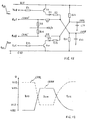
- the transistors T1 and T11 of the driver stage of the subscriber module are blocked for a recessive bit of the transmission signal and the voltage levels on the data lines CANH and CANL are due to the load resistors R21 and R22 and, if applicable, an adaptation impedance AN between the data lines as in FIG. 2 outlined.
- the bus line levels in the recessive state are kept approximately at the operating potentials VCC and GND, since the resistors R5, R6, R15 and R16 in the receiving branch are generally of high impedance compared to R21, R22.
- the resistors R21, R22 are preferably only present once in the BUS system, for example in the case of a system participant working as a master.
- the resistors R21, R22 are dimensioned taking into account the cable capacitances C23, C24 and the bit duration of the data transmission. Therefore, no appreciable current flows on the data lines during the recessive bit state.
- the dominant bit state Dom is produced by simultaneously switching on the transistors T1 and T11 of the driver stage by means of the transmission signal.
- a transmission current flows through T1, D2, R3 and R21 as well as through R22, R13, D12 and T11.
- the BUS line levels are determined by the voltage drop at T1, D2 or T11, D12 and the voltage dividers R3, R21 or R22, R13.
- the resistance values for R3, R13 are chosen to be significantly smaller than those for R21, R22, for example 30 ⁇ versus 240 ⁇ .
- the course of the resulting voltages on the data lines CANH, CANL is shown in FIG.
- ULR and ULD denote the voltage of the CANL line, UHR and UHD that of the CANH line in the recessive or dominant bit state in each case against GND.
- UHR is approximately zero and ULR is approximately equal to the operating voltage.
- diodes D2, D12 take into account the fact that several transmission driver stages can be active at the same time.
- the resistors R4, R14 serve as series resistors in the drive lines of the transistors T1, T11.
- the base connections of these transistors can also be connected in a known manner to the respective emitter connections via bleeder resistors.
- the resistors R5, R6 or R15, R16 form voltage dividers, which from the voltages of the BUS lines form the receive voltages CANH ', CANL' derive the inputs Rx1, Rxo of a comparator.
- the comparator interprets CANH '> CANL' as the dominant bit state, CANH ' ⁇ CANL' as the recessive bit state.
- the divider ratio of these voltage dividers is, for example, 10: 1 and ensures that the common-mode control range of the comparator is not exceeded even in the event of a DC voltage offset of the operating voltages.
- the receive trains are preferably symmetrical to a reference potential at VCC / 2. With regard to EMC problems, the entire circuit is largely symmetrical to the potential VCC / 2, i.e. all elements intended for CANH are also complementary for CANL. Further configurations of the basic circuit outlined and comparable circuits are familiar to the person skilled in the art.
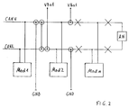
- FIG. 2 The subscribers connected to such a BUS system in a vehicle are generally distributed over the entire vehicle.
- FIG. 2 There are a number of possible faults to consider.
- FIG. 2 are the most important faults in the form of line interruptions (crosses) or short circuits (circled connection points) between the data lines with each other or against the potential VBat or GND of the vehicle electrical system.
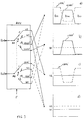
- FIG. 3 On the right are the four proposed operating modes a) to d) as a profile of the voltages present at the inputs RxO, Rx1 of the receiving comparator with a double bit change as in FIG. 1B outlined.
- the voltage applied to Rx1 is shown with a solid line, the voltage applied to RxO with a broken line.
- the receive voltages CANH ', CANL' also form the input voltages of the comparator.
- the constant voltage U1 is applied to the input RxO of the comparator as a replacement for the received voltage of the disturbed line CANL.
- the receive voltage CANH ' is at the other input and is assumed to be undisturbed.
- the receive voltage CANH 'at the comparator input Rx1 is replaced by a constant voltage U2, while the receive voltage CANL' is present at RxO.
- the voltages U1, U2 are advantageously in the middle of the level swings of CANH',. CANL '.
- the operating modes can be switched, for example, by means of a multiplexer arrangement MUX with two 4: 1 multiplexers M1 and MO, which are actuated synchronously by a control signal S from the controller and each forward one of the received voltages or one of the constant voltages to the respective comparator input as described.
- MUX multiplexer arrangement
- the particular advantage of the multiplexer arrangement can be seen in the free assignment of the constant voltages U1, U2 to RxO and Rx1, as a result of which U1 and U2 can be designed for maximum interference immunity against line interference.
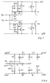
- FIG. 4 As means for separating the circuits are shown in FIG. 4 starting from the in FIG. 1A outlined basic circuit transistors T8, T18, T25 and T26 provided with series resistors R9, R19, R27 and R28.
- FIG. 1A corresponding elements are provided with reference numerals only to the extent necessary for explanation.
- transistors T25 and T26 are conductive, while T8 and T18 are blocking.
- the control signal S taking into account the transistor types in the sketched case, for example SI is on GND and SII is on VCC.
- the load circuits via R22 and R21 are thus closed and the operation of the transmission driver stages with transistors T1, T11 is unimpeded.
- single-wire mode b) according to FIG. 3 the received voltage derived from the CANL line is not evaluated and the CANL line is therefore not required for data transmission.
- this single-wire mode is taken into account in that the partial signal SI is switched to VCC.
- the sketched circuit enables low-loss operation even in the event of a malfunction, using the usual controller components.
- the controller can also be modified by emitting only one or no transmission signal at connections TxO, Tx1, depending on the operating mode.
- Bipolar planar transistors have transit frequencies> 100MHz in the linear range. In saturated switch mode, the large asymmetry ensures long delay times when changing from saturated to blocked mode. On the other hand, the two-wire transmission system is sensitive to overlap errors of CANH and CANL because this causes common-mode voltage impulses to reach the line, which interfere with the radio and other electronics. 5 a further development of the circuit according to FIG. 4 with funds for fast forced discharge for the driver transistors T1 and T11.
- interference voltages can possibly would be a multiple of the useful voltages and would be the input comparator in its common mode control range e.g. Overrun from +1 to + 4V against GND and lead to transmission errors.
- FIG. 6 shown in FIG. 1 indicated voltage divider 5, 6 and 15, 16 advantageously-wise designed as an RC filter (51 to 56, 61 to 66.
- a voltage divider 71 to 74 with low resistance to the filter resistors) is shown for VCC / 2 and U1 or U2.
- the two-part RC filter achieves considerable advantages over a simple RC filter with little additional effort. Without significantly worsening the pulse shape compared to a unified one, it has about twice the wide attenuation in dB at high frequencies. Because the common mode voltage is measured and acts against the reference potential GND, the filter halves must be reasonably the same so that the differential voltage CANH 'versus CANL' becomes small.
- the absolute size of the capacitor pairs 55, 65, 63, 53 is not critical.
- the resistors 51 and 61 are used on each driver to set the potential when the line is interrupted to the recessive state. They are much larger than R21 and R22. This filter is an essential contribution to the EMC resistance of a CAN transmission system.
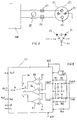
- FIG. 7 shown balancing choke 80 between driver stage 100 and cable 82 with signal lines 83, 84 and ground lines 85 only acts in the dominant state from a low-resistance source on the low-resistance cable as damping for common-mode signals and push-pull harmonics.
- the high-resistance input circuit in the recessive (receive state) does not allow any current to flow and the choke no longer forms a voltage divider because the input resistance of the receive train is significantly higher than the choke resistance.
- there is a damping bead 81 in between switched which transforms enough damping resistance to reliably prevent vibration.
- the cable replacement image in FIG. 7 is intended for cables with a star-shaped arrangement of the wires, which has almost the same qualities as a shielded cable in this circuitry, without having its disadvantages in terms of price and assembly.
- the power loss to be taken into account in the components involved is reduced to such an extent that extensive integration of the components shown in FIG. 4 to FIG. 6 outlined circuits is possible.
- several receive comparators for different operating modes as well as the multiplexer arrangement can be included without any significant additional effort.
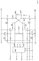
- Such an arrangement is shown in FIG. 8 outlined.
- the filters, the pnp transistor T25, the particularly loaded resistors R3, R13, R21 and R22 and the diodes D2, D12 are implemented as external circuitry of the integrated circuit IC.
- Only one of the complementary signals, for example TxO, is provided as the send signal from the controller module.
- the complementary transmit signal Tx1 can be generated internally in the IC module.
- the output signal of the multiplexer at Rx1 already represents a demodulated data signal.
- the input RxO of the controller is supplied with a constant reference voltage Ref, for example VCC / 2.
- the control of the multiplexer and the separation of circuits takes place simultaneously via the control signal S (SI, SII) as described.
- SI control signal
- the circuit is implemented in bipolar technology.
Landscapes
- Engineering & Computer Science (AREA)
- Computer Networks & Wireless Communication (AREA)
- Signal Processing (AREA)
- Power Engineering (AREA)
- Quality & Reliability (AREA)
- Dc Digital Transmission (AREA)
Applications Claiming Priority (2)
| Application Number | Priority Date | Filing Date | Title |
|---|---|---|---|
| DE4327035A DE4327035A1 (de) | 1993-08-12 | 1993-08-12 | Anordnung zur bidirektionalen Datenübertragung |
| DE4327035 | 1993-08-12 |
Publications (3)
| Publication Number | Publication Date |
|---|---|
| EP0643515A2 true EP0643515A2 (fr) | 1995-03-15 |
| EP0643515A3 EP0643515A3 (fr) | 1997-06-25 |
| EP0643515B1 EP0643515B1 (fr) | 2001-06-13 |
Family
ID=6494992
Family Applications (1)
| Application Number | Title | Priority Date | Filing Date |
|---|---|---|---|
| EP94112078A Expired - Lifetime EP0643515B1 (fr) | 1993-08-12 | 1994-08-03 | Dispositif pour la transmission bidirectionnelle de données |
Country Status (2)
| Country | Link |
|---|---|
| EP (1) | EP0643515B1 (fr) |
| DE (2) | DE4327035A1 (fr) |
Cited By (4)
| Publication number | Priority date | Publication date | Assignee | Title |
|---|---|---|---|---|
| EP0964556A3 (fr) * | 1998-06-12 | 2001-11-14 | STMicroelectronics GmbH | Circuit de traitement d'erreurs pour station réceptrice d'un système de transmission de données |
| CN100384232C (zh) * | 2005-08-02 | 2008-04-23 | 东杰电气(上海)有限公司 | 单线准双向通信方法 |
| WO2015014550A1 (fr) * | 2013-07-30 | 2015-02-05 | Robert Bosch Gmbh | Poste d'abonné pour un système de bus et procédé pour améliorer la robustesse aux erreurs d'un poste d'abonné d'un système de bus |
| US12047061B2 (en) | 2020-11-11 | 2024-07-23 | Aptiv Technologies AG | Bidirectional communication circuit, system and method for bidirectional communication |
Families Citing this family (4)
| Publication number | Priority date | Publication date | Assignee | Title |
|---|---|---|---|---|
| DE19611944C2 (de) | 1996-03-26 | 2003-03-27 | Daimler Chrysler Ag | Integrierter Schaltkreis zur Kopplung eines mikrokontrollierten Steuergerätes an einen Zweidraht-Bus |
| DE10133441C2 (de) * | 2001-07-10 | 2003-10-30 | Knorr Bremse Systeme | Schaltungsanordnung zur Spannungssymmetrierung von Datenbussen |
| DE10251473B3 (de) * | 2002-11-05 | 2004-06-17 | Siemens Ag | Schutzschaltung zum Schutz gegen Überspannung für einen CAN-Bus-Transceiver |
| DE102006038152B4 (de) * | 2006-08-16 | 2014-08-28 | Semikron Elektronik Gmbh & Co. Kg | Schaltung für Treiber und Systeme der Leistungselektronik |
Family Cites Families (8)
| Publication number | Priority date | Publication date | Assignee | Title |
|---|---|---|---|---|
| DE3021786A1 (de) * | 1980-06-10 | 1981-12-17 | Siemens AG, 1000 Berlin und 8000 München | Verfahren zur herstelung von elektrishen bauelementen, insbesondere schichtkondensatoren |
| US5050187A (en) * | 1988-04-12 | 1991-09-17 | The Furukawa Electric Co., Ltd. | Communication system equipped with an AC coupling receiver circuit |
| DE3901589A1 (de) * | 1989-01-20 | 1990-07-26 | Bosch Gmbh Robert | Ankopplung eines busteilnehmers |
| JP2768520B2 (ja) * | 1989-02-17 | 1998-06-25 | ローベルト ボツシユ ゲゼルシヤフト ミツト ベシユレンクテル ハフツング | ネツトワークインターフエース |
| DE3912335C2 (de) * | 1989-04-14 | 1997-07-24 | Siemens Ag | Verfahren und Anordnung zum Prüfen von mehradrigen Datenübertragungswegen |
| DE3937814A1 (de) * | 1989-11-14 | 1991-05-23 | Ant Nachrichtentech | Verfahren zur uebertragung von daten sowie anordnung |
| DE4005339A1 (de) * | 1990-02-20 | 1991-08-29 | Weidmueller C A Gmbh Co | Einrichtung zur digitalen informationsuebertragung |
| FR2680294B1 (fr) * | 1991-08-07 | 1993-11-19 | Peugeot | Dispositif de transmission d'informations en differentiel entre au moins deux organes d'un vehicule automobile. |
-
1993
- 1993-08-12 DE DE4327035A patent/DE4327035A1/de not_active Withdrawn
-
1994
- 1994-08-03 EP EP94112078A patent/EP0643515B1/fr not_active Expired - Lifetime
- 1994-08-03 DE DE59409781T patent/DE59409781D1/de not_active Expired - Lifetime
Cited By (6)
| Publication number | Priority date | Publication date | Assignee | Title |
|---|---|---|---|---|
| EP0964556A3 (fr) * | 1998-06-12 | 2001-11-14 | STMicroelectronics GmbH | Circuit de traitement d'erreurs pour station réceptrice d'un système de transmission de données |
| US6374374B1 (en) | 1998-06-12 | 2002-04-16 | Stmicroelectronics Gmbh | Error processing circuit for a receiving location of a data transmission system |
| CN100384232C (zh) * | 2005-08-02 | 2008-04-23 | 东杰电气(上海)有限公司 | 单线准双向通信方法 |
| WO2015014550A1 (fr) * | 2013-07-30 | 2015-02-05 | Robert Bosch Gmbh | Poste d'abonné pour un système de bus et procédé pour améliorer la robustesse aux erreurs d'un poste d'abonné d'un système de bus |
| US10268624B2 (en) | 2013-07-30 | 2019-04-23 | Robert Bosch Gmbh | Subscriber station for a bus system and method for improving the error tolerance of a subscriber station of a bus system |
| US12047061B2 (en) | 2020-11-11 | 2024-07-23 | Aptiv Technologies AG | Bidirectional communication circuit, system and method for bidirectional communication |
Also Published As
| Publication number | Publication date |
|---|---|
| EP0643515B1 (fr) | 2001-06-13 |
| DE59409781D1 (de) | 2001-07-19 |
| EP0643515A3 (fr) | 1997-06-25 |
| DE4327035A1 (de) | 1995-02-16 |
Similar Documents
| Publication | Publication Date | Title |
|---|---|---|
| DE10349600B4 (de) | Verfahren zur Überprüfung von Leitungsfehlern in einem Bussystem und Bussystem | |
| DE60005365T2 (de) | Elektrische isolierungsvorrichtung mit optokoppler für bidirektionelle anschlussleitungen | |
| EP2122924A2 (fr) | Circuiterie pour un bus de données de véhicule à moteur | |
| EP0500557B1 (fr) | Circuit multiplex, notamment pour commander des postes consommateurs dans des vehicules a moteur | |
| DE102015121732A1 (de) | Schaltungsanordnung für einen schaltbaren Leitungsabschluss eines seriellen Busses | |
| EP1568149B1 (fr) | Circuit de protection contre la surtension pour un emetteur-recepteur de bus can | |
| DE4307794C2 (de) | Einrichtung zur Überwachung symmetrischer Zweidraht-Busleitungen und -Busschnittstellen | |
| EP1194858B1 (fr) | Dispositif de transmission de donnees | |
| EP2428942B1 (fr) | Installation d'alerte aux dangers dotée de deux vitesses de transmission de données | |
| EP0643515B1 (fr) | Dispositif pour la transmission bidirectionnelle de données | |
| EP0234453B1 (fr) | Montage pour la transmission de données en série entre plusieurs terminaux | |
| DE3402633A1 (de) | Schaltungsanordnung zum anschalten eines teilnehmers an eine busleitung | |
| EP0977406B1 (fr) | Circuit de transmission de signaux numériques avec séparation galvanique | |
| WO1996034458A1 (fr) | Amplificateur de sortie gtl pour injecter un signal d'entree se trouvant a une entree dans une ligne de transmission situee a la sortie | |
| WO2015014552A1 (fr) | Agencement pour raccorder un composant à un module de commande maître d'un véhicule | |
| EP0427921A2 (fr) | Méthode et dispositif de transmission de données | |
| DE19647131C2 (de) | Vorrichtung und Verfahren zur zeitmultiplexen Übertragung von Informationen | |
| DE69132259T2 (de) | Vorrichtung zur spannungseinstellung in einem multiplexübertragungssystem | |
| WO1990008437A2 (fr) | Raccordement de postes a des bus | |
| EP0332055B1 (fr) | Circuit pour la détection de niveaux défectueux de signaux numériques qui sont injectés sur un bus | |
| EP0171555B1 (fr) | Système de ligne bus comportant deux conducteurs de signaux connectés à des dispositifs de transmission par deux sorties différentielles | |
| WO2023031017A1 (fr) | Système de transmission et procédé de transmission pour transmettre des données et de l'énergie par l'intermédiaire d'une ligne à deux fils | |
| DE19813952C1 (de) | Signalisierungsendstufe zur Erzeugung digitaler Spannungssignale auf einem Bussystem | |
| DE102017113538B4 (de) | Steuereinrichtung für einen Leistungshalbleiterschalter | |
| DE10133441C2 (de) | Schaltungsanordnung zur Spannungssymmetrierung von Datenbussen |
Legal Events
| Date | Code | Title | Description |
|---|---|---|---|
| PUAI | Public reference made under article 153(3) epc to a published international application that has entered the european phase |
Free format text: ORIGINAL CODE: 0009012 |
|
| AK | Designated contracting states |
Kind code of ref document: A2 Designated state(s): DE FR GB IT |
|
| PUAL | Search report despatched |
Free format text: ORIGINAL CODE: 0009013 |
|
| AK | Designated contracting states |
Kind code of ref document: A3 Designated state(s): DE FR GB IT |
|
| 17P | Request for examination filed |
Effective date: 19970915 |
|
| RAP1 | Party data changed (applicant data changed or rights of an application transferred) |
Owner name: DAIMLERCHRYSLER AG |
|
| 17Q | First examination report despatched |
Effective date: 19991116 |
|
| GRAG | Despatch of communication of intention to grant |
Free format text: ORIGINAL CODE: EPIDOS AGRA |
|
| GRAG | Despatch of communication of intention to grant |
Free format text: ORIGINAL CODE: EPIDOS AGRA |
|
| GRAH | Despatch of communication of intention to grant a patent |
Free format text: ORIGINAL CODE: EPIDOS IGRA |
|
| GRAH | Despatch of communication of intention to grant a patent |
Free format text: ORIGINAL CODE: EPIDOS IGRA |
|
| GRAA | (expected) grant |
Free format text: ORIGINAL CODE: 0009210 |
|
| AK | Designated contracting states |
Kind code of ref document: B1 Designated state(s): DE FR GB IT |
|
| PG25 | Lapsed in a contracting state [announced via postgrant information from national office to epo] |
Ref country code: IT Free format text: LAPSE BECAUSE OF FAILURE TO SUBMIT A TRANSLATION OF THE DESCRIPTION OR TO PAY THE FEE WITHIN THE PRE;WARNING: LAPSES OF ITALIAN PATENTS WITH EFFECTIVE DATE BEFORE 2007 MAY HAVE OCCURRED AT ANY TIME BEFORE 2007. THE CORRECT EFFECTIVE DATE MAY BE DIFFERENT FROM THE ONE RECORDED.SCRIBED TIME-LIMIT Effective date: 20010613 |
|
| REF | Corresponds to: |
Ref document number: 59409781 Country of ref document: DE Date of ref document: 20010719 |
|
| GBT | Gb: translation of ep patent filed (gb section 77(6)(a)/1977) |
Effective date: 20010817 |
|
| ET | Fr: translation filed | ||
| REG | Reference to a national code |
Ref country code: GB Ref legal event code: IF02 |
|
| PLBE | No opposition filed within time limit |
Free format text: ORIGINAL CODE: 0009261 |
|
| STAA | Information on the status of an ep patent application or granted ep patent |
Free format text: STATUS: NO OPPOSITION FILED WITHIN TIME LIMIT |
|
| 26N | No opposition filed | ||
| PGFP | Annual fee paid to national office [announced via postgrant information from national office to epo] |
Ref country code: GB Payment date: 20090827 Year of fee payment: 16 |
|
| REG | Reference to a national code |
Ref country code: FR Ref legal event code: CD Ref country code: FR Ref legal event code: CA |
|
| PGFP | Annual fee paid to national office [announced via postgrant information from national office to epo] |
Ref country code: DE Payment date: 20100823 Year of fee payment: 17 |
|
| GBPC | Gb: european patent ceased through non-payment of renewal fee |
Effective date: 20100803 |
|
| REG | Reference to a national code |
Ref country code: FR Ref legal event code: ST Effective date: 20110502 |
|
| PG25 | Lapsed in a contracting state [announced via postgrant information from national office to epo] |
Ref country code: FR Free format text: LAPSE BECAUSE OF NON-PAYMENT OF DUE FEES Effective date: 20100831 |
|
| PG25 | Lapsed in a contracting state [announced via postgrant information from national office to epo] |
Ref country code: GB Free format text: LAPSE BECAUSE OF NON-PAYMENT OF DUE FEES Effective date: 20100803 |
|
| PGFP | Annual fee paid to national office [announced via postgrant information from national office to epo] |
Ref country code: FR Payment date: 20090914 Year of fee payment: 16 |
|
| REG | Reference to a national code |
Ref country code: DE Ref legal event code: R119 Ref document number: 59409781 Country of ref document: DE Effective date: 20120301 |
|
| PG25 | Lapsed in a contracting state [announced via postgrant information from national office to epo] |
Ref country code: DE Free format text: LAPSE BECAUSE OF NON-PAYMENT OF DUE FEES Effective date: 20120301 |