EP0644678B1 - Empfänger für ASK-modulierte Mikrowellensignale - Google Patents
Empfänger für ASK-modulierte Mikrowellensignale Download PDFInfo
- Publication number
- EP0644678B1 EP0644678B1 EP94109388A EP94109388A EP0644678B1 EP 0644678 B1 EP0644678 B1 EP 0644678B1 EP 94109388 A EP94109388 A EP 94109388A EP 94109388 A EP94109388 A EP 94109388A EP 0644678 B1 EP0644678 B1 EP 0644678B1
- Authority
- EP
- European Patent Office
- Prior art keywords
- receiver
- ask
- antenna
- substrate
- varactor diode
- Prior art date
- Legal status (The legal status is an assumption and is not a legal conclusion. Google has not performed a legal analysis and makes no representation as to the accuracy of the status listed.)
- Expired - Lifetime
Links
- 239000000758 substrate Substances 0.000 claims description 10
- 230000008878 coupling Effects 0.000 claims 1
- 238000010168 coupling process Methods 0.000 claims 1
- 238000005859 coupling reaction Methods 0.000 claims 1
- 230000035945 sensitivity Effects 0.000 abstract description 4
- 238000009434 installation Methods 0.000 abstract 1
- 238000006243 chemical reaction Methods 0.000 description 4
- 238000010586 diagram Methods 0.000 description 3
- 230000036962 time dependent Effects 0.000 description 2
- 230000003247 decreasing effect Effects 0.000 description 1
- 238000001914 filtration Methods 0.000 description 1
- 230000010354 integration Effects 0.000 description 1
- 239000000463 material Substances 0.000 description 1
- 230000003595 spectral effect Effects 0.000 description 1
- 230000003068 static effect Effects 0.000 description 1
Images


Classifications
-
- H—ELECTRICITY
- H04—ELECTRIC COMMUNICATION TECHNIQUE
- H04L—TRANSMISSION OF DIGITAL INFORMATION, e.g. TELEGRAPHIC COMMUNICATION
- H04L27/00—Modulated-carrier systems
- H04L27/02—Amplitude-modulated carrier systems, e.g. using on-off keying; Single sideband or vestigial sideband modulation
- H04L27/06—Demodulator circuits; Receiver circuits
Definitions
- the present invention relates to a receiver for ASK-modulated Microwave signals, which is at least one has non-linear element envelope detector.
- the beacons send ASK (Amplitude Shift Keying) -modulated signals, which with one by very little circuitry awarding envelope detector received.
- an envelope detector consists essentially of at least one nonlinear element (e.g. Schottky diode), which represents a controlled resistance.
- the Predefined impedance of an integrated in the "On Board Unit" Antenna is on with the help of a suitable adapter circuit the controlled resistance of the envelope detector adapt.
- the use of a controlled active resistance to demodulate the ASK-modulated signals significant loss of conversion. This loss of conversion at the receiver input leads without low noise preamplification poor input sensitivity that beyond still by the low-frequency noise components of the controlled active resistance is further reduced.
- the detector consists of one Diode, which represents a controlled effective resistance.
- the Diode is an R / C element for integrating the detected Radar pulses downstream.
- the invention is based on the object To specify recipients of the type mentioned at the outset as little switching effort as possible a higher Input sensitivity is achieved than with a Envelope curve detector with controlled active resistance.
- Microwave signals has an antenna A, which is preferably in Stripline technology is realized, and one of them connected envelope detector, its nonlinear Element a controlled reactance VD, z. Legs Varactoriode is.
- the circuit described can also be used as a modulator operate. This can be done by pure Voltage control of the varactor diode VD takes place without power.
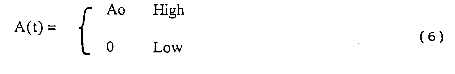
- a voltage U (t) the resonance circuit, formed from the varactor diode VD and the antenna A detuned and thereby a keying of the high-frequency signal enables.
- the parameters of the keying are determined by the Quality of service and the size of the applied voltage U (t) certainly.
- C (U) C 0 1+ 1- U ⁇
- ⁇ is the static operating point potential.
- U 0 is the DC voltage at the operating point
- L denotes an inductance.
- This DC component is about the operational quality of the district excessive present at the output of the circuit. So it's with to expect significantly cheaper conversion behavior.
- the noise present on the input side is in the treated the same way. The available noise power increases with decreasing bandwidth. Additional low frequency Noise components due to shot or sparkle noise are not available.
- the practical implementation of the circuit can be in multiple Way.
- the HF technical layout is oriented first on the type of antenna used.
- For applications in traffic control technology are exclusive Stripline circuits are provided. Lying in this case Cable and antenna on one side of the used Substrate material, a varactor diode can be used in a suitable Housing can be applied directly to the stripline.
- the NF connection or the supply of a control voltage for the Modulation can then e.g. via a high-resistance line respectively.
- FIG. 3 shows one Arrangement in the upper part in a top view and in the lower Part in a cross section B-B.
- a planar antenna element A and its associated ground line M inside the substrate S.
- the lead LE On the The underside of the substrate S is the lead LE to the antenna A and possibly other circuit elements applied.
- the antenna A is connected to the lead LE via a Vias in the substrate S.
- the vias from planar antenna element A to line LE happens advantageously via the housing in a hole in the Substrate S used varactor diode VD.
- a diversity receiver can be seen in FIG. Here are two antennas A1 and A2, each with a varactor diode VD1, VD2 connected.
- the detected low-frequency Output signals are combined by an adder AD.
- AD adder
Landscapes
- Engineering & Computer Science (AREA)
- Computer Networks & Wireless Communication (AREA)
- Signal Processing (AREA)
- Input Circuits Of Receivers And Coupling Of Receivers And Audio Equipment (AREA)
- Digital Transmission Methods That Use Modulated Carrier Waves (AREA)
- Traffic Control Systems (AREA)
- Circuits Of Receivers In General (AREA)
Description
Claims (5)
- Empfänger für ASK-modulierte Mikrowellensignale, welcher einen mindestens ein nichtlineares Element aufweisenden Hüllkurvendetektor besitzt, dadurch gekennzeichnet, daß das nichtlineare Element (VD, VD1, VD2) überwiegend aus einem gesteuerten Blindwiderstand besteht.
- Empfänger nach Anspruch 1, dadurch gekennzeichnet, daß das nichtlineare Element (VD, VD1, VD2) eine Varaktoriode ist.
- Empfänger nach Anspruch 1, dadurch gekennzeichnet, daß das nichtlineare Element (VD, VD1, VD2) zusammen mit einer daran angeschlossenen planaren Antenne (A, A1, A2) einen Resonanzkreis bildet.
- Empfänger nach einem der vorhergehenden Ansprüche, dadurch gekennzeichnet, daß zwei jeweils mit einer eigenen Antenne (A1, A2) gekoppelte nichtlineare Elemente (VD1, VD2) im Gegentakt geschaltet sind und daß ein Addierer (AD) die an den nichtlinearen Elementen (VD1, VD2) detektierten Signale zusammenfaßt.
- Empfänger nach einem der vorhergehenden Ansprüche, dadurch gekennzeichnet, daß die Kopplung einer planaren Antenne (A) auf einer Seite eines Substrats (S) mit einer planaren Zuleitung (LE) auf der gegenüberliegenden Seite des Substrats (S) über eine mit der Antenne (A) verbundene und durch das Substrat (S) geführte Varaktordiode (VD) erfolgt.
Applications Claiming Priority (2)
| Application Number | Priority Date | Filing Date | Title |
|---|---|---|---|
| DE4329122 | 1993-08-30 | ||
| DE4329122A DE4329122C1 (de) | 1993-08-30 | 1993-08-30 | Empfänger für ASK-modulierte Mikrowellensignale |
Publications (2)
| Publication Number | Publication Date |
|---|---|
| EP0644678A1 EP0644678A1 (de) | 1995-03-22 |
| EP0644678B1 true EP0644678B1 (de) | 2000-03-15 |
Family
ID=6496336
Family Applications (1)
| Application Number | Title | Priority Date | Filing Date |
|---|---|---|---|
| EP94109388A Expired - Lifetime EP0644678B1 (de) | 1993-08-30 | 1994-06-17 | Empfänger für ASK-modulierte Mikrowellensignale |
Country Status (3)
| Country | Link |
|---|---|
| EP (1) | EP0644678B1 (de) |
| AT (1) | ATE190789T1 (de) |
| DE (2) | DE4329122C1 (de) |
Families Citing this family (2)
| Publication number | Priority date | Publication date | Assignee | Title |
|---|---|---|---|---|
| DE19650093C1 (de) * | 1996-12-03 | 1997-10-23 | Fraunhofer Ges Forschung | Empfänger mit niedrigem Ruhestrom |
| DE19858099C2 (de) * | 1998-12-16 | 2000-12-07 | Texas Instruments Deutschland | Demodulatorschaltung |
Family Cites Families (4)
| Publication number | Priority date | Publication date | Assignee | Title |
|---|---|---|---|---|
| US4075571A (en) * | 1977-06-08 | 1978-02-21 | General Dynamics Corporation | Externally biased video detector circuit for limiting clutter and noise in a detected radar signal |
| US4249134A (en) * | 1978-12-27 | 1981-02-03 | Aei Semiconductors Limited | Radio frequency detectors |
| DE4035398A1 (de) * | 1990-11-07 | 1992-05-14 | Bosch Gmbh Robert | Verfahren zur hochfrequenten datenuebertragung von fahrinformationen und vorrichtung dazu |
| ES2087919T3 (es) * | 1991-02-05 | 1996-08-01 | Siemens Ag | Circuito desmodulador integrable. |
-
1993
- 1993-08-30 DE DE4329122A patent/DE4329122C1/de not_active Expired - Fee Related
-
1994
- 1994-06-17 DE DE59409201T patent/DE59409201D1/de not_active Expired - Fee Related
- 1994-06-17 AT AT94109388T patent/ATE190789T1/de active
- 1994-06-17 EP EP94109388A patent/EP0644678B1/de not_active Expired - Lifetime
Also Published As
| Publication number | Publication date |
|---|---|
| DE59409201D1 (de) | 2000-04-20 |
| DE4329122C1 (de) | 1995-03-02 |
| ATE190789T1 (de) | 2000-04-15 |
| EP0644678A1 (de) | 1995-03-22 |
Similar Documents
| Publication | Publication Date | Title |
|---|---|---|
| DE60024225T2 (de) | Funksender | |
| DE19627640C2 (de) | Mischer | |
| EP1406349B1 (de) | Aktive Breitband-Empfangsantenne mit Empfangspegel-Regelung | |
| EP1246294B1 (de) | Aktive Breitband-Fahrzeugempfangsantenne | |
| DE4017625A1 (de) | Mikrowellen-antwortsender | |
| DE68923245T2 (de) | Phasendetektor für eine Niederfrequenz-Wellenform enthaltende in Amplitude modulierte Hochfrequenzsignale. | |
| DE19955849B4 (de) | Phasenschieber | |
| EP0644678B1 (de) | Empfänger für ASK-modulierte Mikrowellensignale | |
| EP0089078B1 (de) | Schaltungsanordnung für einen FM-Empfänger | |
| DE3108980A1 (de) | Doppler-drehfunkfeuer | |
| DE102005037877A1 (de) | Diodenmischer | |
| DE2833056A1 (de) | Hf-verstaerker | |
| WO1995026511A1 (de) | Fahrzeuggerät für transponderbetrieb | |
| DE10015315B4 (de) | Antennenverstärker und regelbares Stellglied | |
| DE69716146T2 (de) | Hochfrequenz-Leistungsmesseinrichtung | |
| DE2642434C3 (de) | Mikrowellenübertragungssystem | |
| DE2855552A1 (de) | Rauscharme antennenanordnung fuer einen automatischen radiokompass | |
| DE4307014A1 (en) | Car radio with FM and AM bands - uses two relatively short antenna elements with summation of their output signals in AM circuit | |
| DE19501113C1 (de) | Leitungsentzerrer | |
| DE3506817A1 (de) | Elektronische sende-empfangsumschaltvorrichtung fuer funkgeraete | |
| EP1859510A1 (de) | Aktives empfangsantennensystem | |
| DE2646035A1 (de) | Verstaerkerschaltung fuer wechselspannung | |
| DE102005025677B9 (de) | Empfangsverstärker, insbesondere für Fernsehempfänger und Verwendung des Empfangsverstärkers | |
| DE102021120119A1 (de) | Elektrische Schaltung zur Lastgeradenmodulation von linearen Leistungsverstärkern | |
| EP0520308A2 (de) | Verstärkende Schaltungsanordnung |
Legal Events
| Date | Code | Title | Description |
|---|---|---|---|
| PUAI | Public reference made under article 153(3) epc to a published international application that has entered the european phase |
Free format text: ORIGINAL CODE: 0009012 |
|
| 17P | Request for examination filed |
Effective date: 19941125 |
|
| AK | Designated contracting states |
Kind code of ref document: A1 Designated state(s): AT BE DE FR GB NL |
|
| RAP1 | Party data changed (applicant data changed or rights of an application transferred) |
Owner name: ROBERT BOSCH GMBH |
|
| 17Q | First examination report despatched |
Effective date: 19980316 |
|
| GRAG | Despatch of communication of intention to grant |
Free format text: ORIGINAL CODE: EPIDOS AGRA |
|
| GRAG | Despatch of communication of intention to grant |
Free format text: ORIGINAL CODE: EPIDOS AGRA |
|
| GRAH | Despatch of communication of intention to grant a patent |
Free format text: ORIGINAL CODE: EPIDOS IGRA |
|
| GRAH | Despatch of communication of intention to grant a patent |
Free format text: ORIGINAL CODE: EPIDOS IGRA |
|
| GRAA | (expected) grant |
Free format text: ORIGINAL CODE: 0009210 |
|
| AK | Designated contracting states |
Kind code of ref document: B1 Designated state(s): AT BE DE FR GB NL |
|
| REF | Corresponds to: |
Ref document number: 190789 Country of ref document: AT Date of ref document: 20000415 Kind code of ref document: T |
|
| REF | Corresponds to: |
Ref document number: 59409201 Country of ref document: DE Date of ref document: 20000420 |
|
| GBT | Gb: translation of ep patent filed (gb section 77(6)(a)/1977) |
Effective date: 20000612 |
|
| PGFP | Annual fee paid to national office [announced via postgrant information from national office to epo] |
Ref country code: AT Payment date: 20000712 Year of fee payment: 7 |
|
| ET | Fr: translation filed | ||
| PLBE | No opposition filed within time limit |
Free format text: ORIGINAL CODE: 0009261 |
|
| STAA | Information on the status of an ep patent application or granted ep patent |
Free format text: STATUS: NO OPPOSITION FILED WITHIN TIME LIMIT |
|
| 26N | No opposition filed | ||
| PG25 | Lapsed in a contracting state [announced via postgrant information from national office to epo] |
Ref country code: AT Free format text: LAPSE BECAUSE OF NON-PAYMENT OF DUE FEES Effective date: 20010617 |
|
| REG | Reference to a national code |
Ref country code: GB Ref legal event code: IF02 |
|
| PGFP | Annual fee paid to national office [announced via postgrant information from national office to epo] |
Ref country code: GB Payment date: 20020516 Year of fee payment: 9 |
|
| PGFP | Annual fee paid to national office [announced via postgrant information from national office to epo] |
Ref country code: FR Payment date: 20020610 Year of fee payment: 9 |
|
| PGFP | Annual fee paid to national office [announced via postgrant information from national office to epo] |
Ref country code: DE Payment date: 20020626 Year of fee payment: 9 |
|
| PGFP | Annual fee paid to national office [announced via postgrant information from national office to epo] |
Ref country code: NL Payment date: 20020628 Year of fee payment: 9 |
|
| PGFP | Annual fee paid to national office [announced via postgrant information from national office to epo] |
Ref country code: BE Payment date: 20020829 Year of fee payment: 9 |
|
| PG25 | Lapsed in a contracting state [announced via postgrant information from national office to epo] |
Ref country code: GB Free format text: LAPSE BECAUSE OF NON-PAYMENT OF DUE FEES Effective date: 20030617 |
|
| PG25 | Lapsed in a contracting state [announced via postgrant information from national office to epo] |
Ref country code: BE Free format text: LAPSE BECAUSE OF NON-PAYMENT OF DUE FEES Effective date: 20030630 |
|
| BERE | Be: lapsed |
Owner name: ROBERT *BOSCH G.M.B.H. Effective date: 20030630 |
|
| PG25 | Lapsed in a contracting state [announced via postgrant information from national office to epo] |
Ref country code: NL Free format text: LAPSE BECAUSE OF NON-PAYMENT OF DUE FEES Effective date: 20040101 Ref country code: DE Free format text: LAPSE BECAUSE OF NON-PAYMENT OF DUE FEES Effective date: 20040101 |
|
| GBPC | Gb: european patent ceased through non-payment of renewal fee |
Effective date: 20030617 |
|
| NLV4 | Nl: lapsed or anulled due to non-payment of the annual fee |
Effective date: 20040101 |
|
| PG25 | Lapsed in a contracting state [announced via postgrant information from national office to epo] |
Ref country code: FR Free format text: LAPSE BECAUSE OF NON-PAYMENT OF DUE FEES Effective date: 20050228 |
|
| REG | Reference to a national code |
Ref country code: FR Ref legal event code: ST |
|
| PG25 | Lapsed in a contracting state [announced via postgrant information from national office to epo] |
Ref country code: FR Free format text: LAPSE BECAUSE OF NON-PAYMENT OF DUE FEES Effective date: 20030630 |