EP0644700A2 - Système convertisseur de la fréquence d'échantillonnage - Google Patents
Système convertisseur de la fréquence d'échantillonnage Download PDFInfo
- Publication number
- EP0644700A2 EP0644700A2 EP94306625A EP94306625A EP0644700A2 EP 0644700 A2 EP0644700 A2 EP 0644700A2 EP 94306625 A EP94306625 A EP 94306625A EP 94306625 A EP94306625 A EP 94306625A EP 0644700 A2 EP0644700 A2 EP 0644700A2
- Authority
- EP
- European Patent Office
- Prior art keywords
- sampling rate
- converting
- video signal
- signal
- sampling
- Prior art date
- Legal status (The legal status is an assumption and is not a legal conclusion. Google has not performed a legal analysis and makes no representation as to the accuracy of the status listed.)
- Ceased
Links
Images




Classifications
-
- H—ELECTRICITY
- H04—ELECTRIC COMMUNICATION TECHNIQUE
- H04N—PICTORIAL COMMUNICATION, e.g. TELEVISION
- H04N7/00—Television systems
- H04N7/01—Conversion of standards, e.g. involving analogue television standards or digital television standards processed at pixel level
-
- H—ELECTRICITY
- H04—ELECTRIC COMMUNICATION TECHNIQUE
- H04N—PICTORIAL COMMUNICATION, e.g. TELEVISION
- H04N11/00—Colour television systems
- H04N11/04—Colour television systems using pulse code modulation
-
- H—ELECTRICITY
- H04—ELECTRIC COMMUNICATION TECHNIQUE
- H04N—PICTORIAL COMMUNICATION, e.g. TELEVISION
- H04N5/00—Details of television systems
- H04N5/44—Receiver circuitry for the reception of television signals according to analogue transmission standards
- H04N5/445—Receiver circuitry for the reception of television signals according to analogue transmission standards for displaying additional information
- H04N5/45—Picture in picture, e.g. displaying simultaneously another television channel in a region of the screen
-
- H—ELECTRICITY
- H04—ELECTRIC COMMUNICATION TECHNIQUE
- H04N—PICTORIAL COMMUNICATION, e.g. TELEVISION
- H04N9/00—Details of colour television systems
- H04N9/64—Circuits for processing colour signals
Definitions
- the present invention relates to a sampling rate converting system for converting a sampling rate of a video signal.
- a sampling frequency suitable for the TV system of the video signal should be used.
- the D2-MAC system usually uses a sampling frequency of 13.5 MHz.
- Such a video signal processing system converts a digital video signal into an analog video signal and then processes the analog video signal.
- the system converts a digital video signal into an analog video signal and then process the analog signal with a common sampling clock changed from the original sampling clock.
- an object of the present invention is to provide a sampling rate converting system that can convert different sampling frequencies of signals of a plurality of circuits into a common sampling frequency without an increase of circuit scale.
- Another object of the present invention is to provide a sampling rate converting system that can be easily extended.
- the present invention is a sampling rate converting system, comprising a plurality of circuit blocks for outputting digital signals with different sampling frequencies, a data bus for commonly connecting output ends of the circuit blocks, and a sampling rate converter having an input end connected to the data bus and being adapted for converting a sampling frequency of a digital signal received through the data bus into a predetermined sampling frequency, wherein the system is adapted for selecting one of outputs of the circuit blocks, sending the selected output to the sampling rate converter through the data bus, and converting a sampling frequency of the selected output into the predetermined sampling frequency.
- Each of the circuit blocks is connected to common buses (that are luminance signal bus and chroma signal bus).
- a common clock line for transmitting a clock is provided.
- the sampling rate converter can easily convert the output data of each circuit block to the common sampling rate with the clock being received.
- the sampling rate converter can deal with the outputs of a plurality of circuit blocks by itself.
- Each of the circuit blocks has a tri-state buffer at its output stage. In such a construction, with only an output enable signal that is supplied to a desired circuit block, this circuit block can be selected.
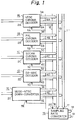
- Fig. 1 shows an embodiment of the present invention.
- the embodiment of the present invention is adapted for transmitting a plurality of digital video signals with different sampling frequencies on common buses. With such common buses, the outputs of circuit blocks with different sampling frequencies can be easily converted into a common sampling frequency.
- reference numerals 1A to 1E are circuit blocks that operate with different sampling frequencies.
- the circuit block 1A is an NTSC chroma decoder.
- the circuit block 1B is a PAL chroma decoder.
- the circuit block 1C is a SECAM chroma decoder.
- the circuit block 1D is a D2-MAC decoder.
- the circuit block 1E is a MUSE-NTSC decoder.
- the circuit blocks 1A to 1E have composite digital video signal input terminals 2A to 2E, digital luminance signal output terminals 3A to 3E, and digital chroma signal output terminal 4A to 4E, respectively.
- the digital chroma signal output terminals 4A to 4E multiplex digital color difference signals R-Y and B-Y corresponding to the time division multiplexing technique. In other words, since the frequency band of the color difference signals R-Y and B-Y is the half the frequency band of the luminance signal, the color difference signals R-Y and B-Y are transmitted one after the other.
- output enable signal input terminals 5A to 5E and clock output terminals 6A to 6E are provided. As shown in Fig.
- the circuit blocks 1A to 1E have tri-state buffers 7, 7, 7, ... at their output stages.
- An output enable signal is supplied from the output enable signal input terminals 5A to 5E.
- the output enable signal controls the tri-state buffers 7, 7, 7, ...
- the tri-state buffers 7, 7, 7, ... become active and high-impedance state when for example the output enable signal is "L" and "H", respectively.
- reference numerals 10 is a luminance signal bus.
- Reference numeral 11 is a chroma signal bus.
- the luminance signal output terminals 3A to 3E of the circuit blocks 1A to 1E are connected to the luminance signal bus 10 in common.
- the output terminals 4A to 4E of the circuit blocks 1A to 1E are connected to the chroma signal bus 11 in common.
- the corresponding bits of the luminance signal output terminals 3A to 3E of the circuit blocks 1A to 1E are connected to each other through the luminance signal bus 10 in such a manner that the MSB and LSB of one output terminal are connected to those of the other output terminals.
- the corresponding bits of the chroma signal output terminals 4A to 4E of the circuit blocks 1A to 1E are connected to each other through the chroma signal bus 11.
- the clock output terminals 6A to 6E of the circuit blocks 1A to 1E are connected to a clock line 12 in common.
- reference numeral 15 is a circuit block of a sampling rate converter.
- the sampling rate converter 15 has a digital luminance signal input terminal 16, a digital chroma signal input terminal 17, a digital luminance signal output terminal 18, a digital chroma signal output terminal 19, a clock input terminal 20, and a changing clock input terminal 21.
- the luminance signal input terminal 16 of the sampling rate converter circuit block 15 is connected to the luminance signal bus 10.
- the chroma signal input terminal 17 of the sampling rate converter circuit block 15 is connected to the chroma signal bus 11.
- the clock input terminal 20 of the sampling rate converter circuit block 15 is connected to the clock line 12.
- the sampling rate converter circuit block 15 converts sampling frequencies of digital luminance signals and digital chroma signals supplied through the luminance signal bus 10 and the chroma signal bus 11 into a sampling frequency (of for example 18 MHz that is 1144 f H in the NTSC system and 1152 f H in the PAL system) that is in common with all the system.
- a sampling frequency of for example 18 MHz that is 1144 f H in the NTSC system and 1152 f H in the PAL system
- the sampling rate converter circuit block 15 may be constructed as shown in Fig. 4 such as described in Japanese Patent Publication No. 127790/1992.
- reference numeral 51 is a digital signal input terminal.
- Reference numeral 52 is an input terminal of a sampling clock f s1 that has not been converted.
- Reference numeral 53 is an input terminal of a sampling clock f s2 that has been converted.
- the input terminal 51 corresponds to the luminance signal input terminal 16 or the chroma signal input terminal 17 of the sampling rate converter circuit block 15.
- the clock input terminal 52 corresponds to the clock input terminal 20 of the sampling rate converter circuit block 15.
- a digital signal with a sampling clock of f s1 is supplied from an input terminal 51.
- the digital signal is sent to registers 54-1, 54-2, ..., 54-n that are connected in series. Outputs between each stage of the registers 54-1 to 54-n have a sampling clock of f s2 and are sent to registers 55-1 to 55-n, respectively.
- the outputs of the registers 55-1 to 55-n are sent to multiplying circuits 56-1, 56-2, ..., 56-n, respectively.
- the clocks f s1 which is supplied from the input terminal 52, and the clock f s2 , which is supplied from the input terminal 53, are sent to a phase difference detecting circuit 57.
- the phase difference detecting circuit 57 detects the phase difference between the pre-converted clock f s1 and the post-converted clock f s2 .
- the output of the phase difference detecting circuit 57 is sent to a coefficient table 58.
- the coefficient table 58 generates a coefficient corresponding to the output of the phase difference detecting circuit 57.
- the coefficient of the coefficient table is sent to the multiplying circuits 56-1 to 56-n.
- the multiplying circuits 56-1 to 56-n multiply the outputs of the registers 55-1 to 55-n by the coefficient, respectively.
- the outputs of the multiplying circuits 56-1 to 56-n are sent to an adding circuit 59.
- the output of the adding circuit 59 is extracted from an output terminal 60.
- the output terminal 60 corresponds to the luminance signal output terminal 18 or the chroma signal output terminal 19 of the sampling rate converter circuit block 15.
- the sampling frequency f s1 of the digital signal supplied from the input terminal 51 is changed to the sampling frequency f s2 by the registers 55-1 to 55-n.
- the multiplying circuits 56-1 to 56-n and the adding circuit 59 performs filtering process.
- the output enable signal is sent to only the desired circuit block.
- the circuit block that has received the output enable signal outputs a luminance signal and a chroma signal. These luminance signal and the chroma signal are sent to the luminance signal bus 10 and the chroma signal bus 11, respectively.
- the luminance signal and the chroma signal are sent to the sampling rate converter circuit block 15.
- the sampling clock of the circuit block that has received the output enable signal is sent to the sampling rate converter circuit block 15 through the clock line 12.
- the sampling rate converter circuit block 15 converts the received sampling rate into a sampling rate that is common in all the systems.
- the luminance signal and the chroma signal are extracted from output terminals 18 and 19, respectively.
- an enable signal EN is sent to only the output enable signal input terminal 5B of the PAL chroma decoder circuit block 1B.
- the PAL chroma decoder circuit block 1B outputs a luminance signal Y-PAL and a chroma signal C-PAL that have been decoded. These signals are sent to the sampling rate converter circuit block 15 through the luminance signal bus 10 and the chroma signal bus 11, respectively.
- a sampling clock CK-PAL (of for example 17.734475 MHz) is sent from the PAL chroma decoder circuit block 1B to the sampling rate converter circuit block 15 through the clock line 12.
- the sampling rate converter circuit block 15 converts the sampling frequency of the PAL system into a sampling frequency that is common in all the system (for example, 18 MHz).
- an enable signal EN is supplied to only the enable signal input terminal 5A of the NTSC chroma decoder 1A.
- the NTSC chroma decoder circuit block 1A outputs a luminance signal Y-NTSC and a chroma signal C-NTSC that have been decoded. These signals are sent to the sampling rate converter circuit block 15 through the luminance signal bus 10 and the chroma signal bus 11, respectively.
- a sampling clock CK-NTSC (of for example 14.31818 MHz) is sent from the NTSC chroma decoder circuit block 1A to the sampling rate converter circuit block 15 through the clock line 12.
- the sampling rate converter circuit block 15 converts the sampling frequency of the NTSC system into a sampling frequency that is common in all the systems (for example, 18 MHz).
- the luminance signal and the chroma signal are extracted from the output terminals 18 and 19, respectively.
- the output of the circuit block of the desired system is sent to the sampling rate converter circuit block 15.
- the sampling rate converter circuit block 15 outputs the digital signal with the sampling frequency that is common in all the systems.
- the luminance signal bus 10 and the chroma signal bus 11, which transmit the luminance signal and the chroma signal, respectively are provided, circuit blocks can be easily added or deleted corresponding to new systems, thereby providing high extensibility.
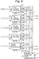
- Fig. 7 shows an example of PinP(picture in picture) signal processing circuit using such a sampling rate converter.
- a circuit block 31A is a video signal processing circuit for outputting a parent screen corresponding to a sampling rate converter 15 in Fig. 1. Digital luminance signal, digital chroma signal and clock are input to a circuit block 31A as input signals.
- a circuit block 31 is a PinP signal processing circuit for outputting a child screen.
- a circuit block 31B is composed with a sampling rate converter in Fig. 1 and interpolating and compensating circuit for generating child screen video signal.
- a circuit block 31C is a mixing signal processsing circuit for processing signal process to mixed a parents screen video signal and a child screen video signal, such as flicker, sharpness and aspect convertion process.
- Luminance signal output terminals 32A and 32B of the circuit blocks 31A and 31B are connected to a lminance signal bus 40 in common. Chroma signal output terminals 33A and 33B of the circuit blocks 31A and 31B are connected to a chroma signal bus 41 in common. Clock input terminals 34A and 34B of the circuit blocks 31A and 31B are connected to a clock bus 42 in common. Common clock CK to be changed is supplied to circuit block 31A and 31B through the clock line 42. An output enable signal EN is sent from the circuit block 31B to the circuit block 31A.
- Video signals of parents screen, which is input to a circuit block 31A, and video signals of child screen, which is input to a circuit block 31B, are changed to the common frequency CK.
- the resultant signals are sent to the luminanceu signal bus 40 and chroma signal bus 41, respectively.
- the output enable signal EN is supplied from the circuit block 31B to circuit block 31A.
- the output enable signal EN is not supplied.
- the video signal supplied from the circuit block 31A is sent to the circuit block 31C through the luminance signal bus 40 and chroma signal bus 41.
- the video signal supplied from the circuit block 31B is sent to a circuit block 31C through the luminance signal bus 40 and chroma signal bus 41.
- signal process after the sampling rate changing can be treated with one clock CK.
- parents screen signal is NTSC and parents screen signal is PAL, same process as above mentioned would be available.
- PinP signal processing circuit 31B is composed with two step circuits, which are the sampling rate converter circuit and the compensating and interpolating circuit for processing small picture in Fig. 1, whereas compensating and interpolating process would be done using the changing clock directly.
Landscapes
- Engineering & Computer Science (AREA)
- Multimedia (AREA)
- Signal Processing (AREA)
- Color Television Systems (AREA)
- Transmission Systems Not Characterized By The Medium Used For Transmission (AREA)
Applications Claiming Priority (2)
| Application Number | Priority Date | Filing Date | Title |
|---|---|---|---|
| JP5253808A JPH0787526A (ja) | 1993-09-16 | 1993-09-16 | サンプリングレート変換システム |
| JP253808/93 | 1993-09-16 |
Publications (2)
| Publication Number | Publication Date |
|---|---|
| EP0644700A2 true EP0644700A2 (fr) | 1995-03-22 |
| EP0644700A3 EP0644700A3 (fr) | 1996-05-29 |
Family
ID=17256438
Family Applications (1)
| Application Number | Title | Priority Date | Filing Date |
|---|---|---|---|
| EP94306625A Ceased EP0644700A3 (fr) | 1993-09-16 | 1994-09-09 | Système convertisseur de la fréquence d'échantillonnage. |
Country Status (4)
| Country | Link |
|---|---|
| US (1) | US5475436A (fr) |
| EP (1) | EP0644700A3 (fr) |
| JP (1) | JPH0787526A (fr) |
| KR (1) | KR950010618A (fr) |
Cited By (3)
| Publication number | Priority date | Publication date | Assignee | Title |
|---|---|---|---|---|
| WO1999052113A3 (fr) * | 1998-04-03 | 2000-01-06 | Avid Technology Inc | Previsualisation d'effets et d'edition tvhd utilisant des dispositifs tv standards |
| US6229576B1 (en) | 1998-04-03 | 2001-05-08 | Avid Technology, Inc. | Editing system with router for connection to HDTV circuitry |
| EP1271964A3 (fr) * | 2001-06-28 | 2003-04-23 | Sony Corporation | Appareil de traitement de signaux video |
Families Citing this family (4)
| Publication number | Priority date | Publication date | Assignee | Title |
|---|---|---|---|---|
| JP3395182B2 (ja) * | 1993-03-23 | 2003-04-07 | ソニー株式会社 | レートコンバータ及び撮像装置 |
| KR100305874B1 (ko) * | 1995-06-02 | 2001-11-30 | 모리시타 요이찌 | 다방식 텔레비전수상기 |
| US5712687A (en) * | 1996-04-25 | 1998-01-27 | Tektronix, Inc. | Chrominance resampling for color images |
| US6124880A (en) * | 1996-05-24 | 2000-09-26 | Nynex Science & Technology Inc. | Multi-user video switchable translator |
Family Cites Families (10)
| Publication number | Priority date | Publication date | Assignee | Title |
|---|---|---|---|---|
| JPS5916469A (ja) * | 1982-07-19 | 1984-01-27 | Matsushita Electric Ind Co Ltd | デジタル信号切替回路 |
| JPS6467019A (en) * | 1987-09-07 | 1989-03-13 | Yokogawa Electric Corp | Digital signal processor |
| US5057911A (en) * | 1989-10-19 | 1991-10-15 | Matsushita Electric Industrial Co., Ltd. | System and method for conversion of digital video signals |
| US5111160A (en) * | 1991-04-30 | 1992-05-05 | The Grass Valley Group | Clock generation circuit for multistandard serial digital video with automatic format identification |
| US5200749A (en) * | 1991-05-28 | 1993-04-06 | Tektronix, Inc. | Format converter architecture |
| JP3104085B2 (ja) * | 1991-10-18 | 2000-10-30 | ソニー株式会社 | 記録再生装置用送出システム |
| KR930015760A (ko) * | 1991-12-31 | 1993-07-24 | 강진구 | 텔레비젼모드 자동변환장치 |
| KR950003024B1 (ko) * | 1992-02-29 | 1995-03-29 | 삼성전자 주식회사 | 동기신호 발생장치 |
| US5347318A (en) * | 1992-06-16 | 1994-09-13 | Canon Kabushiki Kaisha | Apparatus for processing video signals having different aspect ratios |
| US5325131A (en) * | 1993-05-03 | 1994-06-28 | Tektronix, Inc. | Multiformat television switcher |
-
1993
- 1993-09-16 JP JP5253808A patent/JPH0787526A/ja active Pending
-
1994
- 1994-09-09 US US08/302,033 patent/US5475436A/en not_active Expired - Fee Related
- 1994-09-09 EP EP94306625A patent/EP0644700A3/fr not_active Ceased
- 1994-09-15 KR KR1019940023365A patent/KR950010618A/ko not_active Withdrawn
Cited By (5)
| Publication number | Priority date | Publication date | Assignee | Title |
|---|---|---|---|---|
| WO1999052113A3 (fr) * | 1998-04-03 | 2000-01-06 | Avid Technology Inc | Previsualisation d'effets et d'edition tvhd utilisant des dispositifs tv standards |
| US6226038B1 (en) | 1998-04-03 | 2001-05-01 | Avid Technology, Inc. | HDTV editing and effects previsualization using SDTV devices |
| US6229576B1 (en) | 1998-04-03 | 2001-05-08 | Avid Technology, Inc. | Editing system with router for connection to HDTV circuitry |
| EP1271964A3 (fr) * | 2001-06-28 | 2003-04-23 | Sony Corporation | Appareil de traitement de signaux video |
| US6947096B2 (en) | 2001-06-28 | 2005-09-20 | Sony Corporation | Video processing apparatus for converting composite video signals to digital component video signals |
Also Published As
| Publication number | Publication date |
|---|---|
| JPH0787526A (ja) | 1995-03-31 |
| EP0644700A3 (fr) | 1996-05-29 |
| US5475436A (en) | 1995-12-12 |
| KR950010618A (ko) | 1995-04-28 |
Similar Documents
| Publication | Publication Date | Title |
|---|---|---|
| US5475436A (en) | Sampling rate converting system for converting the sampling rate of a video signal | |
| US5138455A (en) | Video signal processing circuit for compressed picture insertion function of television receiver | |
| JP2556368B2 (ja) | ビデオ信号処理装置 | |
| EP0276985B1 (fr) | Traitement vidéo | |
| US5194937A (en) | Television signal converting apparatus and method | |
| KR930004824B1 (ko) | Tv 전송시스템에 있어서 스펙트럼 호환성 고품위 tv신호 전송방법 및 회로 | |
| JPS62286390A (ja) | テレビジョン受像機用回路装置 | |
| CA2020871C (fr) | Convertisseur de signaux de television | |
| EP1046281A1 (fr) | Dispositif et procede permettant de generer un retard de synchronisation labiale video | |
| US20020105594A1 (en) | Signal processing apparatus | |
| US5130796A (en) | Subsample television signal processing apparatus | |
| JP2003511935A (ja) | デジタルテレビジョン信号及びアナログテレビジョン信号のデジタル化/処理装置 | |
| JPH0582115B2 (fr) | ||
| US5303038A (en) | Circuit arrangement for A/D conversion of the color information components of two picture signals | |
| JP2790161B2 (ja) | 衛星放送受信機 | |
| KR100224974B1 (ko) | 디지탈 영상내의 자막 데이타 전송장치 | |
| EP0341989A2 (fr) | Appareil pour générer plusieurs signaux d'image simultanés à partir d'un signal vidéo, comprenant un seul convertisseur digital-analogique | |
| KR0140246B1 (ko) | Muse/ntsc 방식 신호변환방법 및 그 장치 | |
| JPH04252686A (ja) | 高品位テレビジョン受信装置 | |
| JPH0638181A (ja) | テレビジョン受像機 | |
| JPH0632446B2 (ja) | Y−c分離回路 | |
| JPH08331519A (ja) | 映像表示装置 | |
| JPH05176305A (ja) | 高品位テレビジョン受信装置 | |
| JPH0662432A (ja) | Ad変換装置 | |
| JPH0447786A (ja) | 映像信号変換装置 |
Legal Events
| Date | Code | Title | Description |
|---|---|---|---|
| PUAI | Public reference made under article 153(3) epc to a published international application that has entered the european phase |
Free format text: ORIGINAL CODE: 0009012 |
|
| AK | Designated contracting states |
Kind code of ref document: A2 Designated state(s): DE FR GB NL |
|
| PUAL | Search report despatched |
Free format text: ORIGINAL CODE: 0009013 |
|
| AK | Designated contracting states |
Kind code of ref document: A3 Designated state(s): DE FR GB NL |
|
| 17P | Request for examination filed |
Effective date: 19961105 |
|
| 17Q | First examination report despatched |
Effective date: 19980707 |
|
| APAB | Appeal dossier modified |
Free format text: ORIGINAL CODE: EPIDOS NOAPE |
|
| APAD | Appeal reference recorded |
Free format text: ORIGINAL CODE: EPIDOS REFNE |
|
| STAA | Information on the status of an ep patent application or granted ep patent |
Free format text: STATUS: THE APPLICATION HAS BEEN REFUSED |
|
| 18R | Application refused |
Effective date: 20020416 |
|
| APAF | Appeal reference modified |
Free format text: ORIGINAL CODE: EPIDOSCREFNE |