EP0645703A2 - Procédé de vérification du raccordement correct de modules de circuits intégrés - Google Patents
Procédé de vérification du raccordement correct de modules de circuits intégrés Download PDFInfo
- Publication number
- EP0645703A2 EP0645703A2 EP94114452A EP94114452A EP0645703A2 EP 0645703 A2 EP0645703 A2 EP 0645703A2 EP 94114452 A EP94114452 A EP 94114452A EP 94114452 A EP94114452 A EP 94114452A EP 0645703 A2 EP0645703 A2 EP 0645703A2
- Authority
- EP
- European Patent Office
- Prior art keywords
- binary value
- block
- rchid
- bits
- registers
- Prior art date
- Legal status (The legal status is an assumption and is not a legal conclusion. Google has not performed a legal analysis and makes no representation as to the accuracy of the status listed.)
- Granted
Links
Images
Classifications
-
- G—PHYSICS
- G06—COMPUTING OR CALCULATING; COUNTING
- G06F—ELECTRIC DIGITAL DATA PROCESSING
- G06F11/00—Error detection; Error correction; Monitoring
- G06F11/07—Responding to the occurrence of a fault, e.g. fault tolerance
- G06F11/0703—Error or fault processing not based on redundancy, i.e. by taking additional measures to deal with the error or fault not making use of redundancy in operation, in hardware, or in data representation
- G06F11/0751—Error or fault detection not based on redundancy
- G06F11/0763—Error or fault detection not based on redundancy by bit configuration check, e.g. of formats or tags
-
- G—PHYSICS
- G06—COMPUTING OR CALCULATING; COUNTING
- G06F—ELECTRIC DIGITAL DATA PROCESSING
- G06F11/00—Error detection; Error correction; Monitoring
- G06F11/07—Responding to the occurrence of a fault, e.g. fault tolerance
- G06F11/0703—Error or fault processing not based on redundancy, i.e. by taking additional measures to deal with the error or fault not making use of redundancy in operation, in hardware, or in data representation
- G06F11/0751—Error or fault detection not based on redundancy
- G06F11/0754—Error or fault detection not based on redundancy by exceeding limits
Definitions
- the invention relates to a method for checking the correct connection of integrated circuit modules and the modules, which in each case combine a plurality of the same, to an interface to which a data bus, via which addresses, data and commands intended for components of the modules and modules can be written and read, and Connections for the power supply belong.
- Such modules can be, for example, customer-specific modules that form a room level part or a time level part of the switching network of a digital switching center.
- the individual modules each serve a plurality of multiplex lines or multiplex intermediate lines, so that the failure of such a module, be it that it does not exist at all, be it ineffective due to poor contacting of the connection elements, or be it that it is defective in some other way, the functionality of the overall arrangement, here the switching matrix, is seriously disturbed.
- the registers of the blocks which serve different purposes are brought into a state in which all of the data bits contained in them have the same binary value, preferably the binary value 0.
- Such resets are brought about by temporarily switching the operating voltage for the block is lowered to a low value.
- the object of the present invention is therefore to provide a method by means of which both the correct connection and the occurrence of fault-induced operating voltage drops can be recognized in a simple manner.
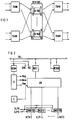
- the switching network according to FIG. 1 also has a space coupling part, to which a plurality of modules SC160 to SC163 belong, which are combined to form an assembly SSM16B.
- the SC160 to SC163 circuit modules are room level modules with 16 inputs and 16 outputs each.
- the assembly SSM16B is arranged between the mentioned time-side coupling units TSMB on the input side and on the output side, with which a switching network is formed in a time-space-time structure.
- the space coupling part is designed in several stages, the individual stages each comprising a plurality of structural units corresponding to the structural unit SSM16B, which, however, depending on the level, have a different number of inputs and outputs than the structural unit SSM16B shown in FIG. 1.
- a circuit module SC16 of FIG. 1 is shown in more detail in FIG. 2, but is only shown to the extent that this is necessary to explain the method according to the invention.
- This circuit module represents a room level unit with 16 inputs SLR0 to SLR15 and 16 outputs SLT0 to SLT15. As actual switching elements for connection These inputs and outputs serve multiplexers MUXS0 to MUXS15, which are each individually assigned to one of the outputs SLT0 to SLT15 and whose 16 inputs are each connected to the same inputs of the other multiplexers.
- a coupling memory CM contains control addresses for the multiplexers MUX0 to MUX15 in the memory locations assigned to the individual time slots of the multiplex system, on the basis of which these establish a connection of one of their inputs with their output for the duration of a time slot consisting of 8 cycles.
- the coupling memory CM is in turn cyclically controlled by a counter C.
- control addresses are transferred to the coupling memory CM each time a new connection is set up from a data input register RDTI.
- the processes of the circuit module shown are controlled by a sequence controller, the registers of the module such as the mentioned register RDTI, the memory CM and the multiplexers MUXS0 to MUXS15 are influenced.
- the corresponding commands originating from a higher-level control are taken from the sequence control for this purpose from a command transfer register RCOM.
- the commands and data mentioned are fed to the module via a bidirectionally operated data bus DB.
- the connections of the registers to this data bus as well as connections for the voltage supply, indicated here by VCC and GND, are part of an interface of the module to which the module is connected to the the building block mentioned belongs, the corresponding connections are made.
- the interface connections leading to registers are such that, if a module is not inserted at all, there are voltage relationships at these connections which correspond to the binary value 1 of digital information.
- bits of the binary value 0 are entered in all positions in the course of resets for the production of defined initial states in the registers.
- each of the circuit components is now assigned an identity register RCHID, which can be both written and read from the bus DB mentioned, in contrast to the mentioned and other registers of the module that are not mentioned and which can only be written or only read.
- a specific address of the module and a specific address of the module to which the module belongs are entered in these registers RCHID, with either the module address or the module address being inverted before writing.
- the registers RCHID are queried via the data bus DB and their content is monitored for compliance with the expected address.
Landscapes
- Engineering & Computer Science (AREA)
- Theoretical Computer Science (AREA)
- Quality & Reliability (AREA)
- Physics & Mathematics (AREA)
- General Engineering & Computer Science (AREA)
- General Physics & Mathematics (AREA)
- Test And Diagnosis Of Digital Computers (AREA)
- Data Exchanges In Wide-Area Networks (AREA)
- Use Of Switch Circuits For Exchanges And Methods Of Control Of Multiplex Exchanges (AREA)
Applications Claiming Priority (2)
| Application Number | Priority Date | Filing Date | Title |
|---|---|---|---|
| DE4333337 | 1993-09-29 | ||
| DE4333337 | 1993-09-29 |
Publications (3)
| Publication Number | Publication Date |
|---|---|
| EP0645703A2 true EP0645703A2 (fr) | 1995-03-29 |
| EP0645703A3 EP0645703A3 (fr) | 1997-09-17 |
| EP0645703B1 EP0645703B1 (fr) | 2001-11-28 |
Family
ID=6499074
Family Applications (1)
| Application Number | Title | Priority Date | Filing Date |
|---|---|---|---|
| EP94114452A Expired - Lifetime EP0645703B1 (fr) | 1993-09-29 | 1994-09-14 | Procédé de vérification du raccordement correct de modules de circuits intégrés |
Country Status (6)
| Country | Link |
|---|---|
| EP (1) | EP0645703B1 (fr) |
| AT (1) | ATE209795T1 (fr) |
| DE (1) | DE59409975D1 (fr) |
| DK (1) | DK0645703T3 (fr) |
| ES (1) | ES2169058T3 (fr) |
| PT (1) | PT645703E (fr) |
Family Cites Families (3)
| Publication number | Priority date | Publication date | Assignee | Title |
|---|---|---|---|---|
| JPS573121A (en) * | 1980-06-07 | 1982-01-08 | Omron Tateisi Electronics Co | Detection system for voltage lowering of memory protecting battery |
| JPS61105659A (ja) * | 1984-10-29 | 1986-05-23 | Oki Electric Ind Co Ltd | 情報処理システム |
| GB2202062B (en) * | 1987-03-14 | 1991-05-01 | Plessey Co Plc | Apparatus for checking a system configuration |
-
1994
- 1994-09-14 AT AT94114452T patent/ATE209795T1/de not_active IP Right Cessation
- 1994-09-14 DK DK94114452T patent/DK0645703T3/da active
- 1994-09-14 ES ES94114452T patent/ES2169058T3/es not_active Expired - Lifetime
- 1994-09-14 DE DE59409975T patent/DE59409975D1/de not_active Expired - Fee Related
- 1994-09-14 PT PT94114452T patent/PT645703E/pt unknown
- 1994-09-14 EP EP94114452A patent/EP0645703B1/fr not_active Expired - Lifetime
Also Published As
| Publication number | Publication date |
|---|---|
| DE59409975D1 (de) | 2002-01-10 |
| ES2169058T3 (es) | 2002-07-01 |
| DK0645703T3 (da) | 2002-04-02 |
| ATE209795T1 (de) | 2001-12-15 |
| EP0645703A3 (fr) | 1997-09-17 |
| EP0645703B1 (fr) | 2001-11-28 |
| PT645703E (pt) | 2002-05-31 |
Similar Documents
| Publication | Publication Date | Title |
|---|---|---|
| DE2726753C2 (de) | Ferngesteuerter Prüf-Interface-Adapter | |
| DE3300260C2 (fr) | ||
| DE69722897T2 (de) | Automatische Adressenzuweisung für Plattenlaufwerke enthaltende Gestelle sowie Fehlererkennungsverfahren und Gerät | |
| DE20009207U1 (de) | Einrichtung zur Signalübertragung | |
| DE3111555C2 (de) | Verfahren und Vorrichtung zur Informationsspeicherung unter Anwendung früherer Aufzeichnung | |
| DE3247801C2 (fr) | ||
| DE2210426B1 (de) | Verfahren zur vorranggesteuerten Auswahl einer von mehreren Funktionseinheiten zur Anschaltung an eine ihnen gemeinsam zugeordnete Einrichtung in Datenverarbeitungsanlagen und Schaltung zur Durchführung des Verfahrens | |
| DE4026581C2 (fr) | ||
| WO1994012936A1 (fr) | Dispositif pour la transmission de donnees au moyen d'un bus | |
| DE3238826A1 (de) | Steuereinheit fuer die eingabe/ausgabe-interface-schaltungen eines rechners | |
| DE3828289C2 (fr) | ||
| DE2708244B2 (de) | Anordnung und Verfahren zur Steuerung eines Vermittlungssystems mit einer Gruppe von Kleinrechnern | |
| EP0645703B1 (fr) | Procédé de vérification du raccordement correct de modules de circuits intégrés | |
| DE10307027A1 (de) | Verfahren und Testeinrichtung zum Ermitteln einer Reparaturlösung für einen Speicherbaustein | |
| EP0388798A1 (fr) | Dispositif pour emmagasiner l'adresse d'une unité processeur de surveillance en service | |
| DE3531901C2 (fr) | ||
| EP0162270B1 (fr) | Méthode pour tester des chemins commutés d'un réseau de connexion multiplex à division dans l'espace | |
| DE3928998A1 (de) | Speicherprogrammierbare steuerung | |
| DE3843564A1 (de) | Verfahren zur ueberpruefung von verbindungs- und/oder schalteinrichtungen und/oder -leitungen | |
| DE4107007A1 (de) | Elektronisches geraet | |
| DE1941265C3 (de) | Speicherprogrammierte Sonderdienst- Zusatzeinrichtung für eine Fernmeldevermittlungsanlage, insbesondere Fernsprechvermittlungsanlage | |
| DE2524957C3 (de) | Anordnung zur Auswahl von Ein- und Ausgabeeinheiten mittels Adressen | |
| EP0003744B1 (fr) | Mémoire centrale composée de mémoires de types différents | |
| DE4303048A1 (en) | Alarm recognition apparatus for redundant layout circuit in radio equipment - has input circuits delaying alarm recognition signals when circuits are switched to be operational systems | |
| DE3248276C2 (fr) |
Legal Events
| Date | Code | Title | Description |
|---|---|---|---|
| PUAI | Public reference made under article 153(3) epc to a published international application that has entered the european phase |
Free format text: ORIGINAL CODE: 0009012 |
|
| AK | Designated contracting states |
Kind code of ref document: A2 Designated state(s): AT BE CH DE DK ES FR GB GR IE IT LI NL PT SE |
|
| PUAL | Search report despatched |
Free format text: ORIGINAL CODE: 0009013 |
|
| AK | Designated contracting states |
Kind code of ref document: A3 Designated state(s): AT BE CH DE DK ES FR GB GR IE IT LI NL PT SE |
|
| 17P | Request for examination filed |
Effective date: 19971006 |
|
| 17Q | First examination report despatched |
Effective date: 19991203 |
|
| GRAG | Despatch of communication of intention to grant |
Free format text: ORIGINAL CODE: EPIDOS AGRA |
|
| GRAG | Despatch of communication of intention to grant |
Free format text: ORIGINAL CODE: EPIDOS AGRA |
|
| GRAH | Despatch of communication of intention to grant a patent |
Free format text: ORIGINAL CODE: EPIDOS IGRA |
|
| GRAH | Despatch of communication of intention to grant a patent |
Free format text: ORIGINAL CODE: EPIDOS IGRA |
|
| GRAA | (expected) grant |
Free format text: ORIGINAL CODE: 0009210 |
|
| AK | Designated contracting states |
Kind code of ref document: B1 Designated state(s): AT BE CH DE DK ES FR GB GR IE IT LI NL PT SE |
|
| REF | Corresponds to: |
Ref document number: 209795 Country of ref document: AT Date of ref document: 20011215 Kind code of ref document: T |
|
| REG | Reference to a national code |
Ref country code: CH Ref legal event code: NV Representative=s name: SIEMENS SCHWEIZ AG Ref country code: CH Ref legal event code: EP |
|
| REG | Reference to a national code |
Ref country code: IE Ref legal event code: FG4D Free format text: GERMAN |
|
| REG | Reference to a national code |
Ref country code: GB Ref legal event code: IF02 |
|
| REF | Corresponds to: |
Ref document number: 59409975 Country of ref document: DE Date of ref document: 20020110 |
|
| GBT | Gb: translation of ep patent filed (gb section 77(6)(a)/1977) |
Effective date: 20020216 |
|
| REG | Reference to a national code |
Ref country code: DK Ref legal event code: T3 |
|
| ET | Fr: translation filed | ||
| REG | Reference to a national code |
Ref country code: PT Ref legal event code: SC4A Free format text: AVAILABILITY OF NATIONAL TRANSLATION Effective date: 20020227 |
|
| REG | Reference to a national code |
Ref country code: ES Ref legal event code: FG2A Ref document number: 2169058 Country of ref document: ES Kind code of ref document: T3 |
|
| REG | Reference to a national code |
Ref country code: GR Ref legal event code: EP Ref document number: 20020400804 Country of ref document: GR |
|
| PLBE | No opposition filed within time limit |
Free format text: ORIGINAL CODE: 0009261 |
|
| STAA | Information on the status of an ep patent application or granted ep patent |
Free format text: STATUS: NO OPPOSITION FILED WITHIN TIME LIMIT |
|
| 26N | No opposition filed | ||
| PGFP | Annual fee paid to national office [announced via postgrant information from national office to epo] |
Ref country code: IE Payment date: 20040810 Year of fee payment: 11 |
|
| PGFP | Annual fee paid to national office [announced via postgrant information from national office to epo] |
Ref country code: DK Payment date: 20040909 Year of fee payment: 11 |
|
| PGFP | Annual fee paid to national office [announced via postgrant information from national office to epo] |
Ref country code: PT Payment date: 20050830 Year of fee payment: 12 |
|
| PGFP | Annual fee paid to national office [announced via postgrant information from national office to epo] |
Ref country code: NL Payment date: 20050905 Year of fee payment: 12 |
|
| PGFP | Annual fee paid to national office [announced via postgrant information from national office to epo] |
Ref country code: GB Payment date: 20050906 Year of fee payment: 12 Ref country code: SE Payment date: 20050906 Year of fee payment: 12 |
|
| PGFP | Annual fee paid to national office [announced via postgrant information from national office to epo] |
Ref country code: AT Payment date: 20050907 Year of fee payment: 12 |
|
| PGFP | Annual fee paid to national office [announced via postgrant information from national office to epo] |
Ref country code: FR Payment date: 20050912 Year of fee payment: 12 |
|
| PG25 | Lapsed in a contracting state [announced via postgrant information from national office to epo] |
Ref country code: IE Free format text: LAPSE BECAUSE OF NON-PAYMENT OF DUE FEES Effective date: 20050914 |
|
| PGFP | Annual fee paid to national office [announced via postgrant information from national office to epo] |
Ref country code: GR Payment date: 20050914 Year of fee payment: 12 Ref country code: BE Payment date: 20050914 Year of fee payment: 12 |
|
| PGFP | Annual fee paid to national office [announced via postgrant information from national office to epo] |
Ref country code: ES Payment date: 20050920 Year of fee payment: 12 |
|
| PG25 | Lapsed in a contracting state [announced via postgrant information from national office to epo] |
Ref country code: DK Free format text: LAPSE BECAUSE OF NON-PAYMENT OF DUE FEES Effective date: 20050930 |
|
| PGFP | Annual fee paid to national office [announced via postgrant information from national office to epo] |
Ref country code: CH Payment date: 20051209 Year of fee payment: 12 |
|
| REG | Reference to a national code |
Ref country code: IE Ref legal event code: MM4A |
|
| PG25 | Lapsed in a contracting state [announced via postgrant information from national office to epo] |
Ref country code: AT Free format text: LAPSE BECAUSE OF NON-PAYMENT OF DUE FEES Effective date: 20060914 |
|
| PG25 | Lapsed in a contracting state [announced via postgrant information from national office to epo] |
Ref country code: SE Free format text: LAPSE BECAUSE OF NON-PAYMENT OF DUE FEES Effective date: 20060915 |
|
| PG25 | Lapsed in a contracting state [announced via postgrant information from national office to epo] |
Ref country code: LI Free format text: LAPSE BECAUSE OF NON-PAYMENT OF DUE FEES Effective date: 20060930 Ref country code: CH Free format text: LAPSE BECAUSE OF NON-PAYMENT OF DUE FEES Effective date: 20060930 Ref country code: BE Free format text: LAPSE BECAUSE OF NON-PAYMENT OF DUE FEES Effective date: 20060930 |
|
| PGFP | Annual fee paid to national office [announced via postgrant information from national office to epo] |
Ref country code: IT Payment date: 20060930 Year of fee payment: 13 |
|
| REG | Reference to a national code |
Ref country code: DK Ref legal event code: EBP |
|
| PG25 | Lapsed in a contracting state [announced via postgrant information from national office to epo] |
Ref country code: PT Free format text: LAPSE BECAUSE OF NON-PAYMENT OF DUE FEES Effective date: 20070314 |
|
| REG | Reference to a national code |
Ref country code: PT Ref legal event code: MM4A Free format text: LAPSE DUE TO NON-PAYMENT OF FEES Effective date: 20070314 |
|
| PG25 | Lapsed in a contracting state [announced via postgrant information from national office to epo] |
Ref country code: NL Free format text: LAPSE BECAUSE OF NON-PAYMENT OF DUE FEES Effective date: 20070401 |
|
| REG | Reference to a national code |
Ref country code: CH Ref legal event code: PL |
|
| EUG | Se: european patent has lapsed | ||
| GBPC | Gb: european patent ceased through non-payment of renewal fee |
Effective date: 20060914 |
|
| NLV4 | Nl: lapsed or anulled due to non-payment of the annual fee |
Effective date: 20070401 |
|
| REG | Reference to a national code |
Ref country code: FR Ref legal event code: ST Effective date: 20070531 |
|
| PGFP | Annual fee paid to national office [announced via postgrant information from national office to epo] |
Ref country code: DE Payment date: 20070921 Year of fee payment: 14 |
|
| PG25 | Lapsed in a contracting state [announced via postgrant information from national office to epo] |
Ref country code: GB Free format text: LAPSE BECAUSE OF NON-PAYMENT OF DUE FEES Effective date: 20060914 |
|
| REG | Reference to a national code |
Ref country code: ES Ref legal event code: FD2A Effective date: 20060915 |
|
| BERE | Be: lapsed |
Owner name: *SIEMENS A.G. Effective date: 20060930 |
|
| PG25 | Lapsed in a contracting state [announced via postgrant information from national office to epo] |
Ref country code: ES Free format text: LAPSE BECAUSE OF NON-PAYMENT OF DUE FEES Effective date: 20060915 |
|
| PG25 | Lapsed in a contracting state [announced via postgrant information from national office to epo] |
Ref country code: FR Free format text: LAPSE BECAUSE OF NON-PAYMENT OF DUE FEES Effective date: 20061002 |
|
| PG25 | Lapsed in a contracting state [announced via postgrant information from national office to epo] |
Ref country code: GR Free format text: LAPSE BECAUSE OF NON-PAYMENT OF DUE FEES Effective date: 20070404 |
|
| PG25 | Lapsed in a contracting state [announced via postgrant information from national office to epo] |
Ref country code: IT Free format text: LAPSE BECAUSE OF NON-PAYMENT OF DUE FEES Effective date: 20070914 Ref country code: DE Free format text: LAPSE BECAUSE OF NON-PAYMENT OF DUE FEES Effective date: 20090401 |