EP0647063A1 - Contrôle électronique de la durée d'exposition - Google Patents
Contrôle électronique de la durée d'exposition Download PDFInfo
- Publication number
- EP0647063A1 EP0647063A1 EP94307239A EP94307239A EP0647063A1 EP 0647063 A1 EP0647063 A1 EP 0647063A1 EP 94307239 A EP94307239 A EP 94307239A EP 94307239 A EP94307239 A EP 94307239A EP 0647063 A1 EP0647063 A1 EP 0647063A1
- Authority
- EP
- European Patent Office
- Prior art keywords
- signal
- image
- iris
- exposure
- operable
- Prior art date
- Legal status (The legal status is an assumption and is not a legal conclusion. Google has not performed a legal analysis and makes no representation as to the accuracy of the status listed.)
- Granted
Links
- 230000007704 transition Effects 0.000 claims description 37
- 230000008859 change Effects 0.000 claims description 22
- 238000000034 method Methods 0.000 claims description 19
- 230000003247 decreasing effect Effects 0.000 claims description 5
- 230000004075 alteration Effects 0.000 claims description 3
- 238000012544 monitoring process Methods 0.000 abstract 1
- 230000006870 function Effects 0.000 description 7
- 230000008569 process Effects 0.000 description 6
- 206010065042 Immune reconstitution inflammatory syndrome Diseases 0.000 description 4
- 238000010586 diagram Methods 0.000 description 4
- 230000004044 response Effects 0.000 description 3
- 238000010894 electron beam technology Methods 0.000 description 2
- 230000006378 damage Effects 0.000 description 1
- 230000000694 effects Effects 0.000 description 1
- 230000000737 periodic effect Effects 0.000 description 1
- 239000004065 semiconductor Substances 0.000 description 1
- 239000007787 solid Substances 0.000 description 1
- 238000006467 substitution reaction Methods 0.000 description 1
- 239000013589 supplement Substances 0.000 description 1
Images

Classifications
-
- H—ELECTRICITY
- H04—ELECTRIC COMMUNICATION TECHNIQUE
- H04N—PICTORIAL COMMUNICATION, e.g. TELEVISION
- H04N25/00—Circuitry of solid-state image sensors [SSIS]; Control thereof
- H04N25/50—Control of the SSIS exposure
- H04N25/53—Control of the integration time
-
- H—ELECTRICITY
- H04—ELECTRIC COMMUNICATION TECHNIQUE
- H04N—PICTORIAL COMMUNICATION, e.g. TELEVISION
- H04N23/00—Cameras or camera modules comprising electronic image sensors; Control thereof
- H04N23/70—Circuitry for compensating brightness variation in the scene
- H04N23/73—Circuitry for compensating brightness variation in the scene by influencing the exposure time
-
- H—ELECTRICITY
- H04—ELECTRIC COMMUNICATION TECHNIQUE
- H04N—PICTORIAL COMMUNICATION, e.g. TELEVISION
- H04N25/00—Circuitry of solid-state image sensors [SSIS]; Control thereof
- H04N25/70—SSIS architectures; Circuits associated therewith
- H04N25/71—Charge-coupled device [CCD] sensors; Charge-transfer registers specially adapted for CCD sensors
- H04N25/745—Circuitry for generating timing or clock signals
Definitions
- This invention relates in general to the field of electronic systems and more particularly to an improved video processing system.
- Electronic iris controllers have been developed to eliminate the need for or supplement a mechanical iris to control the amount of light that impinges on a solid state electronic image sensor.
- An electronic iris controls the exposure time by periodically exposing or removing the charge generated by the photon-generated hole-electron pairs within the image sensor. This process of periodic destruction or removal of charge is referred to as the clearing of the image sensor.
- the charge is also removed from the image sensor when the signal from the image sensor is transferred to an image memory associated with the image sensor. This process is referred to as the image transfer.
- the length of time between the clearing of the image and the transfer of the image sets the electronic exposure time. By altering the relative positions of the image clear operation and the image transfer operation, the length of exposure time can be controlled electronically.
- the image memory is capacitively coupled to the image sensor. Accordingly, during the readout of information from the image memory, no other operations are performed on the image sensor or the image memory to minimize interference with the readout sequence.
- the maximum exposure time for a field of data is 16.67 milliseconds.
- a typical field of television data comprises 262.5 lines of information.
- an electronic iris controller that provides for exposure control in a more linear fashion.
- an electronic iris controller is provided that substantially eliminates or reduces disadvantages and problems associated with prior systems.
- a video processing system comprising an electronic iris controller operable to alter an exposure time associated with the system in sequential increments.
- the system further comprises an image sensor and an image memory operable to generate and store image data.
- the electronic iris controller is operable to output an image clear signal and an image transfer signal that determines the exposure time of the image.
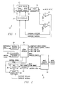
- a video processing system indicated generally at 10 is shown to comprise a lens 12 which focuses light on an image area 14 of an image sensor 15. Periodically, image data is transferred from the image area 14 to an image memory 18.
- the video processor 16 retrieves the image data from image memory 18 and outputs it as a VIDEO OUTPUT signal.
- the VIDEO OUTPUT signal is also routed to a first comparator 20 and a second comparator 22.
- the first comparator 20 compares the average level of the VIDEO OUTPUT signal to a first reference voltage V1.
- the second comparator 22 compares the average level of the VIDEO OUTPUT signal to a second reference voltage V2.
- comparator 20 When the average of the VIDEO OUTPUT signal falls below the reference level V1, the exposure of the image needs to be increased. Accordingly, comparator 20 outputs an EXPOSURE INCREASE signal to an iris controller circuit 24. Similarly, if the average level of the VIDEO OUTPUT signal rises above the reference level V2, the exposure of the image must be decreased. The comparator 22, therefore, outputs an EXPOSURE DECREASE signal to iris controller 24.
- the iris controller 24 outputs signals to the image sensor image area 14 and to the image memory 18. Iris controller 24 operates, in part, to control two functions of the image sensor image area 14 and image memory 18. The image sensor image area 14 periodically transfers the image to the image memory 18.
- the transfer of data from the image sensor image area 14 to the image memory 18 destroys the charge stored in the image sensor image area 14.
- the charge in image sensor image area 14 is created by photon-generated electron-hole pairs within the semiconductor image sensor image area 14 created by light focused on the image sensor image area 14 through lens 12.
- the iris controller 24 also periodically instructs the image sensor image area 14 to clear the image from image sensor image area 14. This clearing function is also accomplished by draining the charge from the image sensor image area 14 in a similar manner to the method used to transfer the charge to the image memory 18.
- the time between the clearing of the image sensor image area 14 and the transfer of image data from image sensor image area 14 to image memory 18 is the electronic exposure time.
- the iris controller 24 can control the exposure time of the image stored in image sensor image area 14 by controlling the times at which the signals instructing the image sensor image area 14 and the image memory 18 to clear the image sensor image area 14 and to transfer the image data from image sensor image area 14 to image memory 18 occur.
- the image sensor image area 14 and image memory 18 comprise charge-coupled devices which are capacitively coupled to one another. Accordingly, the transfer and clear operations controlled by iris controller 24 cannot be performed while the video processor 16 is reading image data. If these operations are performed during the reading process, the image stored within the image sensor can be disturbed.
- Video images are typically organized as pairs of interlaced fields, each comprising 262.5 lines of image data. These two fields together constitute a single video frame comprising 525 lines.
- the images are read out line-by-line by the video processor 16 from the image memory 18.
- There are two typical varieties of image sensors which may comprise image sensor image area 14 and image memory 18.
- the first variety is a line addressable image sensor where each line is transferred on an individual basis to the image memory 18.
- the second type of image sensor is a frame transfer image sensor. Frame transfer image sensors transfer the entire image to image memory at one time.
- the video processor 16 functions in a similar manner regardless of whether image sensor image area 14 and image memory 18 are line addressable or frame transfer systems.
- the video processor 16 functions to output the video image data on a line-by-line basis through the VIDEO OUTPUT signal.
- the horizontal blanking period is the time it takes for the electron beam to scan horizontally back across the cathode ray tube (CRT) after it has drawn a line of image.
- CRT cathode ray tube
- the vertical blanking period is typically on the order of 1.27 milliseconds in length and constitutes the time required for the electron beam to scan back from the bottom right-hand corner of the CRT display to the top left-hand corner of the CRT display. Similar to the horizontal blanking period, no operations are performed on the data stored in image memory 18 by the video processor 16 during the vertical blanking period. Accordingly, the image clear and image transfer functions can occur at any point within the vertical blanking period.
- the relative position of the image transfer and image clear operations control the electronic exposure of the image on the image sensor 15.
- the only time that the image clear and image transfer functions can occur is either during the horizontal blanking period which occurs once every 63.5 microseconds or any time during the vertical blanking period which occurs twice during a frame of video data at the beginning of each field and lasts approximately 1.2 milliseconds.
- FIGURE 2 illustrates one embodiment of iris controller 24 constructed according to the teachings of the present invention that capitalizes on both the horizontal blanking and the vertical blanking period to implement a floating phase iris controller that enables control of the image sensor 15 to approach linear operation.
- a MASTER CLOCK signal is used to drive a horizontal counter circuit 26.
- the horizontal counter circuit 26 is used to address the horizontal position within a single line of the video image.
- the horizontal counter circuit 26 increments as driven by the MASTER CLOCK signal until it reaches a maximum value and then resets.
- a HORIZONTAL DRIVE signal is created and output to a vertical counter circuit 28.
- the horizontal counter value is output to a signal decoder circuit 30.
- the vertical counter circuit 28 is incremented each time the horizontal counter circuit 26 reaches its maximum value at the end of the line of image data. Accordingly, the vertical counter circuit 28 is incremented each time a horizontal blanking period occurs.
- the value within the vertical counter circuit 28 is also output to signal decoder 30.
- the vertical counter circuit 28 counts to a maximum value which may comprise, for example, 525 or one count for each line in a complete frame of video data. Upon reaching the maximum value, the vertical counter circuit 28 resets and begins counting from one.
- the signal decoder 30 uses the vertical counter value and the horizontal counter value to determine when horizontal blanking and vertical blanking periods occur.
- the IMAGE TRANSFER signal is locked in phase with respect to the MASTER CLOCK and HORIZONTAL DRIVE signals. Accordingly, the signal decoder 30 outputs an image TRANSFER ENABLE signal to an image transfer controller circuit 32 whenever, according to one embodiment of the present invention, the IMAGE TRANSFER signal is transmitted by the signal decoder circuit 30 to the image transfer controller circuit immediately before the end of a vertical blanking period.
- the IMAGE TRANSFER signal locked in phase with the MASTER CLOCK and horizontal counter 26 and vertical counter 28 signal, the exposure of the image sensor can be controlled by adjusting the relative position of the IMAGE CLEAR signal also transmitted to the image transfer controller circuit 32.
- the IMAGE CLEAR signal is created by an iris signal decoder circuit 34 shown in FIGURE 2.
- the iris signal decoder circuit receives a count from an iris counter 36.
- the iris counter 36 increments with each transition of an accordion clock signal (ACLK).
- the ACLK signal is referred to as an accordion clock signal because it is a non-linear clock signal that comprises a constant number of transitions for the time required to process a full frame of video data. However, the transitions of the ACLK signal do not occur in a linear fashion.
- the transitions are of differing duration and may be divided into control zones which will be discussed more completely herein.
- the maximum count for the iris counter is set by a count length set circuit 38 shown in FIGURE 2.
- the count length set circuit 38 receives CONTROL ZONE indicator signals from the signal decoder 30.
- the count length set circuit 38 also receives the EXPOSURE DECREASE and EXPOSURE INCREASE signals from comparators 20 and comparators 22 described with reference to FIGURE 1 previously.
- the exposure time between the IMAGE CLEAR signal and the IMAGE TRANSFER signal is held constant or adjusted by the iris counter 36 and the iris signal decoder 34.
- the iris counter counts to a set number of transitions of the ACLK signal. As long as the maximum count length used by the iris counter 36 remains unchanged, the IMAGE CLEAR signal output by iris signal decoder 34 will remain fixed in phase with respect to the IMAGE TRANSFER signal output by signal decoder 30.
- the exposure time is adjusted by allowing the IMAGE CLEAR signal to float in phase with respect to the IMAGE TRANSFER signal until the exposure length reaches the desired length of time.
- the IMAGE CLEAR signal is cause to float by altering the maximum count length used by iris counter 36 to count the transitions of the ACLK signal.
- the count length is altered by the count length set circuit 38 in response to the EXPOSURE DECREASE signal or the EXPOSURE INCREASE signal.
- the count length is increased by the count length set circuit 38 in order to decrease the exposure length and the count length will be decreased in order to increase the exposure length.
- FIGURE 3 a timing diagram is shown which illustrates the juxtaposition of some of the signals used in the operation of the system of the present invention.
- the first line of FIGURE 3 is a FIELD INDICATOR signal.
- a low value of the field indicator indicates that the first field of the frame is being processed while a high value of the FIELD INDICATOR signal indicates that the second field of the frame is being processed.
- the second line within FIGURE 2 indicates the VERTICAL BLANKING INDICATOR signal.
- the vertical blanking periods as shown occur at the beginning of each field and last for approximately 1.27 milliseconds.
- the next line of FIGURE 3 indicates the IMAGE TRANSFER signal.
- the image transfer signal is a very short duration signal that occurs immediately before the end of the vertical blanking period. As discussed previously, the IMAGE TRANSFER signal allows for the transfer of the image from the image sensor image area 14 into the image memory 18. This transfer takes approximately 10 microseconds.
- the next line of FIGURE 3 illustrates the transitions on the HORIZONTAL DRIVE signal.
- Each vertical line within the representation of the HORIZONTAL DRIVE signal illustrates a transition that occurs simultaneously with a horizontal blanking period.
- the actual duration of the horizontal drive transitions cannot be illustrated.
- An actual transition occurs every 63.5 microseconds and there are 525 transitions between the beginning of field 1 and the end of field 2.
- the HORIZONTAL DRIVE signal is shown with much larger transitions to illustrate the relationship of the HORIZONTAL DRIVE signal with the ACLK signal which follows.
- the iris counter 36 receives the ACLK clock signal from the signal decoder 30 and uses the ACLK signal to trigger its counting operations.
- the iris signal decoder 34 generates the IMAGE CLEAR signal responsive to the value in the iris counter 36. Accordingly, the iris signal decoder 34 and the IMAGE CLEAR signal are effectively clocked off of the ACLK signal.
- the IMAGE CLEAR signal corresponds to a transition of the ACLK signal. If the maximum count value for iris counter 36 is changed by count length set circuit 38, the IMAGE CLEAR signal will float to the next transition of the ACLK signal as indicated in phantom at reference number 42 in FIGURE 3 effectively decreasing the exposure time of the system.
- the location of the IMAGE CLEAR signal for maximum exposure is indicated at reference 40 in FIGURE 3.
- the image clear would float in even increments from one transition of the HORIZONTAL DRIVE signal to the next.
- this method of adjusting the exposure would provide for an even change in the time of the exposure as the phase of the IMAGE CLEAR signal floated with respect to the phase of the IMAGE TRANSFER signal, the percentage change of each incremental change would vary in an extremely non-linear fashion.
- the initial increment from the value of the IMAGE CLEAR signal providing the longest exposure period possible to the next-to-longest period possible comprises approximately a 0.4 percent change.
- the last incremental change from the next-to-shortest to the shortest exposure time possible comprises a 50 percent change in exposure.
- the percentage exposure change should be brought as close to a linear relationship as possible.
- the system of the present invention utilizes two methods for making the exposure change more linear.
- the first method for adjusting the linearity of the exposure change is accomplished by creating the non-linear clock signal ACLK.
- the ACLK signal comprises a constant number of transitions for the length of time necessary for a complete frame of video data. However, the transitions are spaced in an uneven manner to allow for longer transitions during the beginning of the field and extremely short transitions during the vertical blanking period. As discussed previously, the image clear process must occur during either a horizontal blanking period or the vertical blanking period. Accordingly, the transitions of the ACLK signal within, for example, region 44 shown in FIGURE 3 each occur during a horizontal blanking period. Accordingly, the transitions within region 44 cannot occur more often than 63.5 microseconds. This constraint does not apply, however, to the vertical blanking period shown in region 46 in FIGURE 3. Accordingly, the transitions of the ACLK signal may be spaced at any interval within region 46.
- Region 44 can also be subdivided into region 48 and region 50 shown in FIGURE 3.
- the transitions of the ACLK signal within region 48 occur once every two times a horizontal blanking period occurs.
- a transition of the ACLK signal occurs every time a horizontal blanking period occurs.
- the progression of the ACLK signal provides that the incremental floating of the IMAGE CLEAR signal from one transition to another will comprise larger steps in some portions such as regions 48 and 50 of the time base and very fine transitions within other regions of the time base such as region 46. This variability in the transition length increases the linearity of the percentage change in the exposure time.
- the operation of the non-linear clock signal ACLK provides that the change in the exposure time from position 40 to position 42 will represent roughly the same percentage change in the exposure as the change in, for example, position 52 to position 54 shown in FIGURE 3.
- FIGURE 3 also illustrates the IRIS STOP UP signal and the IRIS STOP DOWN signal which are created by signal decoder 30 and prevent the IMAGE CLEAR signal from floating past a predetermined limit as the exposure time is changed. If the IMAGE CLEAR signal was allowed to continue to float, the signal would pass immediately from the shortest exposure setting to the longest exposure setting. The IRIS STOP UP signal and IRIS STOP DOWN signal prevent this from occurring.
- FIGURE 3 also illustrates three exemplary control zone signals, the CONTROL ZONE 1 signal, CONTROL ZONE 2 signal and CONTROL ZONE 3 signal.
- the CONTROL ZONE signals are used by the system of the present invention to accomplish the second method of increasing the linearity of the exposure change of the system.
- the CONTROL ZONE signals indicate to the count length set circuit 38 where the IMAGE CLEAR signal resides within the time base.
- the CONTROL ZONE 1 signal is active within region 48 described previously
- the CONTROL ZONE 2 signal is active during region 50 described previously
- the CONTROL ZONE 3 signal is active during region 46 corresponding to the vertical blanking period.
- the CONTROL ZONE signals are used to provide for changes in the maximum count of iris counter 36 that are greater than one.
- the iris counter 36 can cause the IMAGE CLEAR signal to transition by more than one transition by changing the maximum count by two or more instead of one. Even quicker transitions of the IMAGE CLEAR signal with respect to the IMAGE TRANSFER signal can be accomplished by changing the maximum count of the iris counter 36 by even larger amounts.
- the CONTROL ZONE signals are used to divide the time base into regions such that the combination of the non-linear ACLK clock signal and the use of selective maximum counts for the iris counter can be used to create a more linear percentage exposure change response.
- CONTROL ZONE signals and the transitions of the ACLK signal included in the illustrated embodiment are solely for the purposes of teaching the advantages of the present invention and should not be construed to limit the present invention to this or any exemplary embodiment.
- the CONTROL ZONE signals and ACLK signal transitions can be used in any number of combinations to create whatever exposure response is required.
Landscapes
- Engineering & Computer Science (AREA)
- Multimedia (AREA)
- Signal Processing (AREA)
- Transforming Light Signals Into Electric Signals (AREA)
- Studio Devices (AREA)
- Exposure Control For Cameras (AREA)
Applications Claiming Priority (2)
| Application Number | Priority Date | Filing Date | Title |
|---|---|---|---|
| US13054393A | 1993-10-01 | 1993-10-01 | |
| US130543 | 1993-10-01 |
Publications (2)
| Publication Number | Publication Date |
|---|---|
| EP0647063A1 true EP0647063A1 (fr) | 1995-04-05 |
| EP0647063B1 EP0647063B1 (fr) | 2003-01-29 |
Family
ID=22445181
Family Applications (1)
| Application Number | Title | Priority Date | Filing Date |
|---|---|---|---|
| EP94307239A Expired - Lifetime EP0647063B1 (fr) | 1993-10-01 | 1994-10-03 | Contrôle électronique de la durée d'exposition |
Country Status (7)
| Country | Link |
|---|---|
| US (1) | US6081294A (fr) |
| EP (1) | EP0647063B1 (fr) |
| JP (1) | JPH07255008A (fr) |
| KR (1) | KR100341978B1 (fr) |
| DE (1) | DE69432069T2 (fr) |
| MY (1) | MY112406A (fr) |
| TW (1) | TW302449B (fr) |
Cited By (4)
| Publication number | Priority date | Publication date | Assignee | Title |
|---|---|---|---|---|
| GB2322496A (en) * | 1997-02-14 | 1998-08-26 | Matsushita Electric Industrial Co Ltd | Solid-state video camera exposure and gain control system |
| US5986705A (en) * | 1997-02-18 | 1999-11-16 | Matsushita Electric Industrial Co., Ltd. | Exposure control system controlling a solid state image sensing device |
| WO2000025513A1 (fr) * | 1998-10-23 | 2000-05-04 | Smith & Nephew, Inc. | Optimisation de l'eclairement d'une image |
| DE10309040A1 (de) * | 2003-03-01 | 2004-09-09 | Volkswagen Ag | Verfahren und Vorrichtung zur Belichtungszeitoptimierung |
Families Citing this family (7)
| Publication number | Priority date | Publication date | Assignee | Title |
|---|---|---|---|---|
| US7268809B2 (en) * | 1998-09-23 | 2007-09-11 | San Disk Corporation | Analog buffer memory for high-speed digital image capture |
| JP3913388B2 (ja) * | 1999-02-01 | 2007-05-09 | 三洋電機株式会社 | 固体撮像装置 |
| US6946635B1 (en) * | 2000-10-05 | 2005-09-20 | Ess Technology, Inc. | System for improving the dynamic range of solid-state imaging devices |
| JP2002298132A (ja) * | 2001-04-02 | 2002-10-11 | Fuji Mach Mfg Co Ltd | 撮像システム,撮像システム制御プログラムおよび電気部品装着システム |
| US7027092B2 (en) * | 2001-09-17 | 2006-04-11 | Hewlett-Packard Development Company, L.P. | Image capture and storage device |
| TWI235961B (en) * | 2004-02-02 | 2005-07-11 | Via Tech Inc | Method for transmitting image frame |
| JP4867552B2 (ja) * | 2006-09-28 | 2012-02-01 | 株式会社ニコン | 撮像装置 |
Citations (4)
| Publication number | Priority date | Publication date | Assignee | Title |
|---|---|---|---|---|
| US5040070A (en) * | 1989-10-17 | 1991-08-13 | Sanyo Electric Co., Ltd. | Solid-state image sensing apparatus for electronically controlling exposure by employing CCD as solid-state image sensing device and method of driving such CCD |
| US5233428A (en) * | 1991-11-05 | 1993-08-03 | Loral Fairchild Systems | Electronic exposure control system for a solid state imager |
| EP0583143A2 (fr) * | 1992-08-10 | 1994-02-16 | Sony Corporation | Amélioration du contrôle du temps d'un obturateur électronique dans une caméra vidéo |
| JPH06113194A (ja) * | 1992-08-10 | 1994-04-22 | Sony Corp | 固体撮像装置の駆動方法とビデオカメラの電子アイリス制御回路 |
Family Cites Families (9)
| Publication number | Priority date | Publication date | Assignee | Title |
|---|---|---|---|---|
| US4051353A (en) * | 1976-06-30 | 1977-09-27 | International Business Machines Corporation | Accordion shift register and its application in the implementation of level sensitive logic system |
| JPS6074878A (ja) * | 1983-09-30 | 1985-04-27 | Canon Inc | 光電変換器の蓄積時間補正装置 |
| JPS6165577A (ja) * | 1984-09-05 | 1986-04-04 | Fuji Photo Film Co Ltd | 画像情報読取方法 |
| KR900000331B1 (ko) * | 1985-02-20 | 1990-01-25 | 마쯔시다덴기산교 가부시기가이샤 | 비데오 카메라장치 |
| US4769710A (en) * | 1985-10-06 | 1988-09-06 | Fuji Photo Film Co., Ltd. | Method for controlling accumulation type photoelectric conversion element |
| JPH02134989A (ja) * | 1988-11-15 | 1990-05-23 | Sanyo Electric Co Ltd | 固体撮像装置 |
| JP2920924B2 (ja) * | 1989-01-12 | 1999-07-19 | ソニー株式会社 | Ccdカメラ |
| ATE181629T1 (de) * | 1990-04-23 | 1999-07-15 | Canon Kk | Photoelektrische wandlungsvorrichtung |
| JPH04119776A (ja) * | 1990-09-11 | 1992-04-21 | Sony Corp | 固体撮像装置 |
-
1994
- 1994-09-29 MY MYPI94002589A patent/MY112406A/en unknown
- 1994-10-01 KR KR1019940025228A patent/KR100341978B1/ko not_active Expired - Lifetime
- 1994-10-03 EP EP94307239A patent/EP0647063B1/fr not_active Expired - Lifetime
- 1994-10-03 DE DE69432069T patent/DE69432069T2/de not_active Expired - Lifetime
- 1994-10-03 JP JP6275469A patent/JPH07255008A/ja active Pending
- 1994-12-16 TW TW083112019A patent/TW302449B/zh not_active IP Right Cessation
-
1996
- 1996-04-03 US US08/627,838 patent/US6081294A/en not_active Expired - Lifetime
Patent Citations (4)
| Publication number | Priority date | Publication date | Assignee | Title |
|---|---|---|---|---|
| US5040070A (en) * | 1989-10-17 | 1991-08-13 | Sanyo Electric Co., Ltd. | Solid-state image sensing apparatus for electronically controlling exposure by employing CCD as solid-state image sensing device and method of driving such CCD |
| US5233428A (en) * | 1991-11-05 | 1993-08-03 | Loral Fairchild Systems | Electronic exposure control system for a solid state imager |
| EP0583143A2 (fr) * | 1992-08-10 | 1994-02-16 | Sony Corporation | Amélioration du contrôle du temps d'un obturateur électronique dans une caméra vidéo |
| JPH06113194A (ja) * | 1992-08-10 | 1994-04-22 | Sony Corp | 固体撮像装置の駆動方法とビデオカメラの電子アイリス制御回路 |
Non-Patent Citations (2)
| Title |
|---|
| MOCHIZUKI ET AL.: "A NEW TIMING CONTROL IC FOR CCD CAMERA SYSTEM", INTERNATIONAL CONFERENCE ON CONSUMER ELECTRONICS DIGEST OF TECHNICAL PAPERS, 8 June 1993 (1993-06-08), ROSEMONT, IL., USA, pages 162 - 163, XP000427569 * |
| PATENT ABSTRACTS OF JAPAN vol. 18, no. 397 (E - 1583) 26 July 1994 (1994-07-26) * |
Cited By (7)
| Publication number | Priority date | Publication date | Assignee | Title |
|---|---|---|---|---|
| GB2322496A (en) * | 1997-02-14 | 1998-08-26 | Matsushita Electric Industrial Co Ltd | Solid-state video camera exposure and gain control system |
| GB2322496B (en) * | 1997-02-14 | 2001-08-08 | Matsushita Electric Industrial Co Ltd | Exposure control system |
| DE19705748B4 (de) * | 1997-02-14 | 2006-06-29 | Matsushita Electric Industrial Co., Ltd., Kadoma | Belichtungs-Steuervorrichtung |
| US5986705A (en) * | 1997-02-18 | 1999-11-16 | Matsushita Electric Industrial Co., Ltd. | Exposure control system controlling a solid state image sensing device |
| WO2000025513A1 (fr) * | 1998-10-23 | 2000-05-04 | Smith & Nephew, Inc. | Optimisation de l'eclairement d'une image |
| AU773992B2 (en) * | 1998-10-23 | 2004-06-10 | Smith & Nephew, Inc. | Image illumination optimizing |
| DE10309040A1 (de) * | 2003-03-01 | 2004-09-09 | Volkswagen Ag | Verfahren und Vorrichtung zur Belichtungszeitoptimierung |
Also Published As
| Publication number | Publication date |
|---|---|
| TW302449B (fr) | 1997-04-11 |
| MY112406A (en) | 2001-06-30 |
| DE69432069D1 (de) | 2003-03-06 |
| DE69432069T2 (de) | 2003-07-10 |
| EP0647063B1 (fr) | 2003-01-29 |
| KR950012267A (ko) | 1995-05-16 |
| US6081294A (en) | 2000-06-27 |
| JPH07255008A (ja) | 1995-10-03 |
| KR100341978B1 (ko) | 2002-11-23 |
Similar Documents
| Publication | Publication Date | Title |
|---|---|---|
| US6081294A (en) | Video processing system | |
| USRE41454E1 (en) | Camera having an adaptive gain control | |
| US8514310B2 (en) | Increasing readout speed in CMOS APS sensors through group readout | |
| US6423957B1 (en) | CMOS image sensor having automatic reference voltage controller | |
| US4644405A (en) | Method and apparatus for scanning a window in the image zone of a charge transfer device of the frame transfer type | |
| US5894325A (en) | Solid image pickup unit and video camera employing same | |
| PT95091A (pt) | Arranjo de controlo de convergencia para formatos verticais multiplos e aparelho de televisao incluindo o arranjo | |
| US4791308A (en) | Solid-state image pick-up apparatus having variable magnification of image sizes by changing the image sensor address range | |
| EP0222508A1 (fr) | Commande de niveau d'un signal vidéo | |
| EP0942594B1 (fr) | Dispositif de prise de vues à l'état solide | |
| GB2329959A (en) | Active pixel sensor with electronic shutter | |
| US5576762A (en) | Solid-state image pickup device | |
| US4723169A (en) | Image pickup apparatus having coordinated clamping and anti-blooming means | |
| NZ202885A (en) | Digital signal gain control arramgement | |
| US4509074A (en) | Television installation comprising a circuit arrangement for the compensation of amplitude variations | |
| EP0353803A1 (fr) | Circuit pour le traitement de signaux vidéo | |
| DE69420779T2 (de) | Videokamera und Verfahren zum Steuern der Videokamera | |
| US4943861A (en) | Apparatus and method for exposing photosensitive recording media with digital image data | |
| EP0234884A2 (fr) | Arrangements d'affichage de tube à rayons cathodique | |
| DE69028383T2 (de) | Schaltung zur automatischen Regelung des Weiss- und Schwarzabgleiches und deren Verfahren | |
| US4922328A (en) | Velocity controlled CRT auto tracking system | |
| US7830438B2 (en) | Frame shuttering scheme for increased frame rate | |
| CA2062600A1 (fr) | Circuit de correction du papillotement | |
| KR100747875B1 (ko) | 능동 픽셀 센서 회로 | |
| WO2002063869A1 (fr) | Reglages de parametres d'imagerie a la volee |
Legal Events
| Date | Code | Title | Description |
|---|---|---|---|
| PUAI | Public reference made under article 153(3) epc to a published international application that has entered the european phase |
Free format text: ORIGINAL CODE: 0009012 |
|
| AK | Designated contracting states |
Kind code of ref document: A1 Designated state(s): DE FR GB IT NL |
|
| 17P | Request for examination filed |
Effective date: 19951002 |
|
| 17Q | First examination report despatched |
Effective date: 19990308 |
|
| GRAG | Despatch of communication of intention to grant |
Free format text: ORIGINAL CODE: EPIDOS AGRA |
|
| GRAG | Despatch of communication of intention to grant |
Free format text: ORIGINAL CODE: EPIDOS AGRA |
|
| GRAH | Despatch of communication of intention to grant a patent |
Free format text: ORIGINAL CODE: EPIDOS IGRA |
|
| GRAH | Despatch of communication of intention to grant a patent |
Free format text: ORIGINAL CODE: EPIDOS IGRA |
|
| GRAA | (expected) grant |
Free format text: ORIGINAL CODE: 0009210 |
|
| AK | Designated contracting states |
Designated state(s): DE FR GB IT NL |
|
| PG25 | Lapsed in a contracting state [announced via postgrant information from national office to epo] |
Ref country code: NL Free format text: LAPSE BECAUSE OF FAILURE TO SUBMIT A TRANSLATION OF THE DESCRIPTION OR TO PAY THE FEE WITHIN THE PRESCRIBED TIME-LIMIT Effective date: 20030129 Ref country code: IT Free format text: LAPSE BECAUSE OF FAILURE TO SUBMIT A TRANSLATION OF THE DESCRIPTION OR TO PAY THE FEE WITHIN THE PRESCRIBED TIME-LIMIT;WARNING: LAPSES OF ITALIAN PATENTS WITH EFFECTIVE DATE BEFORE 2007 MAY HAVE OCCURRED AT ANY TIME BEFORE 2007. THE CORRECT EFFECTIVE DATE MAY BE DIFFERENT FROM THE ONE RECORDED. Effective date: 20030129 |
|
| REG | Reference to a national code |
Ref country code: GB Ref legal event code: FG4D |
|
| REF | Corresponds to: |
Ref document number: 69432069 Country of ref document: DE Date of ref document: 20030306 Kind code of ref document: P |
|
| NLV1 | Nl: lapsed or annulled due to failure to fulfill the requirements of art. 29p and 29m of the patents act | ||
| ET | Fr: translation filed | ||
| PLBE | No opposition filed within time limit |
Free format text: ORIGINAL CODE: 0009261 |
|
| STAA | Information on the status of an ep patent application or granted ep patent |
Free format text: STATUS: NO OPPOSITION FILED WITHIN TIME LIMIT |
|
| 26N | No opposition filed |
Effective date: 20031030 |
|
| PGFP | Annual fee paid to national office [announced via postgrant information from national office to epo] |
Ref country code: GB Payment date: 20090914 Year of fee payment: 16 |
|
| PGFP | Annual fee paid to national office [announced via postgrant information from national office to epo] |
Ref country code: DE Payment date: 20091030 Year of fee payment: 16 |
|
| PGFP | Annual fee paid to national office [announced via postgrant information from national office to epo] |
Ref country code: FR Payment date: 20091020 Year of fee payment: 16 |
|
| GBPC | Gb: european patent ceased through non-payment of renewal fee |
Effective date: 20101003 |
|
| PG25 | Lapsed in a contracting state [announced via postgrant information from national office to epo] |
Ref country code: FR Free format text: LAPSE BECAUSE OF NON-PAYMENT OF DUE FEES Effective date: 20101102 |
|
| REG | Reference to a national code |
Ref country code: FR Ref legal event code: ST Effective date: 20110630 |
|
| PG25 | Lapsed in a contracting state [announced via postgrant information from national office to epo] |
Ref country code: GB Free format text: LAPSE BECAUSE OF NON-PAYMENT OF DUE FEES Effective date: 20101003 |
|
| REG | Reference to a national code |
Ref country code: DE Ref legal event code: R119 Ref document number: 69432069 Country of ref document: DE Effective date: 20110502 |
|
| PG25 | Lapsed in a contracting state [announced via postgrant information from national office to epo] |
Ref country code: DE Free format text: LAPSE BECAUSE OF NON-PAYMENT OF DUE FEES Effective date: 20110502 |