EP0647873A2 - Flüssigkristallvorrichtung - Google Patents
Flüssigkristallvorrichtung Download PDFInfo
- Publication number
- EP0647873A2 EP0647873A2 EP94115842A EP94115842A EP0647873A2 EP 0647873 A2 EP0647873 A2 EP 0647873A2 EP 94115842 A EP94115842 A EP 94115842A EP 94115842 A EP94115842 A EP 94115842A EP 0647873 A2 EP0647873 A2 EP 0647873A2
- Authority
- EP
- European Patent Office
- Prior art keywords
- liquid crystal
- rubbing
- substrates
- treatment
- angle
- Prior art date
- Legal status (The legal status is an assumption and is not a legal conclusion. Google has not performed a legal analysis and makes no representation as to the accuracy of the status listed.)
- Withdrawn
Links
- 239000004973 liquid crystal related substance Substances 0.000 title claims abstract description 153
- 239000000758 substrate Substances 0.000 claims abstract description 93
- 238000011282 treatment Methods 0.000 claims abstract description 72
- 239000004990 Smectic liquid crystal Substances 0.000 claims abstract description 51
- 230000002441 reversible effect Effects 0.000 claims abstract description 31
- 230000003098 cholesteric effect Effects 0.000 claims description 5
- 230000007704 transition Effects 0.000 claims description 5
- 210000004027 cell Anatomy 0.000 description 21
- 239000000463 material Substances 0.000 description 19
- 239000010408 film Substances 0.000 description 14
- VYPSYNLAJGMNEJ-UHFFFAOYSA-N Silicium dioxide Chemical compound O=[Si]=O VYPSYNLAJGMNEJ-UHFFFAOYSA-N 0.000 description 12
- 230000000694 effects Effects 0.000 description 8
- 239000005262 ferroelectric liquid crystals (FLCs) Substances 0.000 description 8
- 230000005684 electric field Effects 0.000 description 7
- 239000000203 mixture Substances 0.000 description 7
- 230000007547 defect Effects 0.000 description 6
- 238000000034 method Methods 0.000 description 6
- 230000008859 change Effects 0.000 description 5
- 150000001875 compounds Chemical class 0.000 description 5
- 210000002858 crystal cell Anatomy 0.000 description 5
- 230000004044 response Effects 0.000 description 5
- 239000000377 silicon dioxide Substances 0.000 description 5
- 239000004642 Polyimide Substances 0.000 description 4
- 239000011324 bead Substances 0.000 description 4
- 238000005452 bending Methods 0.000 description 4
- ZUOUZKKEUPVFJK-UHFFFAOYSA-N diphenyl Chemical group C1=CC=CC=C1C1=CC=CC=C1 ZUOUZKKEUPVFJK-UHFFFAOYSA-N 0.000 description 4
- 239000004744 fabric Substances 0.000 description 4
- 239000011521 glass Substances 0.000 description 4
- 238000005259 measurement Methods 0.000 description 4
- 230000010287 polarization Effects 0.000 description 4
- 229920001721 polyimide Polymers 0.000 description 4
- 238000003825 pressing Methods 0.000 description 4
- OXPDQFOKSZYEMJ-UHFFFAOYSA-N 2-phenylpyrimidine Chemical group C1=CC=CC=C1C1=NC=CC=N1 OXPDQFOKSZYEMJ-UHFFFAOYSA-N 0.000 description 3
- 239000000243 solution Substances 0.000 description 3
- 125000006850 spacer group Chemical group 0.000 description 3
- 238000004528 spin coating Methods 0.000 description 3
- LFQSCWFLJHTTHZ-UHFFFAOYSA-N Ethanol Chemical compound CCO LFQSCWFLJHTTHZ-UHFFFAOYSA-N 0.000 description 2
- UFWIBTONFRDIAS-UHFFFAOYSA-N Naphthalene Chemical class C1=CC=CC2=CC=CC=C21 UFWIBTONFRDIAS-UHFFFAOYSA-N 0.000 description 2
- 239000004677 Nylon Substances 0.000 description 2
- 239000004952 Polyamide Substances 0.000 description 2
- 230000005540 biological transmission Effects 0.000 description 2
- 235000010290 biphenyl Nutrition 0.000 description 2
- 239000004305 biphenyl Substances 0.000 description 2
- 238000001035 drying Methods 0.000 description 2
- 125000003709 fluoroalkyl group Chemical group 0.000 description 2
- 229910010272 inorganic material Inorganic materials 0.000 description 2
- 239000011147 inorganic material Substances 0.000 description 2
- 230000003993 interaction Effects 0.000 description 2
- 239000003550 marker Substances 0.000 description 2
- 229920001778 nylon Polymers 0.000 description 2
- 239000002245 particle Substances 0.000 description 2
- 125000005010 perfluoroalkyl group Chemical group 0.000 description 2
- 230000000704 physical effect Effects 0.000 description 2
- 229920002647 polyamide Polymers 0.000 description 2
- 239000002243 precursor Substances 0.000 description 2
- 238000007789 sealing Methods 0.000 description 2
- 235000012239 silicon dioxide Nutrition 0.000 description 2
- 229920002545 silicone oil Polymers 0.000 description 2
- 239000002904 solvent Substances 0.000 description 2
- 230000002269 spontaneous effect Effects 0.000 description 2
- 239000004372 Polyvinyl alcohol Substances 0.000 description 1
- 229910052581 Si3N4 Inorganic materials 0.000 description 1
- 229910004541 SiN Inorganic materials 0.000 description 1
- 239000006087 Silane Coupling Agent Substances 0.000 description 1
- 238000002441 X-ray diffraction Methods 0.000 description 1
- 230000002411 adverse Effects 0.000 description 1
- 229910052782 aluminium Inorganic materials 0.000 description 1
- PNEYBMLMFCGWSK-UHFFFAOYSA-N aluminium oxide Inorganic materials [O-2].[O-2].[O-2].[Al+3].[Al+3] PNEYBMLMFCGWSK-UHFFFAOYSA-N 0.000 description 1
- 229910052681 coesite Inorganic materials 0.000 description 1
- 238000004040 coloring Methods 0.000 description 1
- 239000000470 constituent Substances 0.000 description 1
- 229910052906 cristobalite Inorganic materials 0.000 description 1
- 239000013078 crystal Substances 0.000 description 1
- 230000003247 decreasing effect Effects 0.000 description 1
- 230000001419 dependent effect Effects 0.000 description 1
- 239000002019 doping agent Substances 0.000 description 1
- 230000005520 electrodynamics Effects 0.000 description 1
- 239000003822 epoxy resin Substances 0.000 description 1
- 235000019441 ethanol Nutrition 0.000 description 1
- 238000001704 evaporation Methods 0.000 description 1
- 230000008020 evaporation Effects 0.000 description 1
- 238000002474 experimental method Methods 0.000 description 1
- 239000010419 fine particle Substances 0.000 description 1
- NBVXSUQYWXRMNV-UHFFFAOYSA-N fluoromethane Chemical group FC NBVXSUQYWXRMNV-UHFFFAOYSA-N 0.000 description 1
- 229910052736 halogen Inorganic materials 0.000 description 1
- 150000002367 halogens Chemical class 0.000 description 1
- CPBQJMYROZQQJC-UHFFFAOYSA-N helium neon Chemical compound [He].[Ne] CPBQJMYROZQQJC-UHFFFAOYSA-N 0.000 description 1
- 150000002430 hydrocarbons Chemical group 0.000 description 1
- 230000006872 improvement Effects 0.000 description 1
- 229910003437 indium oxide Inorganic materials 0.000 description 1
- PJXISJQVUVHSOJ-UHFFFAOYSA-N indium(iii) oxide Chemical compound [O-2].[O-2].[O-2].[In+3].[In+3] PJXISJQVUVHSOJ-UHFFFAOYSA-N 0.000 description 1
- AMGQUBHHOARCQH-UHFFFAOYSA-N indium;oxotin Chemical compound [In].[Sn]=O AMGQUBHHOARCQH-UHFFFAOYSA-N 0.000 description 1
- 238000002347 injection Methods 0.000 description 1
- 239000007924 injection Substances 0.000 description 1
- 239000011810 insulating material Substances 0.000 description 1
- 239000007788 liquid Substances 0.000 description 1
- 230000007774 longterm Effects 0.000 description 1
- 238000000691 measurement method Methods 0.000 description 1
- 230000007246 mechanism Effects 0.000 description 1
- 229910052751 metal Inorganic materials 0.000 description 1
- 239000002184 metal Substances 0.000 description 1
- 238000002156 mixing Methods 0.000 description 1
- 125000001624 naphthyl group Chemical group 0.000 description 1
- 239000011368 organic material Substances 0.000 description 1
- 229920000620 organic polymer Polymers 0.000 description 1
- FCJSHPDYVMKCHI-UHFFFAOYSA-N phenyl benzoate Chemical class C=1C=CC=CC=1C(=O)OC1=CC=CC=C1 FCJSHPDYVMKCHI-UHFFFAOYSA-N 0.000 description 1
- 229920000647 polyepoxide Polymers 0.000 description 1
- 229920000728 polyester Polymers 0.000 description 1
- 229920000642 polymer Polymers 0.000 description 1
- 229920002451 polyvinyl alcohol Polymers 0.000 description 1
- 239000010453 quartz Substances 0.000 description 1
- 239000004065 semiconductor Substances 0.000 description 1
- 229910052710 silicon Inorganic materials 0.000 description 1
- HQVNEWCFYHHQES-UHFFFAOYSA-N silicon nitride Chemical compound N12[Si]34N5[Si]62N3[Si]51N64 HQVNEWCFYHHQES-UHFFFAOYSA-N 0.000 description 1
- 229910052814 silicon oxide Inorganic materials 0.000 description 1
- 229910052682 stishovite Inorganic materials 0.000 description 1
- PBCFLUZVCVVTBY-UHFFFAOYSA-N tantalum pentoxide Inorganic materials O=[Ta](=O)O[Ta](=O)=O PBCFLUZVCVVTBY-UHFFFAOYSA-N 0.000 description 1
- 239000010409 thin film Substances 0.000 description 1
- XOLBLPGZBRYERU-UHFFFAOYSA-N tin dioxide Chemical compound O=[Sn]=O XOLBLPGZBRYERU-UHFFFAOYSA-N 0.000 description 1
- 229910001887 tin oxide Inorganic materials 0.000 description 1
- 229910052905 tridymite Inorganic materials 0.000 description 1
Images




Classifications
-
- G—PHYSICS
- G02—OPTICS
- G02F—OPTICAL DEVICES OR ARRANGEMENTS FOR THE CONTROL OF LIGHT BY MODIFICATION OF THE OPTICAL PROPERTIES OF THE MEDIA OF THE ELEMENTS INVOLVED THEREIN; NON-LINEAR OPTICS; FREQUENCY-CHANGING OF LIGHT; OPTICAL LOGIC ELEMENTS; OPTICAL ANALOGUE/DIGITAL CONVERTERS
- G02F1/00—Devices or arrangements for the control of the intensity, colour, phase, polarisation or direction of light arriving from an independent light source, e.g. switching, gating or modulating; Non-linear optics
- G02F1/01—Devices or arrangements for the control of the intensity, colour, phase, polarisation or direction of light arriving from an independent light source, e.g. switching, gating or modulating; Non-linear optics for the control of the intensity, phase, polarisation or colour
- G02F1/13—Devices or arrangements for the control of the intensity, colour, phase, polarisation or direction of light arriving from an independent light source, e.g. switching, gating or modulating; Non-linear optics for the control of the intensity, phase, polarisation or colour based on liquid crystals, e.g. single liquid crystal display cells
- G02F1/137—Devices or arrangements for the control of the intensity, colour, phase, polarisation or direction of light arriving from an independent light source, e.g. switching, gating or modulating; Non-linear optics for the control of the intensity, phase, polarisation or colour based on liquid crystals, e.g. single liquid crystal display cells characterised by the electro-optical or magneto-optical effect, e.g. field-induced phase transition, orientation effect, guest-host interaction or dynamic scattering
- G02F1/139—Devices or arrangements for the control of the intensity, colour, phase, polarisation or direction of light arriving from an independent light source, e.g. switching, gating or modulating; Non-linear optics for the control of the intensity, phase, polarisation or colour based on liquid crystals, e.g. single liquid crystal display cells characterised by the electro-optical or magneto-optical effect, e.g. field-induced phase transition, orientation effect, guest-host interaction or dynamic scattering based on orientation effects in which the liquid crystal remains transparent
- G02F1/141—Devices or arrangements for the control of the intensity, colour, phase, polarisation or direction of light arriving from an independent light source, e.g. switching, gating or modulating; Non-linear optics for the control of the intensity, phase, polarisation or colour based on liquid crystals, e.g. single liquid crystal display cells characterised by the electro-optical or magneto-optical effect, e.g. field-induced phase transition, orientation effect, guest-host interaction or dynamic scattering based on orientation effects in which the liquid crystal remains transparent using ferroelectric liquid crystals
-
- G—PHYSICS
- G02—OPTICS
- G02F—OPTICAL DEVICES OR ARRANGEMENTS FOR THE CONTROL OF LIGHT BY MODIFICATION OF THE OPTICAL PROPERTIES OF THE MEDIA OF THE ELEMENTS INVOLVED THEREIN; NON-LINEAR OPTICS; FREQUENCY-CHANGING OF LIGHT; OPTICAL LOGIC ELEMENTS; OPTICAL ANALOGUE/DIGITAL CONVERTERS
- G02F1/00—Devices or arrangements for the control of the intensity, colour, phase, polarisation or direction of light arriving from an independent light source, e.g. switching, gating or modulating; Non-linear optics
- G02F1/01—Devices or arrangements for the control of the intensity, colour, phase, polarisation or direction of light arriving from an independent light source, e.g. switching, gating or modulating; Non-linear optics for the control of the intensity, phase, polarisation or colour
- G02F1/13—Devices or arrangements for the control of the intensity, colour, phase, polarisation or direction of light arriving from an independent light source, e.g. switching, gating or modulating; Non-linear optics for the control of the intensity, phase, polarisation or colour based on liquid crystals, e.g. single liquid crystal display cells
- G02F1/133—Constructional arrangements; Operation of liquid crystal cells; Circuit arrangements
- G02F1/1333—Constructional arrangements; Manufacturing methods
- G02F1/1337—Surface-induced orientation of the liquid crystal molecules, e.g. by alignment layers
- G02F1/133753—Surface-induced orientation of the liquid crystal molecules, e.g. by alignment layers with different alignment orientations or pretilt angles on a same surface, e.g. for grey scale or improved viewing angle
-
- G—PHYSICS
- G02—OPTICS
- G02F—OPTICAL DEVICES OR ARRANGEMENTS FOR THE CONTROL OF LIGHT BY MODIFICATION OF THE OPTICAL PROPERTIES OF THE MEDIA OF THE ELEMENTS INVOLVED THEREIN; NON-LINEAR OPTICS; FREQUENCY-CHANGING OF LIGHT; OPTICAL LOGIC ELEMENTS; OPTICAL ANALOGUE/DIGITAL CONVERTERS
- G02F1/00—Devices or arrangements for the control of the intensity, colour, phase, polarisation or direction of light arriving from an independent light source, e.g. switching, gating or modulating; Non-linear optics
- G02F1/01—Devices or arrangements for the control of the intensity, colour, phase, polarisation or direction of light arriving from an independent light source, e.g. switching, gating or modulating; Non-linear optics for the control of the intensity, phase, polarisation or colour
- G02F1/13—Devices or arrangements for the control of the intensity, colour, phase, polarisation or direction of light arriving from an independent light source, e.g. switching, gating or modulating; Non-linear optics for the control of the intensity, phase, polarisation or colour based on liquid crystals, e.g. single liquid crystal display cells
- G02F1/137—Devices or arrangements for the control of the intensity, colour, phase, polarisation or direction of light arriving from an independent light source, e.g. switching, gating or modulating; Non-linear optics for the control of the intensity, phase, polarisation or colour based on liquid crystals, e.g. single liquid crystal display cells characterised by the electro-optical or magneto-optical effect, e.g. field-induced phase transition, orientation effect, guest-host interaction or dynamic scattering
- G02F1/139—Devices or arrangements for the control of the intensity, colour, phase, polarisation or direction of light arriving from an independent light source, e.g. switching, gating or modulating; Non-linear optics for the control of the intensity, phase, polarisation or colour based on liquid crystals, e.g. single liquid crystal display cells characterised by the electro-optical or magneto-optical effect, e.g. field-induced phase transition, orientation effect, guest-host interaction or dynamic scattering based on orientation effects in which the liquid crystal remains transparent
- G02F1/141—Devices or arrangements for the control of the intensity, colour, phase, polarisation or direction of light arriving from an independent light source, e.g. switching, gating or modulating; Non-linear optics for the control of the intensity, phase, polarisation or colour based on liquid crystals, e.g. single liquid crystal display cells characterised by the electro-optical or magneto-optical effect, e.g. field-induced phase transition, orientation effect, guest-host interaction or dynamic scattering based on orientation effects in which the liquid crystal remains transparent using ferroelectric liquid crystals
- G02F1/1416—Details of the smectic layer structure, e.g. bookshelf, chevron, C1 and C2
Definitions
- the present invention relates to a liquid crystal device filled with a chiral smectic liquid crystal and used, e.g., in terminal displays of computers, word processors and typewriters, television receivers, view finders for video cameras, and light valves for projectors and liquid crystal printers.
- the present invention further relates to a liquid crystal apparatus equipped with such a liquid crystal device.
- a liquid crystal device of the type which controls transmission of light in combination with a polarizing device by utilizing the refractive index anisotropy of ferroelectric liquid crystal molecules has been proposed by Clark and Lagerwall (U.S. Patent No. 4,367,924, etc.).
- the ferroelectric liquid crystal has generally chiral smectic C phase (SmC*) or H phase (SmH*) and, under this state, shows a property of taking either one of a first optically stable state and a second optically stable state responding to an electrical field applied thereto and maintaining such a state in the absence of an electrical field, namely bistability, and also has a rapid response to the change in electrical field.
- SmC* chiral smectic C phase
- SmH* H phase
- a side or edge region 13 of the display area is colored or tinged in yellow.
- Such a phenomenon not only deteriorates the appearance of the picture but also can change the switching characteristics of the related liquid crystal pixels. It has been found that such a phenomenon has been caused by movement of liquid crystal molecules toward the region 13 to increase the liquid crystal layer thickness (which may be also called a spacing between the substrates or a cell thickness) at the region 13.
- liquid crystal movement direction 12a or 12b is dependent on the average molecular axis direction 11a or 11b in combination with a rubbing direction 10 as shown in Figure 1B.
- liquid crystal molecular movement direction depends on the rubbing direction and in view of the fact that the pretilt state of liquid crystal molecules at the substrate boundaries is determined by the rubbing, it is presumed that the liquid crystal molecular movement depends on the pretilt state or the direction of bending of smectic layers which is caused so as to be stable due to an elastic energy change caused by the pretilt.
- Another problem regarding the alignment state in a ferroelectric liquid crystal device is that the first stable state and the second stable state of the bistable states of liquid crystal molecules have different degrees of stability, thus causing an asymmetry of voltage threshold (peak value or width of a voltage pulse) for switching between the two stable states.
- the above-mentioned difference between the two stable states is particularly noticeable in an alignment state providing a low pretilt angle of liquid crystal at the substrate boundaries.
- This is considered to be an essential problem of a ferroelectric liquid crystal of which the switching between the bistable states is performed while being affected by an interaction between the substrate boundaries and the liquid crystal molecules.
- asymmetrical aligning treatment to the two substrates sandwiching a ferroelectric liquid crystal in order to enhance a homogeneity of alignment state such that only one of the two substrates is supplied with a uniaxial aligning treatment and the other is supplied with a non-uniaxial aligning treatment.
- the difference of stability between the bistable states can be further affected by the polarity of the substrate subjected to a uniaxial aligning treatment and mutual interaction between liquid crystal molecules, so that an unsatisfactory or incomplete bistability which may be attributable to such factors has been observed as a noticeable phenomenon.
- an object of the present invention is to provide a liquid crystal device using a chiral smectic liquid crystal wherein a homogeneous liquid crystal alignment state is developed satisfactorily so as to provide a high contrast, the movement of liquid crystal molecules during drive is suppressed, and the asymmetry of voltage threshold of the liquid crystal is alleviated to develop a good bistability.
- a liquid crystal device comprising: a pair of substrates, and a chiral smectic liquid crystal assuming at least two stable states disposed between the two substrates; wherein at least one of the substrates is subjected to a uniaxial aligning treatment in two directions including a normal direction and a reverse direction substantially opposite to the normal direction; and the liquid crystal is placed in an alignment state such that the liquid crystal provides an apparent tilt angle ⁇ a which is a half of an angle between said two stable states, a tilt angle H and a pretilt angle ⁇ with respect to a substrate surface, and forms smectic layers forming an inclination angle ⁇ from a normal to the substrate surfaces, satisfying: H ⁇ /2 ⁇ ⁇ a ⁇ H ⁇ and H ⁇ > ⁇ + ⁇ .
- Figures 1A and 1B are schematic views for illustrating a liquid crystal molecular movement.
- Figures 2A and 2B are schematic views for illustrating relationships between a uniaxial aligning treatment and surface pretilt of liquid crystal molecules at substrate boundaries in liquid crystal devices according to the invention.
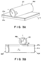
- Figures 3A and 3B are a perspective view and a side view, respectively, for illustrating a rubbing treatment applied to a liquid crystal device according to the invention.
- Figure 4 is a schematic view of a state of a chiral smectic liquid crystal for illustrating C1 alignment and C2 alignment.
- Figures 5A and 5B are schematic views for illustrating liquid crystal alignment states in the vicinity of a substrate boundary in C1 alignment and C2 alignment, respectively.
- Figure 6 is a sectional view for illustrating a structure adopted in an embodiment of the liquid crystal according to the invention.
- Figure 7A is a schematic view of a liquid crystal device for illustrating a manner of evaluating a liquid crystal molecular movement and Figure 7B show two voltage waveforms used therefor, respectively, in an experimental example described hereinafter.
- Figures 8 and 9 are respectively a graph showing a relationship between an average pretilt angle
- the temperature, electric field intensity and electric field frequency have a relationship of trade off with a factor, such as Ps, affecting the response speed and are constrained by design factors, such as frame frequency and duty ratio of a liquid crystal apparatus, such as a display apparatus using the liquid crystal device, so that it is difficult to make a remarkable improvement based on these factors.
- the above-mentioned factors causing a liquid crystal molecular movement in a liquid crystal device are also related with the occurrence of unsatisfactory or incomplete bistability in a device subjected to an asymmetrical aligning treatment.
- the asymmetrical thresholds depend on factors determining the directionality of pretilt angle ⁇ and the smectic layer inclination angle, so that it has been found possible to control these factors based on physical properties of a liquid crystallized, thereby remarkably reducing adverse effects on the bistability.
- At least one substrate is subjected to a uniaxial aligning treatment in normal and reverse two directions in a controlled manner so as to suppress or cancel the tendency or directionality of liquid crystal molecules raising their heads from a substrate, suppress the liquid crystal molecular movement and establish a prescribed relationship among pretilt angle ⁇ , apparent tilt angle ⁇ a, layer inclination angle ⁇ and cone angle H.
- the uniaxial aligning treatment in normal and reverse two directions the directionality of smectic layer inclination or bending is canceled and the occurrence of asymmetrical thresholds is suppressed in a manner of resisting external factors while accomplishing a good alignment state.
- a principal device feature of the present invention is that the boundary surface contacting a liquid crystal of at least one substrate is subjected to a uniaxial aligning treatment in two directions including a normal direction and a reverse direction.
- a uniaxial aligning treatment may preferably be performed by rubbing an insulating layer (alignment control layer) provided on a substrate (electrode plate) or directly the substrate.
- a uniaxial aligning treatment may also be effected by forming a thin film by oblique evaporation or according to the LB (Langmuir-Blodget) method.
- the uniaxial aligning treatment is performed in normal and reverse two directions so as not to weaken the alignment control force but to macroscopically cancel the directionality of the normal and reverse directions, particularly the directionality of pretilt affecting the liquid crystal molecular movement and the asymmetrical thresholds.
- a latter uniaxial aligning treatment e.g., in a reverse direction
- the latter uniaxial aligning treatment should desirably be performed in a weaker intensity (e.g., a weaker rubbing intensity).
- a weaker intensity e.g., a weaker rubbing intensity
- the latter rubbing in the reverse direction is performed in an intensity which is ca. 1/30 to 1/3 times that in the former rubbing in the normal direction. It is possible to repeat the rubbing further several times in alternate directions. Also in such a case, it is preferred to weaken the treatment intensity at least in the last one or two times of treatment sufficiently compared with the treatment intensity in a previous treatment.
- Figures 2A and 2B respectively show a state wherein an insulating film (alignment control layer) 23a formed on a substrate 21a is subjected to a uniaxial aligning treatment as by rubbing in mutually opposite two (i.e., normal and reverse) directions whereby liquid crystal molecules 1 are aligned to be inclined at a prescribed angle (pretilt angle) with respect to the boundary with the alignment control film 23a.
- a uniaxial aligning treatment as by rubbing in mutually opposite two (i.e., normal and reverse) directions whereby liquid crystal molecules 1 are aligned to be inclined at a prescribed angle (pretilt angle) with respect to the boundary with the alignment control film 23a.
- Figure 2A shows a state wherein almost equal numbers of liquid crystal molecules are aligned (inclined) in response to the treatments in the normal and reverse directions so as to provide an absolute value of average pretilt angle
- Figure 2B shows a state wherein the number of liquid crystal molecules inclined in response to a uniaxial aligning treatment in one direction (normal direction in this embodiment) is larger than the number of liquid crystal molecules inclined in response to a uniaxial aligning treatment in the other direction (reverse direction in this embodiment) so as to provide an absolute value of average pretilt angle
- FIGS 3A and 3B are a perspective view and a side view, respectively, showing a manner of rubbing an insulating layer 23a disposed on a substrate 21a.
- a rubbing roller RB1 surfaced with a rubbing cloth 20 and is rotated about its axis in an arbitrary direction (denoted by n ) while applying a pressing force onto the substrate 21a depending on a pressing depth M ( Figure 3B), and the substrate 21a is fed in a desired direction and at a desired speed (denoted by V).
- a reciprocal rubbing i.e., rubbing in normal and reverse two directions
- This alternate feeding i.e., rubbing in alternate directions
- the reciprocal rubbing can be effected without using a roller but by rubbing (the alignment control film 23a on) the substrate 21a with a rubbing cloth while adjusting the pressing depth M and the substrate feed rate V.
- Another characteristic feature of the present invention is that a specific alignment state characterized by several parameters is developed by appropriate selection of device structure inclusive of an alignment film material and a liquid crystal material.
- the uniform alignment state is characterized by a relationship of H ⁇ /2 ⁇ ⁇ a ⁇ H ⁇ representing a switching condition determined by a liquid crystal material and an alignment state, wherein ⁇ a represents an apparent tilt angle which is a half of an angle between the two bistable states, and H represents a tilt angle (cone angle) H which is a half of cone apex angle of a chiral smectic liquid crystal forming in a bulk helical state, i.e., a physical property of the chiral smectic liquid crystal.
- a chiral smectic liquid crystal in the uniform alignment state can assume C1 alignment (state) and/or C2 alignment (state) as shown in Figure 4 and Figures 5A and 5B.
- a chiral smectic liquid crystal generally has a (smectic) layer structure including a plurality of (smectic) layers each composed of plural molecules, and the smectic layer thickness (generally called “layer spacing") may shrink when it is cooled to cause a phase transition from SmA (smectic A) phase to SmC (smectic C) phase or SmC* (chiral smectic C) phase, thereby forming a structure (so-called "chevron structure") wherein the smectic layers 210 are bent at a mid point between the substrates 21a and 21b as shown in Figure 4, while the above tendency can depend on a liquid crystal material used.
- liquid crystal molecular directors 330 in the vicinity of C1 alignment and C2 alignment are present on cones 310 shown in Figures 5A and 5B, respectively.
- a liquid crystal molecule at a substrate boundary forms a pretilt angle ⁇ (angle between a substrate 200 and a liquid crystal molecule 330) so that it raises its head in the direction of rubbing (i.e., the direction of uniaxial alignment treatment A shown in Figures 4, 5A and 5B).
- the device conditions are set so as to allow both of the C1 alignment and C2 alignment, reduce the average inclination angle of smectic layers due to co-presence of C1 and C2 alignments and provide a substantially defect-free, homogeneous alignment state.
- the parameters H, ⁇ and ⁇ are set to satisfy: H ⁇ > ⁇ + ⁇ so as to also allow C2 alignment. It is further preferred to satisfy H ⁇ /2 > ⁇ + ⁇ in order to stably form a uniform alignment state.
- the occurrence of particularly problematic defects as described above has not been observed.
- an increase of zigzag defects in a minute region, such as a pixel can be observed, e.g., as ⁇ or ⁇ increases.
- the occurrence of defects in the present invention may be effected according to the following mechanism. That is, the entire region of liquid crystal is composed of domains having mutually different pretilt angles and layer structures, and the growth of each domain is suppressed so that every domain is suppressed to be a minute one.
- the liquid crystal molecular movement directionality and the directionality of monostabilization (i.e., asymmetrical thresholds) of the individual domains are canceled with each other.
- the liquid crystal layer may preferably assume substantially a bookshelf structure.
- the liquid crystal alignment defects can be reduced to provide a higher brightness and a higher contrast.
- the pretilt angle ⁇ represents an average pretilt angle ⁇ av attained by the above-mentioned aligning treatment in normal and reverse directions, if the condition of H ⁇ > ⁇ + ⁇ is satisfied.
- the above-mentioned device conditions regarding the liquid crystal alignment state may be realized by other device factors, such as a liquid crystal material, a material for the alignment control layers and a relationship between aligning treatments applied to the pair of substrates.
- the liquid crystal material used in the present invention may be a chiral smectic liquid crystal material, i.e., a liquid crystal material having a chiral smectic phase inclusive of chiral smectic C phase (SmC*) as a representative and also chiral smectic H phase (SmH*), I phase (SmI*), K phase (SmK*) and G phase (SmG*) which may be also represented by SmC* in some cases.
- SmC* chiral smectic liquid crystal material
- the liquid crystal material may for example comprise a composition including, as a principal constituent, a mesomorphic compound having a biphenyl skeleton or a phenylpyrimidine skeleton as a mesogen group and various hydrocarbon groups optionally substituted with a halogen as side or terminal chains, and also at least one species of chiral dopant.
- liquid crystal material suitable for developing the above-mentioned bookshelf structure it is preferred to use a liquid crystal material showing a small layer inclination angle ⁇ and a large cone angle H.
- a liquid crystal material may include those showing no or only suppressed cholesteric (Ch) phase.
- Such a liquid crystal material may for example include a mesomorphic compound having a mesogen group comprising a ring structure, such as a naphthalene skeleton or a phenylpyrimidine skeleton, and a fluorocarbon chain group.
- More specific examples thereof may include chiral mesomorphic compounds having a ring structured skeleton of phenylpyrimidine, phenylbenzoate, biphenyl, naphthalene, etc., and also a fluoroalkyl chain group, particularly a terminal perfluoroalkyl group as disclosed in U.S. Patent No. 4,886,619; and achiral mesomorphic compounds having a ring-structured skeleton and a fluoroalkyl chain group, particularly a terminal perfluoroalkyl group.
- the alignment control layer formed on a substrate in the liquid crystal device according to the present invention may comprise a film of an organic polymer, such as polyimide, polyamide, polyvinyl alcohol, or polyester, or a film of an inorganic material, such as silicon oxide, or silicon nitride. It is particularly preferred to use a material such as a polyimide (e.g., "LP-64" available from Toray K.K.) or a polyamide, having a tendency of providing a low pretilt angle.
- an organic polymer such as polyimide, polyamide, polyvinyl alcohol, or polyester
- an inorganic material such as silicon oxide, or silicon nitride.
- a material such as a polyimide (e.g., "LP-64" available from Toray K.K.) or a polyamide, having a tendency of providing a low pretilt angle.
- Figure 6 shows a structure adopted in an embodiment of the liquid crystal device according to the present invention.
- the liquid crystal device includes a pair of substrates 21a and 21b having successively thereon transparent electrodes 22a or 22b and an alignment control layer 23a or 23b, and a chiral smectic liquid crystal 25 and spacer beads 24 disposed between the substrates.
- At least one of the substrates 21a and 21b should be transparent and may for example comprise glass (as a preferred example), a polymer, quartz, metal such as Si or Al, a semiconductor or an insulating material.
- the transparent electrodes 22a and 22b may for example comprise tin oxide, indium oxide, or indium tin oxide (ITO).
- the spacer 24 may comprise fine particles of, e.g., alumina or silica.
- a periphery of the pair of substrates may be sealed with a sealing member (not shown) of, e.g., an epoxy resin to provide a cell structure, which is filled with the liquid crystal 25.
- the thus-formed liquid crystal cell structure is sandwiched between a pair of polarizers 26a and 26b.
- a backlight (not shown) may be further provided outside one of the polarizers 26a and 26b in order to provide a transmission-mode device.
- a pair of the substrates 21a and 21b may be provided with an asymmetrical aligning treatment such that only one of the substrates 21a an 21b is subjected to a uniaxial aligning treatment in normal and reverse two directions and the other is provided with a non-uniaxial aligning surface, e.g., by having an alignment control film of a material identical to or different from that of the opposite alignment control layer but not subjected to a uniaxial aligning treatment, and a liquid crystal material not showing cholesteric phase may be disposed between the substrates, thereby forming a homogeneous, defect-free alignment state.
- a sample cell was prepared by applying a pair of substrates each other so that the inclination of liquid crystal at the boundaries with two substrates were parallel and identical to each other, and the cell was then filled with a liquid crystal mixture assuming SmA phase in the temperature range of 10 - 55 °C obtained by mixing 80 wt. % of a ferroelectric liquid crystal ("CS-1014", mfd. by Chisso K.K.) with 20 wt. % of a compound represented by the following formula:
- the liquid crystal cell was rotated in a plane perpendicular to the pair of substrates and including the aligning treatment axis and, during the rotation, the cell was illuminated with a helium-neon laser beam having a polarization plane forming an angle of 45 degrees with respect to the rotation plane in a direction normal to the rotation plane, whereby the intensity of the transmitted light was measured by a photodiode from the opposite side through a polarizer having a transmission axis parallel to the polarization plane.
- Figure 7A is a schematic plan view of a sample liquid crystal cell and Figure 7B shows signals applied to the sample cell.
- a pair of substrates prepared by a method are applied to each other so that an aligning treatment direction 40 is disposed perpendicular to printed mutually parallel stripe spacers 43, and a gap therebetween is filled with a liquid crystal without sealing on both sides to form a sample cell.
- the silicone oil is pulled into the cell to indicate the degree of the liquid crystal movement.
- the rate of liquid crystal molecular movement was evaluated by the distance of the marker introduced into the cell.
- LP-64 polyimide precursor
- silica beads having an average particle size of 1.5 ⁇ m were dispersed, and the other substrate was superposed thereon so that their normal rubbing directions (and accordingly also the reverse rubbing directions) were parallel and identical to each other to form a cell.
- each cell was filled with a mixture liquid crystal A showing a phase transition series of Cry ⁇ SmC* ⁇ SmA ⁇ Iso. on temperature increase, a tilt angle (cone angle) H of at least 25 degrees, an apparent tilt angle ⁇ a of at least 20 degrees, a spontaneous polarization (Ps) of 20 ⁇ C/cm2 and a smectic layer inclination angle ⁇ of 6.5 degrees, respectively, in chiral smectic phase at 30 °C.
- the filling was performed with the mixture liquid crystal A in isotropic phase, and the resultant cell was gradually cooled at a rate of 0.5 °C/min to room temperature to effect alignment.
- the liquid crystal molecular movement speed can be suppressed and the effect is remarkable when the pretilt angle
- Example 2 Twelve pairs of 1.1 mm-thick glass substrates each provided with a ca. 150 nm-thick ITO transparent electrode film were provided similarly as in Example 1.
- silica beads having an average particle size of 1.5 ⁇ m were dispersed, and then other substrate was superposed thereon to form a cell.
- each cell was filled with the same mixture liquid crystal A as used in Example 1 in isotropic phase by injection under vacuum, and then gradually cooled at a rate of 0.5 °C/min to room temperature to effect alignment.
- the liquid crystal molecular movement speed could be suppressed and the effect was remarkable when the pretilt angle
- silica beads having an average diameter of 1.5 ⁇ m were dispersed, and the other substrate was superposed thereon so that their normal rubbing directions (and accordingly also the reverse rubbing directions) were parallel and opposite to each other (i.e., in a so-called anti-parallel arrangement).
- the liquid crystal molecular movement was evaluated in the same manner as in Example 1.
- liquid crystal molecular movement was also effectively suppressed at a pretilt angle
- the liquid crystal device of the present invention is suitable for constituting liquid crystal apparatus, such as a light valve and a display apparatus, in combination with various drive circuits therefor.
- a liquid crystal device is constituted by a pair of substrates, and a chiral smectic liquid crystal assuming at least two stable states disposed between the two substrates. At least one of the substrates is subjected to a uniaxial aligning treatment in two directions including a normal direction and a reverse direction substantially opposite to the normal direction.
- the liquid crystal is placed in an alignment state such that the liquid crystal provides an apparent tilt angle ⁇ a which is a half of an angle between said two stable states, a tilt angle H and a pretilt angle ⁇ with respect to a substrate surface, and forms smectic layers forming an inclination angle ⁇ from a normal to the substrate surfaces, satisfying: H ⁇ /2 ⁇ ⁇ a ⁇ H ⁇ and H ⁇ > ⁇ + ⁇ .
- an undesirable liquid crystal molecular movement along the substrates is effectively suppressed.
Landscapes
- Physics & Mathematics (AREA)
- Nonlinear Science (AREA)
- Chemical & Material Sciences (AREA)
- Crystallography & Structural Chemistry (AREA)
- General Physics & Mathematics (AREA)
- Optics & Photonics (AREA)
- Spectroscopy & Molecular Physics (AREA)
- Mathematical Physics (AREA)
- Liquid Crystal (AREA)
Applications Claiming Priority (4)
| Application Number | Priority Date | Filing Date | Title |
|---|---|---|---|
| JP253053/93 | 1993-10-08 | ||
| JP25305393 | 1993-10-08 | ||
| JP89943/94 | 1994-04-27 | ||
| JP6089943A JP2952150B2 (ja) | 1993-10-08 | 1994-04-27 | 液晶素子及びその製造方法 |
Publications (2)
| Publication Number | Publication Date |
|---|---|
| EP0647873A2 true EP0647873A2 (de) | 1995-04-12 |
| EP0647873A3 EP0647873A3 (de) | 1995-11-02 |
Family
ID=26431328
Family Applications (1)
| Application Number | Title | Priority Date | Filing Date |
|---|---|---|---|
| EP94115842A Withdrawn EP0647873A3 (de) | 1993-10-08 | 1994-10-07 | Flüssigkristallvorrichtung. |
Country Status (7)
| Country | Link |
|---|---|
| US (1) | US5568295A (de) |
| EP (1) | EP0647873A3 (de) |
| JP (1) | JP2952150B2 (de) |
| KR (1) | KR0159969B1 (de) |
| CN (1) | CN1064138C (de) |
| AU (1) | AU673459B2 (de) |
| CA (1) | CA2133711C (de) |
Families Citing this family (10)
| Publication number | Priority date | Publication date | Assignee | Title |
|---|---|---|---|---|
| US5726725A (en) * | 1994-03-31 | 1998-03-10 | Canon Kabushiki Kaisha | Liquid crystal device and process for production thereof with polyimide alignment film rubbed and then baked |
| US5798056A (en) * | 1995-02-01 | 1998-08-25 | Canon Kabushiki Kaisha | Aligning method of liquid crystal, production process of liquid crystal device, and liquid crystal device |
| US6151090A (en) * | 1995-05-31 | 2000-11-21 | Casio Computer Co., Ltd. | LCD using liquid crystal of ferroelectric and/or antiferroelectric phase having pretilt angle of 1 degree or less |
| US5932136A (en) * | 1995-10-20 | 1999-08-03 | Canon Kabushiki Kaisha | Liquid crystal device and liquid crystal apparatus |
| JP3192593B2 (ja) * | 1996-07-22 | 2001-07-30 | キヤノン株式会社 | 液晶素子 |
| US6019789A (en) | 1998-04-01 | 2000-02-01 | Quanam Medical Corporation | Expandable unit cell and intraluminal stent |
| US20070279541A1 (en) * | 2005-06-29 | 2007-12-06 | Nano Loa, Inc. | Method of driving liquid crystal display device |
| US20070002267A1 (en) * | 2005-06-29 | 2007-01-04 | Nano Loa, Inc. | Liquid crystal display device |
| US20070003709A1 (en) * | 2005-06-29 | 2007-01-04 | Nano Loa, Inc. | Liquid crystal display device |
| US20070229743A1 (en) * | 2006-04-04 | 2007-10-04 | Chein-Wen Chen | Alignment method |
Family Cites Families (11)
| Publication number | Priority date | Publication date | Assignee | Title |
|---|---|---|---|---|
| US4367924A (en) * | 1980-01-08 | 1983-01-11 | Clark Noel A | Chiral smectic C or H liquid crystal electro-optical device |
| US4886619A (en) * | 1986-06-30 | 1989-12-12 | Minnesota Mining And Manufacturing Company | Fluorine-containing chiral smectic liquid crystals |
| JP2568574B2 (ja) * | 1987-08-26 | 1997-01-08 | 松下電器産業株式会社 | 液晶セルの製造方法 |
| JP2568575B2 (ja) * | 1987-08-26 | 1997-01-08 | 松下電器産業株式会社 | 液晶セルの製造方法 |
| US5172255A (en) * | 1989-10-06 | 1992-12-15 | Nokia Unterhaltungselektronik (Deutschland) Gmbh | Process for increasing pretilt angles in nematic liquid crystal cells |
| US5189536A (en) * | 1990-03-02 | 1993-02-23 | Canon Kabushiki Kaisha | Ferroelectric liquid crystal element having uniform high temperature alignment |
| JPH04195119A (ja) * | 1990-11-28 | 1992-07-15 | Fujitsu Ltd | 液晶パネルの製造方法 |
| JP2775528B2 (ja) * | 1991-02-01 | 1998-07-16 | キヤノン株式会社 | カイラルスメクチック液晶素子 |
| JP2952122B2 (ja) * | 1991-11-22 | 1999-09-20 | キヤノン株式会社 | 液晶素子、及びこれを用いた表示装置 |
| JP3100014B2 (ja) * | 1991-12-10 | 2000-10-16 | キヤノン株式会社 | 強誘電性液晶素子及び該素子の製造方法 |
| CA2121776C (en) * | 1993-04-28 | 1999-05-25 | Yasuto Kodera | Liquid crystal device with a liquid crystal in an optical modulation region having a pretilt angle smaller than the liquid crystal in a peripheral region surrounding the optical modulation region |
-
1994
- 1994-04-27 JP JP6089943A patent/JP2952150B2/ja not_active Expired - Fee Related
- 1994-10-05 CA CA002133711A patent/CA2133711C/en not_active Expired - Fee Related
- 1994-10-05 US US08/318,432 patent/US5568295A/en not_active Expired - Fee Related
- 1994-10-07 AU AU74490/94A patent/AU673459B2/en not_active Ceased
- 1994-10-07 EP EP94115842A patent/EP0647873A3/de not_active Withdrawn
- 1994-10-08 CN CN94112833.4A patent/CN1064138C/zh not_active Expired - Fee Related
- 1994-10-08 KR KR1019940025788A patent/KR0159969B1/ko not_active Expired - Fee Related
Also Published As
| Publication number | Publication date |
|---|---|
| CN1064138C (zh) | 2001-04-04 |
| CN1109980A (zh) | 1995-10-11 |
| AU673459B2 (en) | 1996-11-07 |
| CA2133711C (en) | 1999-09-14 |
| KR0159969B1 (ko) | 1999-01-15 |
| JPH07152036A (ja) | 1995-06-16 |
| JP2952150B2 (ja) | 1999-09-20 |
| AU7449094A (en) | 1995-05-11 |
| EP0647873A3 (de) | 1995-11-02 |
| US5568295A (en) | 1996-10-22 |
| CA2133711A1 (en) | 1995-04-09 |
Similar Documents
| Publication | Publication Date | Title |
|---|---|---|
| EP0550846B1 (de) | Ferroelektrische Flüssigkristall-Anzeigevorrichtung und Verfahren zu ihrer Herstellung | |
| EP0553727B1 (de) | Verfahren zur Behandlung einer chiralen smektischen Flüssigkristallvorrichtung | |
| KR0125785B1 (ko) | 액정 소자 | |
| EP0683417A1 (de) | Flüssigkristallelement und Flüstigkristallgerät | |
| US6310677B1 (en) | Liquid crystal device and liquid crystal display apparatus having a chevron structure in monostable alignment | |
| JP2612503B2 (ja) | 液晶素子 | |
| EP0539992A1 (de) | Flüssigkristall-Anzeigevorrichtung | |
| US5353141A (en) | Method for aligning treatment of liquid crystal device including varying with time the feeding speed of the rubbing roller | |
| US5568295A (en) | Chiral smetic LCD with small pretilt angle, substrate rubbed in two opposing directions, and no cholesteric phase or tilt angle > the pretilt plus inclination angles | |
| US5668615A (en) | LCD device with alignment films having a pretilt changing characteristic | |
| US5999157A (en) | Suppressing liquid crystal movement based on the relationship between a display pattern and a driving waveform | |
| US5798056A (en) | Aligning method of liquid crystal, production process of liquid crystal device, and liquid crystal device | |
| US5956010A (en) | Liquid crystal apparatus and driving method | |
| US5668616A (en) | Ferroelectric liquid crystal device with alignment layers having surface unevenness different from each other | |
| US6551669B2 (en) | Monostable ferroelectric liquid crystal display apparatus | |
| US5726725A (en) | Liquid crystal device and process for production thereof with polyimide alignment film rubbed and then baked | |
| JPH07181522A (ja) | 液晶表示装置 | |
| JP2983724B2 (ja) | 強誘電性液晶素子の配向処理法 | |
| KR100802306B1 (ko) | 액정 표시 장치 및 그 제조방법 | |
| JP3180171B2 (ja) | 強誘電性液晶素子 | |
| US5844653A (en) | Liquid crystal mixture | |
| EP0271344B1 (de) | Flüssigkristallanzeigeelement und Verfahren zu dessen Betrieb | |
| JPH07181495A (ja) | 強誘電性液晶素子 | |
| JPH07325304A (ja) | 液晶表示素子 | |
| JPH05341289A (ja) | 液晶表示装置 |
Legal Events
| Date | Code | Title | Description |
|---|---|---|---|
| PUAI | Public reference made under article 153(3) epc to a published international application that has entered the european phase |
Free format text: ORIGINAL CODE: 0009012 |
|
| 17P | Request for examination filed |
Effective date: 19941007 |
|
| AK | Designated contracting states |
Kind code of ref document: A2 Designated state(s): AT BE CH DE DK ES FR GB GR IE IT LI LU MC NL PT SE |
|
| PUAL | Search report despatched |
Free format text: ORIGINAL CODE: 0009013 |
|
| AK | Designated contracting states |
Kind code of ref document: A3 Designated state(s): AT BE CH DE DK ES FR GB GR IE IT LI LU MC NL PT SE |
|
| 17Q | First examination report despatched |
Effective date: 19980109 |
|
| STAA | Information on the status of an ep patent application or granted ep patent |
Free format text: STATUS: THE APPLICATION IS DEEMED TO BE WITHDRAWN |
|
| 18D | Application deemed to be withdrawn |
Effective date: 20010725 |