EP0649037B1 - Dispositif optique de diffraction - Google Patents
Dispositif optique de diffraction Download PDFInfo
- Publication number
- EP0649037B1 EP0649037B1 EP94116398A EP94116398A EP0649037B1 EP 0649037 B1 EP0649037 B1 EP 0649037B1 EP 94116398 A EP94116398 A EP 94116398A EP 94116398 A EP94116398 A EP 94116398A EP 0649037 B1 EP0649037 B1 EP 0649037B1
- Authority
- EP
- European Patent Office
- Prior art keywords
- grating
- diffractive optical
- optical device
- period
- light
- Prior art date
- Legal status (The legal status is an assumption and is not a legal conclusion. Google has not performed a legal analysis and makes no representation as to the accuracy of the status listed.)
- Expired - Lifetime
Links
Images


Classifications
-
- G—PHYSICS
- G02—OPTICS
- G02B—OPTICAL ELEMENTS, SYSTEMS OR APPARATUS
- G02B5/00—Optical elements other than lenses
- G02B5/18—Diffraction gratings
- G02B5/1876—Diffractive Fresnel lenses; Zone plates; Kinoforms
-
- G—PHYSICS
- G02—OPTICS
- G02B—OPTICAL ELEMENTS, SYSTEMS OR APPARATUS
- G02B6/00—Light guides; Structural details of arrangements comprising light guides and other optical elements, e.g. couplings
- G02B6/10—Light guides; Structural details of arrangements comprising light guides and other optical elements, e.g. couplings of the optical waveguide type
- G02B6/12—Light guides; Structural details of arrangements comprising light guides and other optical elements, e.g. couplings of the optical waveguide type of the integrated circuit kind
- G02B6/122—Basic optical elements, e.g. light-guiding paths
- G02B6/124—Geodesic lenses or integrated gratings
Definitions
- the present invention relates to a diffractive optical device, especially a diffractive optical device preventing reduction in the diffraction efficiency even in an area having a small grating period.
- a diffractive optical device which utilizes diffraction of light, has a grating pattern for diffraction.
- the grating pattern is formed by arranging a plurality of grating elements on a substrate.
- the diffraction efficiency which is the ratio of light which can be diffracted with respect to the light incident on the diffractive optical device, is determined by the grating pattern. Generally, how high the diffraction efficiency can be is a matter of a prime importance in determining the quality of the diffractive optical device.
- FIG. 1 is a plan view of the microlens 100 illustrating a grating pattern thereof
- Figure 2 is a cross sectional view of the microlens 100
- the microlens 100 includes a substrate 11 . Light which is incident vertically on a bottom surface of the substrate 11 is collected or collimated above the substrate 11 . As is shown in Figure 1 , a plurality of grating elements 18 are arranged concentrically on a top surface of the substrate 11 to form a grating pattern.
- each grating element 18 has a rectangular cross section.
- FIG 3 is a cross sectional view of another diffractive microlens 200 proposed by J. Jahns and S. J. Walker in "Two-dimensional array of diffractive microlenses fabricated by thin film deposition", Applied Optics Vol. 29, No. 7, pp. 931-936 (1990).
- the microlens 200 includes a substrate 11 and a plurality of grating elements 28 arranged on a top surface of the substrate 11 .
- Each grating element 28 has multiple discrete phase levels.
- each grating element 28 has four phase levels including the top surface of the substrate 11 .
- Adopting such a way of counting each grating element 18 in the microlens 100 in Figure 2 has two phase levels. This way of counting the phase levels of the grating elements will be used throughout this specification.
- the diffractive microlens 100 has a diffraction efficiency of 41%
- the microlens 200 has a diffraction efficiency of as high as 81%. It has been found that the larger the number of phase levels of the grating element is, the higher the diffraction efficiency is. For example, the diffraction efficiency is 95% where each grating element has eight phase levels, and the diffraction efficiency is 99% where each grating element has 16 phase levels.
- the researchers including the inventors of the present invention have found that the diffraction efficiency is significantly reduced as the number of the phase levels is increased in an area where the grating period is relatively small, namely, proximate to the wavelength of the incident light.
- This diffractive optical element comprises a base and first and second phase zones, the first phase zone comprising a first multiplicity of steps and the second phase zone comprising a second multiplicity of steps, wherein the first multiplicity and the second multiplicity of steps are different. It is, however, not disclosed in this document how to optimize a diffraction efficiency in the entire area of the diffractive optical device, when light is incident at an offset angle with respect to the vertical direction of a disposition plane of the multiplicity of the grating elements.
- One aspect of the present invention relates to a diffractive optical device including a substrate for allowing transmission therethrough of light to be diffracted; and a grating section located on the substrate and including a plurality of grating elements each having multiple discrete phase levels.
- the plurality of grating elements are arranged at different grating periods in different areas of a surface of the substrate and have the phase levels in different numbers in accordance with the grating period.
- the number of the phase levels becomes progressively smaller in accordance with decrease in the grating period.
- the number of the phase levels is at least 3 in an area where the grating period is at least a first value obtained by multiplying a wavelength of the light by a first prescribed number.
- the number of the phase levels is 2 in an area where the grating period is less than the first value.
- the first prescribed number is substantially between 1.5 and 3.
- the grating section has a duty ratio of substantially between 0.15 and 0.5 in the area where the grating period is less than the first value.
- the number of the phase levels is at least 4 in an area where the grating period is at least a second value obtained by multiplying the wavelength of the light by a second prescribed number.
- the number of the phase levels is 3 in an area where the grating period is smaller than the second value and at least the first value.
- the second value is substantially between 2 and 5 and greater than the first prescribed number.
- the number of the phase levels is at least 5 in an area where the grating period is at least a third value obtained by multiplying the wavelength of the light by a third prescribed number.
- the number of the phase levels is 4 in an area where the grating period is smaller than the third value and at least the second value.
- the third value is substantially between 4 and 7 and greater than the second prescribed number.
- the grating elements have different heights in accordance with the number of the phase levels thereof.
- the bottommost level among the multiple discrete phase levels is the surface of the substrate.
- the smallest grating period is greater than 1/2n of the wavelength of the light where n is the refractive index of the substrate, and the duty ratio of the grating section changes in accordance with the grating period.
- the grating elements are symmetrically arranged with respect to the center thereof and are arcked in an identical direction, and the grating period becomes progressively smaller in the direction.
- the plurality of grating elements are extended in straight lines in an identical direction, and the grating period changes in a direction which is perpendicular to the direction in which the grating elements are extended.
- the grating section is covered with a thin film.
- the thin film is reflective.
- the thin film is non-reflective.
- the substrate includes a light guide region for propagating the light.
- a diffractive optical device including a substrate for allowing transmission therethrough of light to be diffracted; and a grating section located on the substrate and including a plurality of grating elements.
- the plurality of grating elements are arranged at different grating periods in different areas of a surface of the substrate.
- the smallest grating period is greater than 1/2n of the wavelength of the light where n is the refractive index of the substrate.
- the grating section has a duty ratio changing in accordance with the grating period.
- the duty ratio is less than 0.5 in an area where the grating period is less than three to four times the wavelength of the light.
- the duty ratio becomes progressively smaller in accordance with decrease in the grating period.
- the plurality of grating elements have different heights in accordance with the grating period.
- the height of the plurality of grating elements becomes progressively smaller in accordance with decrease in the grating period in an area where the grating period is less than three to four times the wavelength of the light.
- a part of the plurality of grating elements each have at least three discrete phase levels.
- the invention described herein makes possible the advantages of providing a diffractive optical device which has a high diffraction efficiency in the entire area thereof for the light which is incident thereon at an angle offset with respect to the vertical direction thereto and which has grating elements easily fabricated even with a small grating period.
- Figure 4 is a cross sectional view of the diffractive optical device 10
- Figure 5 is a plan view thereof.
- the diffractive optical device 10 includes a substrate 1 and a grating section 2 located on a top surface of the substrate 1 .
- the substrate 1 and the grating section 2 are formed of a material which allows transmission therethrough of light of at least a wavelength to be diffracted (for example, light having a wavelength of 0.6328 ⁇ m).
- the substrate 1 and the grating section 2 may be formed of different materials from each other or may be integrally formed of an identical material.
- the grating section 2 includes a plurality of grating elements 21 arranged so as to form a grating pattern.
- Each grating element 21 has a cross section having a plurality of steps, namely, has has multiple phase levels.
- the diffractive optical device 10 is used, for example, as an off-axis lens as is shown in Figure 6 .
- An axis of light incident on an off-axis lens is different from an axis of light outgoing from the off-axis lens.
- light 5 which is propagated zigzag in a light guide region 12 in the substrate 1 goes out through the top surface of the substrate 1 as outgoing light 6 .
- the light guide region 12 is provided with reflective layers 4A and 4B respectively on a top surface and a bottom surface thereof for reflecting the light 5 alternately in repetition.
- the light 5 is propagated zigzag from the negative side to the positive side of axis y and is incident on the grating section 2 at an incident angle of which is offset with respect to the vertical direction to the top surface of the substrate 1 . Then, the light 5 is transmitted through the grating section 2 and goes out to above the substrate 1 vertically.
- “goes out vertically” means that the axis of the outgoing light 6 is substantially vertical to the top surface of the substrate 1 , namely, parallel to axis z.
- the grating section 2 has a grating pattern as shown in Figure 5 in order to collect the light 5 incident at an offset angle at point 3 which is away from the top surface of the substrate 1 by distance f.
- Each grating element 21 forming the grating pattern is arcked while projecting toward the positive direction of axis y.
- the grating period is progressively reduced and the curvature of the grating elements 21 is progressively increased toward the positive direction of axis y.
- an optical data recording medium such as an optical disc may be placed.
- at least a part of the outgoing light 6 is reflected by the optical data recording medium and thus returns to the diffractive optical device 10 .
- the light reflected by the optical data recording medium is guided to a light detector.
- the diffractive optical device 10 can be used for various other uses.
- one substrate may be commonly used for a plurality of diffractive optical devices by providing a plurality of grating sections 2 on the top surface, on a bottom surface, or on both of the top and the bottom surfaces of the substrate 1 .
- Other types of optical devices utilizing no diffraction effect such as a laser light source or a light detector may also be provided on the substrate 1 .
- each grating element 21 in area 2B has three phase levels while each grating element 21 in area 2A has two phase levels.
- each grating element 21 in area 2B includes a first level having a height of 0 from the top surface of the substrate 1 , a second level having a height of 1/2 h B , and a third level having a height of h B .
- Each grating element 21 in area 2A includes a first level having a height of 0 from the top surface of the substrate 1 and a second level having a height of h A .
- the diffraction efficiency at three phase levels was higher than that at two phase levels in area 2B having a relatively large grating period.
- area 2A having a grating period proximate to the wavelength of the incident light the diffraction efficiency at three phase levels was rapidly reduced; and the diffraction efficiency at two phase levels was reduced at a smaller ratio or even raised.
- Figure 7 is a graph illustrating the relationship between the normalized grating period ⁇ / ⁇ and the diffraction efficiency.
- Symbol ⁇ denotes the grating period
- symbol ⁇ denotes the wavelength of the light.
- the experiment was performed under the conditions that the incident angle ⁇ of the light was 20° and the refractive index n of areas 2A and 2B was 1.5.
- the solid line in Figure 7 in the case of the grating elements each having three phase levels, the diffraction efficiency is more than 50% in area 2B having a relatively large grating period but is reduced drastically in area 2A where the grating period is proximate to the wavelength of the incident light.
- the diffraction efficiency is 30 to 40% in area 2B but increases as the grating period decreases. Especially from the point at which the grating period is approximately twice or three times the wavelength of the incident light, the diffraction efficiency rapidly increases as the grating period decreases. For example, where the grating period is 1.6 times the wavelength of the incident light, the diffraction efficiency of the grating elements having two phase levels is equal to the diffraction efficiency of the grating elements having three phase levels.
- the diffraction efficiency can be high in the entire diffractive optical device 10 .
- the grating elements having three phase levels can be properly produced in an area where the grating period is relatively large, but the grating elements having three phase levels cannot be produced so as to have sharp-edged steps in an area where the grating period is relatively small.
- the diffractive optical device 10 in this example only two phase levels are sufficient for the grating elements 21 in an area where the grating period is less than 1.6 times the wavelength of the incident light.
- precision processing is easier and the grating elements 21 can be produced as designed.
- the number of phase levels is changed from two to three at the normalized grating period of 1.6 (namely, when the grating period is 1.6 times the wavelength of the incident light).
- the optimum normalized grating period at which the number of phase levels should be changed is different depending on the incident angle of light and the like, it has been confirmed that substantially the same effects are obtained as long as the number of phase levels is changed at the normalized grating period of between 1.5 and 3.
- the other parameters of the diffractive optical device 10 in this example are, for example, as follows:
- the diameter of a circular opening is 1 mm;
- the wavelength of the incident light ⁇ is 0.6328 ⁇ m;
- the incident angle of light ⁇ 20°;
- the focal distance is 2.5 mm.
- the grating period is, for example, between 1.0 and 2.0 ⁇ m; and the height h B is, for example, 0.84 ⁇ m.
- the grating period is, for example, between 0.89 ⁇ m and 1.0 ⁇ m; and the height h A is, for example, 0.63 ⁇ m.
- the height of the grating element 21 is changed in accordance with the number of phase levels, in which manner the diffraction efficiency is optimized.
- the duty ratio d1/ ⁇ A ( Figure 4 ) is, for example, 0.3.
- the duty ratio is the ratio of an area occupied by a material other than air with respect to the total area of one grating period in terms of the cross section of the grating section 2 .
- the grating pattern shown in Figure 5 will be described in detail.
- the grating pattern of a diffractive optical device according to the present invention is not limited to the one shown in Figure 5 , but can be arbitrarily designed in accordance with the use.
- the substrate 1 and the grating section 2 which allow transmission therethrough of light to be diffracted are formed of, for example, glass or a synthetic resin.
- the substrate 1 and the grating section 2 may be formed of a semiconductor material such as Si or GaAs.
- the diffractive optical device 10 in the first example is produced by an electron beam drawing method.
- the substrate 1 is coated with a synthetic resin such as an electron beam resist (for example, PMMA or CMS) which is sensitive to an electron beam, and an electron beam is radiated to the layer of the synthetic resin.
- the amount of the electron beam to be radiated is controlled. For example, when a positive resist is used, the electron beam is radiated in a smaller amount to an area which is relatively thick so as to increase the ratio of the thickness remaining after the development with respect to the thickness before development.
- the resultant laminate is developed to produce the diffractive optical device 10 .
- a diffractive optical device according to the present invention may be produced with any other specifications suitable for the use.
- the diffractive optical devices may be produced at a lower cost by forming a mold by a nickel electroforming method and duplicating the mold using a UV curable resin. Especially diffractive optical devices arranged in an array can be produced at a high precision with uniform characteristics at one time in this manner.
- the grating section 2 formed of a synthetic resin such an electron beam resist may be transferred onto the substrate 1 formed of glass or the like by ion beam etching. In such a case, the diffractive optical device is stable in performance against temperature change.
- the diffraction efficiency does not necessarily increase as the numbers of phase levels increases in the entire area of the grating section 2 .
- the diffraction efficiency has a peak at different number of phase levels in accordance with the grating period. Accordingly, by setting the number of phase levels of the grating elements to be optimum in accordance with the grating period, the diffraction efficiency can be high in the entire diffractive optical device 10 . Moreover, since the optimum number of phase levels tends to decrease as the grating period decreases in an area where the grating period is relatively small, even the grating elements having a small grating period can be easily fabricated.
- FIG 8 is a plan view of the diffractive optical device 20 .
- Identical elements with those in the first example will bear identical reference numerals therewith, and explanation thereof will be omitted.
- grating elements 22 in the grating section 2 provided on the substrate 1 are straight lines in shape extending in the direction of axis x.
- the grating period changes in the direction of axis y.
- the diffractive optical device 20 having such grating elements 22 is used as a cylindrical off-axis lens for collecting light incident at an offset angle with respect to the vertical direction to the surface of the substrate 1 only in the direction of one axis. In the example shown in Figure 8 , the light is collected in the direction of axis y.
- the diffractive optical device 20 has a similar cross sectional view as that of the diffractive optical device 10 shown in Figure 4 .
- the same effects as obtained in the first example can be obtained by providing the grating elements 22 having three phase levels in area 2B' where the grating period is relatively large and providing the grating elements 22 having two phase levels in area 2A' where the grating period is relatively small.
- Figure 9 is a cross sectional view illustrating a basic structure of the diffractive optical device 30 .
- Figure 10 is a graph illustrating the relationship between the normalized grating period and the efficiency of first order diffraction when the incident angle of light is 20°.
- Figure 11 is a graph illustrating the relationship between the normalized grating period and the efficiency of first order diffraction when the incident angle of light is 30°. Identical elements with those in the first example will bear identical reference numerals therewith, and explanation thereof will be omitted.
- the diffractive optical device 30 is an off-axis lens in which the grating period changes toward one direction.
- the grating section 2 including grating elements 23 are divided into four areas 2A" through 2D" . In area 2D" where the grating period is largest among in the four areas, each grating element 23 has five phase levels.
- the grating elements 23 each have four phase levels in area 2C" where the grating period is second largest, three phase levels in area 2B" where the grating period is second smallest, and two phase levels in area 2A" where the grating period is smallest among in the four areas.
- area 2A has a normalized grating period of, for example, 1.2 ⁇ ⁇ / ⁇ ⁇ 1.6.
- Area 2B has a normalized grating period of, for example, 1.6 ⁇ ⁇ / ⁇ ⁇ 3.1.
- Area 2C has a normalized grating period of, for example, 3.1 ⁇ ⁇ / ⁇ ⁇ 4.7.
- Area 2D has a normalized grating period of, for example, 4.7 ⁇ ⁇ / ⁇ ⁇ 5.5.
- the height of each area is, for example, 0.633 ⁇ m in area 2A ", 0.84 ⁇ m in area 2B “, 0.95 ⁇ m in area 2C ", and 1.01 ⁇ m in area 2D" .
- the other parameters of the diffractive optical device 30 are, for example, as follows:
- the focal distance is 1.4 mm, which is shorter than that of the off-axis lens 10 in the first example. In an off-axis lens having such a short focal distance, the grating period changes at a higher ratio.
- the diffraction efficiency of the grating elements having five phase levels becomes lower than the diffraction efficiency of the grating elements having four phase levels at the normalized grating period of 4.7.
- the diffraction efficiency of the grating elements having four phase levels becomes lower than the diffraction efficiency of the grating elements having three phase levels at the normalized grating period of 3.1.
- the diffraction efficiency of the grating elements having three phase levels becomes lower than the diffraction efficiency of the grating elements having two phase levels at the normalized grating period of 1.6. Accordingly, by providing the grating elements 23 having the optimum phase levels for each area, the diffraction efficiency can be high in the entire diffractive optical device 30 .
- Figure 11 shows the relationship between the normalized grating period and the efficiency of first order diffraction when the incident angle of light is 30°.
- the optimum normalized grating period at which the number of phase levels should be changed is also changed. Nonetheless, the inventors of the present invention have confirmed that the same effects are obtained as long as the number of phase levels is changed from five to four at the normalized grating period of between 4 and 7, from four to three at the normalized grating period of between 2 and 5, and from three to two at the normalized grating period of between 1.5 and 3.
- an off-axis lens for collecting light incident at an offset angle vertically is described.
- the present invention provides the same effects in other types of diffractive optical devices in the case that the light is incident at an offset angle.
- FIG. 12 is a cross sectional view of the diffractive optical device 40
- Figure 13 is a plan view thereof. Identical elements with those in the first example will bear identical reference numerals therewith, and explanation thereof will be omitted.
- the diffractive optical device 40 has a similar plan view with that of the diffractive optical device 10 in Figure 5 but has a different cross sectional view from that of the diffractive optical device 10 .
- Grating elements 24 in the grating section 2 each have a rectangular cross sectional view.
- the duty ratio d/ ⁇ changes in accordance with the grating period. Symbol ⁇ denotes the grating period, and symbol ⁇ denotes the wavelength of the light.
- the duty ratio is the ratio of an area occupied by a material other than air with respect to the total area of one grating period in terms of the cross section of the grating section 2 .
- each grating period ⁇ is set to be larger than ⁇ /2.
- each grating period ⁇ is set to be larger than ⁇ /2n.
- the duty ratio is set for 0.5 in an area where the grating period is relatively large and to be reduced in correspondence with decrease in the grating period. (The duty ratio will be described in detail later.)
- the height h of the grating elements 24 is constant regardless of the grating period.
- the grating period is, for example, 0.633 ⁇ m to 6.3 ⁇ m, and the height h of the grating elements 24 is, for example, 0.63 ⁇ m.
- the diffraction efficiency was highest at the duty ratio of approximately 0.5 in an area having a relatively large grating period.
- the inventors have found that the diffraction efficiency increases as the duty ratio decreases in an area where the grating period is proximate to the wavelength of the incident light. The experiment will be described in detail, hereinafter.
- Figure 14 illustrates the relationship between the normalized grating period and the efficiency of first order diffraction when the incident angle of light is 20° and the refractive index of the grating section 2 is 1.5.
- the duty ratio is 0.5
- the diffraction efficiency is approximately 40% in an area where the grating period is relatively large, but is reduced in an area where the normalized grating period is as small as 3.
- the duty ratio is 0.4 (chain line) and 0.3 (dashed line)
- the diffraction efficiency is lower than that in the case when the duty ratio is 0.5 in an area where the grating period is relatively large, but is higher than that in the case when the duty ratio is 0.5 in an area where the grating period is relatively small.
- Figure 15 illustrates the relationship between the normalized grating period and the efficiency of first order diffraction when the incident angle of light is 30°. The results are substantially the same as those shown in Figure 14 , namely, the diffraction efficiency has a peak at different duty ratios in accordance with the grating period.
- the diffraction efficiency can be high in the entire diffractive optical device 40 .
- the duty ratio is set as shown in Figure 16 in relation with the grating period.
- the duty ratio is 0.45 to 0.5 in an area where the grating period is relatively large, and the duty ratio is changed as shown in Figure 16 in an area where the grating period is relatively small.
- the curve indicating the optimum duty ratio depends on various conditions.
- the duty ratio is desirably less than 0.5 in an area where the normalized grating period is smaller than 3 to 4. In general, the diffraction efficiency is improved by gradually reducing the duty ratio in correspondence with decrease in the grating period.
- the diffractive optical device 40 is used as an off-axis lens.
- the light 5 which is propagated zigzag in the light guide region 12 in the substrate 1 goes out through the top surface of the substrate 1 as outgoing light 6 .
- the light guide region 12 is provided with the reflective layers 4A and 4B respectively on the top surface and the bottom surface thereof for reflecting the light 5 alternately in repetition.
- the light 5 is propagated zigzag and finally goes out above the substrate 1 vertically.
- the grating pattern is symmetrical with respect to the center thereof, and arcked toward one direction.
- the grating period gradually decreases and the curvature of the grating elements 24 increases toward such a direction.
- FIG. 18 is a plan view of the diffractive optical device 50 .
- Identical elements with those in the fourth example will bear identical reference numerals therewith, and explanation thereof will be omitted.
- grating elements 25 in the grating section 2 provided on the substrate 1 are straight lines in shape extending in the direction of axis x.
- the grating period changes in the direction of axis y.
- the diffractive optical device 50 having such grating elements 25 is used as a cylindrical off-axis lens for collecting light incident at an offset angle with respect to the vertical direction to the surface of the substrate 1 only in the direction of one axis. In the example shown in Figure 18 , the light is collected in the direction of axis y.
- the diffractive optical device 50 has a similar cross sectional view as that of the diffractive optical device 40 shown in Figure 12 .
- the same effects as obtained in the fourth example such as improvement in the diffraction efficiency can be obtained by changing the duty ratio in the same manner as in the fourth example.
- Figure 19 is a cross sectional view of the diffractive optical device 60
- Figure 20 is a graph illustrating the relationship between the normalized grating period and the efficiency of first order diffraction. Identical elements with those in the fourth example will bear identical reference numerals therewith, and explanation thereof will be omitted.
- grating elements 26 in the grating section 2 are arranged with different duty ratios as well as with different heights.
- the grating elements 26 in an area where the normalized grating period is 3 or more, the grating elements 26 have an identical height. In an area where the grating period is less than 3, the height of the grating elements 26 is changed so as to have substantially a uniform diffraction efficiency. Although the curve indicating the optimum height depends on the various conditions, the height is desirably changed in an area where the normalized grating period is less than 3 to 4.
- the diffraction efficiency is improved by reducing the height of the grating elements 26 in correspondence with decrease in the grating period.
- the duty ratio and the height of the grating elements 26 are changed in accordance with the grating period so as to prevent deterioration in the diffraction efficiency even in an area where the grating period is small. Accordingly, the diffraction efficiency is substantially uniform in the entire diffractive optical device 60 . As a result, light distribution in a spot where the light is collected can be constant.
- the diffractive optical devices are each an off-axis lens for collecting the light vertically, the light being incident at an offset angle with respect to the vertical direction to the surface of the substrate 1 .
- the present invention provides the same effects in various other diffractive optical devices in the case when the light is incident at an offset angle.
- the duty ratio may be changed in accordance with the grating period in an area where the number of the phase levels is two.
- the diffractive optical devices of a transmission type are described.
- the present invention is also applicable to reflection type devices having a reflective film provided on the grating section 2 .
- Figure 21 is a cross sectional view of such a reflection type diffractive optical device 70 provided with a reflective film 7 .
- the reflective film 7 the one used in a conventional diffractive optical device may be used.
- Films other than the reflective film for example, a non-reflective film such as a protective thin film or a thin film for preventing reflection may be used instead of the reflective film 7 .
- the thin film for preventing reflection is used in a transmission type device.
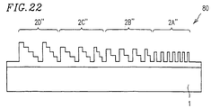
- FIG. 22 is a cross sectional view of such a diffractive optical device 80 .
- the top surface of the substrate 1 is not exposed.
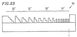
- Figure 23 is a cross sectional view of a diffractive optical device 90 having a grating pattern formed using a positive resist.
- the shape of grating elements substantially contributing to diffraction is the same whether a negative or a positive resist is used.
- the number of the phase levels changes in accordance with the grating period.
- the diffraction efficiency is improved in the entire device, especially for light incident at an offset angle with respect to the vertical direction to the top surface of the substrate.
- the grating elements are easily produced even in an area where the grating period is relatively small.
- the duty ratio regarding each cross section is set to be optimum in accordance with the grating period. In this manner, the diffraction efficiency of the light incident at an offset angle is improved even in an area where the grating period is relatively small. Further, by changing the height of the grating elements as well as the duty ratio in accordance with the grating period, the diffraction efficiency can be uniform in the entire device. As a result, light distribution in a spot where the light is collected can be constant.
Landscapes
- Physics & Mathematics (AREA)
- General Physics & Mathematics (AREA)
- Optics & Photonics (AREA)
- Engineering & Computer Science (AREA)
- Microelectronics & Electronic Packaging (AREA)
- Diffracting Gratings Or Hologram Optical Elements (AREA)
Claims (29)
- Dispositif optique de diffraction (10) comprenant :caractérisé par les caractéristiques suivantes :une source de lumière destinée à générer de la lumière d'au moins une longueur d'onde λ0 devant être diffractée,un substrat (1) destiné à permettre la transmission au travers de celui-ci de la lumière de longueur d'onde λ0 devant être diffractée, etune section de réseau (2) située sur le substrat et comprenant une pluralité d'éléments de réseau (21) présentant chacun des niveaux de phase discrets multiples,la pluralité des éléments de réseau (21) comprenant une première pluralité (2A) d'éléments de réseau (21) présentant un premier niveau de phase, et une seconde pluralité (2B) d'éléments de réseau (21) présentant un second niveau de phase différent dudit premier niveau de phase,dans lequel la pluralité des éléments de réseau (21) est agencée suivant des périodes de réseau différentes dans des zones différentes de la surface du substrat (1),la seconde pluralité (2B) des éléments de réseau (1) est agencée suivant des périodes plus grandes que ladite période.la première pluralité (2A) des éléments de réseau (21) est agencée suivant des périodes plus petites que la période qui fait que l'efficacité de diffraction de la première pluralité (2A) des éléments de réseau (21) soit égale à celle de la seconde pluralité (2B) des éléments de réseau (21) lorsque ladite lumière de longueur d'onde λ0 est incidente suivant un angle décalé par rapport à la direction verticale d'un plan de disposition de la pluralité des éléments de réseau (21),
- Dispositif optique de diffraction selon la revendication 1, caractérisé en ce que le nombre des niveaux de phase devient progressivement plus petit à mesure que les périodes de réseau diminuent.
- Dispositif optique de diffraction (10) selon la revendication 2, caractérisé en ce quele nombre des niveaux de phase est d'au moins trois dans une zone où la période de réseau est au moins une première valeur obtenue en multipliant ladite longueur d'onde λ0 par un premier nombre prescrit,le nombre des niveaux de phase est de deux dans une zone où la période de réseau est inférieure à la première valeur, etle premier nombre prescrit est pratiquement compris entre 1,5 et 3.
- Dispositif optique de diffraction (10) selon la revendication 3, caractérisé en ce que la section de réseau (2) présente un rapport cyclique qui est pratiquement entre 0,15 et 0,5 dans la zone où la période de réseau est inférieure à la première valeur.
- Dispositif optique de diffraction (10) selon la revendication 3, caractérisé en ce quele nombre des niveaux de phase est d'au moins quatre dans une zone où la période de réseau est au moins une seconde valeur obtenue en multipliant ladite longueur d'onde λ0 par un second nombre prescrit,le nombre des niveaux de phase est de trois dans une zone où la période de réseau est plus petite que la seconde valeur et au moins la première valeur, etla seconde valeur est pratiquement entre deux et cinq et est supérieure au premier nombre prescrit.
- Dispositif optique de diffraction (10) selon la revendication 5, caractérisé en ce quele nombre des niveaux de phase est d'au moins cinq dans une zone où la période de réseau est au moins une troisième valeur obtenue en multipliant ladite longueur d'onde λ0 par un troisième nombre prescrit,le nombre des niveaux de phase est de quatre dans une zone où la période de réseau est plus petite que la troisième valeur et au moins la seconde valeur, etla troisième valeur est pratiquement entre quatre et sept et est supérieure au second nombre prescrit.
- Dispositif optique de diffraction (10) selon l'une des revendications 1 à 6, caractérisé en ce que les éléments de réseau (21) présentent des hauteurs différentes conformément à leur nombre de niveaux de phase.
- Dispositif optique de diffraction (10) selon l'une des revendications 1 à 7, caractérisé en ce que le niveau le plus bas parmi les niveaux de phase discrets multiples est la surface du substrat (1).
- Dispositif optique de diffraction (10) selon l'une des revendications 1 à 8, caractérisé en ce que la période de réseau la plus petite est supérieure à 1/2 n de ladite longueur d'onde λ0, dans lequel n est l'indice de réfraction du substrat (1), et en ce que le rapport cyclique de la section de réseau (2) varie en fonction des périodes de réseau.
- Dispositif optique de diffraction (10) selon l'une des revendications 1 à 9, caractérisé en ce que les éléments de réseau (21) sont agencés symétriquement par rapport au centre de celui-ci, et sont incurvés suivant une direction identique, et en ce que la période de réseau devient progressivement plus petite selon ladite direction.
- Dispositif optique de diffraction (20) selon l'une des revendications 1 à 9, caractérisé en ce que la pluralité d'éléments de réseau (22) est étendue en lignes droites suivant une direction identique, etla période de réseau varie dans une direction qui est perpendiculaire à la direction selon laquelle les éléments de réseau (22) sont étendus.
- Dispositif optique de diffraction (70) selon l'une des revendications 1 à 11, caractérisé en ce quela section de réseau (20) est recouverte d'un film mince (7).
- Dispositif optique de diffraction (70) selon la revendication 12, caractérisé en ce que le film mince (7) est réfléchissant.
- Dispositif optique de diffraction (70) selon la revendication 12, caractérisé en ce que le film mince (7) est un film anti-réfléchissant.
- Dispositif optique de diffraction (10) selon l'une des revendications 1 à 14, caractérisé en ce que le substrat (1) comprend une région de guide de lumière (12) destinée à faire se propager ladite lumière.
- Dispositif optique de diffraction (10) selon l'une des revendications 1 à 15, caractérisé en ce que le premier niveau de phase est plus petit que le second niveau de phase.
- Dispositif optique de diffraction (60) comprenant :caractérisé en ce queune source de lumière destinée à générer de la lumière d'au moins une longueur d'onde λ0 devant être diffractée,un substrat (1) destiné à permettre la transmission au travers de celui-ci d'une lumière à une longueur d'onde λ0 devant être diffractée, etune section de réseau (2) située sur le substrat (1) et comprenant une pluralité d'éléments de réseau (26),dans lequel la pluralité d'éléments de réseau (26) comprend une première pluralité d'éléments de réseau présentant un premier rapport cyclique, et une seconde pluralité d'éléments de réseau présentant un second rapport cyclique différent dudit premier rapport cyclique,dans lequel la pluralité d'éléments de réseau (26) est agencée suivant des périodes de réseau différentes et des zones différentes de la surface du substrat (1),la période de réseau la plus petite est supérieure à 1/2 n de ladite longueur d'onde λ0, dans lequel n est l'indice de réfraction du substrat,la première pluralité d'éléments de réseau (26) est agencée suivant des périodes plus petites que la période qui rend l'efficacité de diffraction de la première pluralité d'éléments de réseau égale à celle de la seconde pluralité d'éléments de réseau (26) lorsque ladite lumière de longueur d'onde λ0 est incidente suivant un angle décalé par rapport à la direction d'un plan de disposition de la pluralité d'éléments de réseau (26),la seconde pluralité d'éléments de réseau est agencée suivant des périodes plus grandes que ladite période.
- Dispositif optique de diffraction (60) selon la revendication 17, caractérisé en ce que le rapport cyclique est inférieur à 0,5 dans une zone où la période de réseau est inférieure à trois à quatre fois ladite longueur d'onde λ0.
- Dispositif optique de diffraction (60) selon la revendication 18, caractérisé en ce que le rapport cyclique devient progressivement plus petit à mesure que la période de réseau diminue.
- Dispositif optique de diffraction (60) selon l'une des revendications 17 à 19, caractérisé en ce que la pluralité d'éléments de réseau (26) présente des hauteurs différentes qui varient en fonction des périodes de réseau.
- Dispositif optique de diffraction (60) selon la revendication 20, caractérisé en ce que la hauteur de la pluralité d'éléments de réseau (26) devient progressivement plus petite conformément à une diminution de la période de réseau dans une zone où la période de réseau est inférieure à trois à quatre fois ladite longueur d'onde λ0.
- Dispositif optique de diffraction (60) selon l'une des revendications 17 à 21, caractérisé en ce que les éléments de réseau (26) sont agencés symétriquement par rapport au centre de celui-ci et sont incurvés suivant une direction identique, et en ce que la période du réseau devient progressivement plus petite selon ladite direction.
- Dispositif optique de diffraction (60) selon l'une des revendications 17 à 21, caractérisé en ce quela pluralité d'éléments de réseau est étendue suivant des lignes droites dans une direction identique, et en ce que la période du réseau varie suivant une direction qui est perpendiculaire à ladite direction selon laquelle les éléments de réseau sont étendus.
- Dispositif optique de diffraction (60) selon l'une des revendications 17 à 23, caractérisé en ce que la section de réseau (2) est recouverte d'un film mince (7).
- Dispositif optique de diffraction (60) selon la revendication 24, caractérisé en ce que le film mince (7) est réfléchissant.
- Dispositif optique de diffraction (60) selon la revendication 24, caractérisé en ce que le film mince (7) est non-réfléchissant.
- Dispositif optique de diffraction (60) selon l'une des revendications 17 à 26, caractérisé en ce que le substrat (1) comprend une région de guide de lumière destinée à faire se propager la lumière.
- Dispositif optique de diffraction (60) selon l'une des revendications 17 à 27, caractérisé en ce que les éléments de réseau (26) dans une partie de la section de réseau présentent au moins trois niveaux de phase discrets.
- Dispositif optique de diffraction (60) selon l'une des revendications 17 à 28, caractérisé en ce que le premier rapport cyclique est plus petit que le second rapport cyclique.
Applications Claiming Priority (4)
| Application Number | Priority Date | Filing Date | Title |
|---|---|---|---|
| JP25964093A JP3189922B2 (ja) | 1993-10-18 | 1993-10-18 | 回折光学素子 |
| JP259639/93 | 1993-10-18 | ||
| JP25963993A JP3214964B2 (ja) | 1993-10-18 | 1993-10-18 | 回折光学素子 |
| JP259640/93 | 1993-10-18 |
Publications (3)
| Publication Number | Publication Date |
|---|---|
| EP0649037A2 EP0649037A2 (fr) | 1995-04-19 |
| EP0649037A3 EP0649037A3 (fr) | 1995-05-31 |
| EP0649037B1 true EP0649037B1 (fr) | 1998-06-03 |
Family
ID=26544217
Family Applications (1)
| Application Number | Title | Priority Date | Filing Date |
|---|---|---|---|
| EP94116398A Expired - Lifetime EP0649037B1 (fr) | 1993-10-18 | 1994-10-18 | Dispositif optique de diffraction |
Country Status (4)
| Country | Link |
|---|---|
| US (2) | US5561558A (fr) |
| EP (1) | EP0649037B1 (fr) |
| CN (1) | CN1145048C (fr) |
| DE (1) | DE69410732T2 (fr) |
Families Citing this family (108)
| Publication number | Priority date | Publication date | Assignee | Title |
|---|---|---|---|---|
| DE4421392A1 (de) * | 1994-06-18 | 1995-12-21 | Karlsruhe Forschzent | Gitterstruktur und deren Verwendung |
| US5905571A (en) * | 1995-08-30 | 1999-05-18 | Sandia Corporation | Optical apparatus for forming correlation spectrometers and optical processors |
| IL115295A0 (en) | 1995-09-14 | 1996-12-05 | Yeda Res & Dev | Multilevel diffractive optical element |
| US6021000A (en) | 1996-07-09 | 2000-02-01 | Asahi Kogaku Kogyo Kabushiki Kaisha | Beam splitting diffractive optical element |
| FR2753539B1 (fr) * | 1996-09-18 | 1998-10-23 | Commissariat Energie Atomique | Reseau de diffraction focalisant de tres grande efficacite et procede de fabrication de ce reseau |
| JP3408112B2 (ja) | 1997-04-30 | 2003-05-19 | キヤノン株式会社 | 回折光学素子を有した光学部材及びそれを用いた光学系 |
| US6469827B1 (en) * | 1998-08-06 | 2002-10-22 | Euv Llc | Diffraction spectral filter for use in extreme-UV lithography condenser |
| FI106323B (fi) * | 1998-12-30 | 2001-01-15 | Nokia Mobile Phones Ltd | Taustavalaistuksen valonjohdin litteälle näytölle |
| US6993222B2 (en) * | 1999-03-03 | 2006-01-31 | Rj Mears, Llc | Optical filter device with aperiodically arranged grating elements |
| GB9905196D0 (en) * | 1999-03-05 | 1999-04-28 | Fujitsu Telecommunications Eur | Aperiodic gratings |
| GB2386254A (en) | 1999-03-05 | 2003-09-10 | Nanovis Llc | Superlattices |
| US6330118B1 (en) | 1999-04-08 | 2001-12-11 | Aerial Imaging Corporation | Dual focus lens with extended depth of focus |
| FI107085B (fi) | 1999-05-28 | 2001-05-31 | Ics Intelligent Control System | Valopaneeli |
| FI106992B (fi) | 1999-05-28 | 2001-05-15 | Ics Intelligent Control System | Valo-opaste |
| US6728034B1 (en) * | 1999-06-16 | 2004-04-27 | Matsushita Electric Industrial Co., Ltd. | Diffractive optical element that polarizes light and an optical pickup using the same |
| KR100318903B1 (ko) | 2000-01-14 | 2001-12-29 | 윤종용 | 장주기 광섬유 격자 |
| US6466371B1 (en) | 2000-01-26 | 2002-10-15 | Aerial Imaging Corporation | Diffractive lens with gratings modified to offset effects caused by holding the lens at an angle with respect to a light source |
| JP3920001B2 (ja) * | 2000-03-24 | 2007-05-30 | フジノン株式会社 | 回折型レンズおよびこれを用いた光ピックアップ装置 |
| JP2001343512A (ja) * | 2000-05-31 | 2001-12-14 | Canon Inc | 回折光学素子及びそれを有する光学系 |
| IL136849A (en) * | 2000-06-18 | 2004-09-27 | Beamus Ltd | Optical dynamic devices particularly for beam steering and optical communication |
| US6810176B2 (en) * | 2000-08-07 | 2004-10-26 | Rosemount Inc. | Integrated transparent substrate and diffractive optical element |
| US7145721B2 (en) * | 2000-11-03 | 2006-12-05 | Mems Optical, Inc. | Anti-reflective structures |
| US7050675B2 (en) * | 2000-11-27 | 2006-05-23 | Advanced Interfaces, Llc | Integrated optical multiplexer and demultiplexer for wavelength division transmission of information |
| US6490393B1 (en) | 2000-11-27 | 2002-12-03 | Advanced Interfaces, Llc | Integrated optical multiplexer and demultiplexer for wavelength division transmission of information |
| US6788847B2 (en) * | 2001-04-05 | 2004-09-07 | Luxtera, Inc. | Photonic input/output port |
| DE10123230A1 (de) * | 2001-05-12 | 2002-11-28 | Zeiss Carl | Diffraktives optisches Element sowie optische Anordnung mit einem diffraktiven optischen Element |
| US8909595B2 (en) | 2001-08-01 | 2014-12-09 | T-System, Inc. | Method for entering, recording, distributing and reporting data |
| US8898106B2 (en) * | 2001-08-01 | 2014-11-25 | T-System, Inc. | Method for entering, recording, distributing and reporting data |
| US6990257B2 (en) * | 2001-09-10 | 2006-01-24 | California Institute Of Technology | Electronically biased strip loaded waveguide |
| US7082235B2 (en) * | 2001-09-10 | 2006-07-25 | California Institute Of Technology | Structure and method for coupling light between dissimilar waveguides |
| WO2003023824A2 (fr) * | 2001-09-10 | 2003-03-20 | California Institute Of Technology | Modulateur base sur une cavite resonante accordable |
| CN1313846C (zh) * | 2001-10-05 | 2007-05-02 | 松下电器产业株式会社 | 衍射光学元件及使用了该衍射光学元件的光学头 |
| JP4454898B2 (ja) * | 2001-12-17 | 2010-04-21 | キヤノン株式会社 | 走査光学系及びそれを有する画像形成装置 |
| US6987901B2 (en) * | 2002-03-01 | 2006-01-17 | Rosemount, Inc. | Optical switch with 3D waveguides |
| DE10216562C1 (de) | 2002-04-05 | 2003-12-11 | Ovd Kinegram Ag Zug | Sicherheitselement mit Mikro- und Makrostrukturen |
| US20060012880A1 (en) * | 2002-05-02 | 2006-01-19 | Law Benjamin P | Optical device with refractive and diffractive properties |
| JP4310080B2 (ja) * | 2002-06-17 | 2009-08-05 | キヤノン株式会社 | 回折光学素子およびこれを備えた光学系、光学装置 |
| US6993236B1 (en) | 2002-06-24 | 2006-01-31 | Luxtera, Inc. | Polysilicon and silicon dioxide light scatterers for silicon waveguides on five layer substrates |
| US7010208B1 (en) | 2002-06-24 | 2006-03-07 | Luxtera, Inc. | CMOS process silicon waveguides |
| US7110180B2 (en) * | 2002-10-09 | 2006-09-19 | Ricoh Company, Ltd. | Diffraction grating, method of fabricating diffraction optical element, optical pickup device, and optical disk drive |
| US6747785B2 (en) * | 2002-10-24 | 2004-06-08 | Hewlett-Packard Development Company, L.P. | MEMS-actuated color light modulator and methods |
| US20040096782A1 (en) * | 2002-11-14 | 2004-05-20 | Trott Gary R. | Hermetic seal for diffractive elements |
| US7245803B2 (en) * | 2003-02-11 | 2007-07-17 | Luxtera, Inc. | Optical waveguide grating coupler |
| US7260289B1 (en) | 2003-02-11 | 2007-08-21 | Luxtera, Inc. | Optical waveguide grating coupler with varying scatter cross sections |
| US7184625B2 (en) * | 2003-02-11 | 2007-02-27 | Luxtera, Inc | Optical waveguide grating coupler incorporating reflective optical elements and anti-reflection elements |
| US7006732B2 (en) * | 2003-03-21 | 2006-02-28 | Luxtera, Inc. | Polarization splitting grating couplers |
| DE10322239B4 (de) * | 2003-05-17 | 2011-06-30 | Carl Zeiss SMT GmbH, 73447 | Geblazetes diffraktives optisches Element sowie Projektionsobjektiv mit einem solchen Element |
| US7083106B2 (en) | 2003-09-05 | 2006-08-01 | Cytyc Corporation | Locally storing biological specimen data to a slide |
| US7773836B2 (en) | 2005-12-14 | 2010-08-10 | Luxtera, Inc. | Integrated transceiver with lightpipe coupler |
| EP1736803A1 (fr) * | 2004-04-13 | 2006-12-27 | Matsushita Electric Industrial Co., Ltd. | Élément de condensation et dispositif de formation d'images à semiconducteur |
| EP1751593B1 (fr) | 2004-04-30 | 2019-03-06 | Modilis Holdings LLC | Element lumineux ultramince |
| US7251208B2 (en) * | 2004-06-01 | 2007-07-31 | Matsushita Electric Industrial Co., Ltd. | Optical pick-up system for use in an optical disk device including use of improved gratings with more efficient beam diffraction |
| US7315679B2 (en) * | 2004-06-07 | 2008-01-01 | California Institute Of Technology | Segmented waveguide structures |
| US7667286B2 (en) * | 2004-09-01 | 2010-02-23 | Panasonic Corporation | Light-collecting device, solid-state imaging apparatus and method of manufacturing thereof |
| US7682062B2 (en) * | 2004-09-09 | 2010-03-23 | Nanogate Advanced Materials Gmbh | Illuminating device |
| US20060066948A1 (en) * | 2004-09-24 | 2006-03-30 | Matsushita Electric Industrial Co., Ltd. | Multi-level and gray-level diffraction gratings |
| CN1782743A (zh) * | 2004-12-04 | 2006-06-07 | 鸿富锦精密工业(深圳)有限公司 | 镜片 |
| KR100659293B1 (ko) * | 2005-01-20 | 2006-12-20 | 삼성전자주식회사 | 회절소자 및 이를 포함하는 광픽업장치 |
| JP5048930B2 (ja) * | 2005-06-08 | 2012-10-17 | ラピスセミコンダクタ株式会社 | 回折光学素子,および,回折光学素子の製造方法 |
| JP4456040B2 (ja) * | 2005-06-17 | 2010-04-28 | パナソニック株式会社 | 固体撮像素子 |
| US7826688B1 (en) | 2005-10-21 | 2010-11-02 | Luxtera, Inc. | Enhancing the sensitivity of resonant optical modulating and switching devices |
| CN101313234B (zh) * | 2005-11-18 | 2011-01-05 | 纳诺科普有限公司 | 制造衍射光栅元件的方法 |
| KR100818272B1 (ko) * | 2006-08-21 | 2008-04-01 | 삼성전자주식회사 | 색분산이 개선된 홀로그래픽 도광판 |
| WO2008110239A1 (fr) * | 2007-03-15 | 2008-09-18 | Carl Zeiss Smt Ag | Composant diffractif, agencement d'interféromètre, procédé de qualification de réseau de diffraction double, procédé de fabrication d'un élément optique, et procédé d'interférométrie |
| CN101578537B (zh) * | 2007-11-13 | 2012-07-04 | 松下电器产业株式会社 | 薄膜及发光装置 |
| JP4535121B2 (ja) * | 2007-11-28 | 2010-09-01 | セイコーエプソン株式会社 | 光学素子及びその製造方法、液晶装置、電子機器 |
| WO2011008216A1 (fr) | 2009-07-17 | 2011-01-20 | Hewlett-Packard Development Company, L.P. | Réflecteurs à réseau non périodiques dotés dune puissance de focalisation et procédés de fabrication de ces réflecteurs à réseau |
| EP2480917A4 (fr) | 2009-09-23 | 2013-05-29 | Hewlett Packard Development Co | Dispositifs optiques basés sur des grilles de diffraction |
| US20110085232A1 (en) * | 2009-10-08 | 2011-04-14 | The Penn State Research Foundation | Multi-spectral filters, mirrors and anti-reflective coatings with subwavelength periodic features for optical devices |
| WO2011093893A1 (fr) | 2010-01-29 | 2011-08-04 | Hewlett-Packard Development Company, L.P. | Dispositifs optiques basés sur des réseaux sub-longueur d'onde non périodiques |
| SG184134A1 (en) * | 2010-04-12 | 2012-11-29 | 3M Innovative Properties Co | Optical stack and lightguides |
| WO2011129814A1 (fr) * | 2010-04-13 | 2011-10-20 | Hewlett-Packard Development Company, L.P. | Commande de réponse de phase dans un dispositif optique à réseau de diffraction de sous-longueur d'onde |
| US8534900B2 (en) * | 2011-03-25 | 2013-09-17 | Unipixel Displays, Inc. | Interleaved lighting system for 2D-3D display having orthogonally arranged light extraction features |
| WO2012164781A1 (fr) | 2011-05-30 | 2012-12-06 | パナソニック株式会社 | Élément optique diffractif et procédé de fabrication |
| DE102014219663A1 (de) * | 2014-09-29 | 2016-03-31 | Ihp Gmbh - Innovations For High Performance Microelectronics / Leibniz-Institut Für Innovative Mikroelektronik | Photonisch integrierter Chip, optisches Bauelement mit photonisch integriertem Chip und Verfahren zu deren Herstellung |
| JP6824171B2 (ja) * | 2015-01-10 | 2021-02-10 | レイア、インコーポレイテッドLeia Inc. | 制御された回折カップリング効率を有する回折格子ベースの背面照明 |
| KR102214345B1 (ko) * | 2015-01-10 | 2021-02-09 | 레이아 인코포레이티드 | 2차원/3차원(2d/3d) 전환가능 디스플레이 백라이트 및 전자 디스플레이 |
| KR102200059B1 (ko) * | 2015-01-19 | 2021-01-08 | 레이아 인코포레이티드 | 반사 아일랜드를 채용하는 단일 방향 격자-기반 백라이팅 |
| US10054720B2 (en) * | 2015-02-02 | 2018-08-21 | Apple Inc. | Fresnel lens barrier rings |
| ES2805551T3 (es) | 2015-03-30 | 2021-02-12 | Leia Inc | Pantalla electrónica conmutable entre modos 2D/3D y con retroiluminación de doble capa |
| US10423002B2 (en) | 2015-06-17 | 2019-09-24 | Maxell, Ltd. | Imaging apparatus capable of generating an image using moire without a lens |
| JP6709278B2 (ja) * | 2015-09-05 | 2020-06-10 | レイア、インコーポレイテッドLeia Inc. | 多色格子カップリングされた背面照明 |
| CN108702440B (zh) * | 2016-02-26 | 2021-06-29 | 株式会社日立制作所 | 摄像装置 |
| WO2017151291A1 (fr) * | 2016-03-04 | 2017-09-08 | Applied Materials, Inc. | Procédé de fabrication de polariseur à grille métallique |
| US11179802B2 (en) * | 2016-07-14 | 2021-11-23 | Mitsubishi Electric Corporation | Laser machining head and laser machining apparatus |
| FR3059110A1 (fr) | 2016-11-21 | 2018-05-25 | Stmicroelectronics (Crolles 2) Sas | Diffuseur optique et son procede de fabrication |
| US10473834B2 (en) * | 2016-11-21 | 2019-11-12 | Stmicroelectronics (Research & Development) Limited | Wafer level microstructures for an optical lens |
| CN106680922B (zh) * | 2017-03-08 | 2019-03-12 | 福建中科晶创光电科技有限公司 | 一种紫外胶光栅的制作方法 |
| CN106842598B (zh) * | 2017-03-17 | 2019-09-06 | 京东方科技集团股份有限公司 | 显示切换装置、显示器和电子设备 |
| FI128376B (en) * | 2017-06-02 | 2020-04-15 | Dispelix Oy | Process for the preparation of a diffractive grating with varying efficiency and a diffraction grating |
| FI128410B (en) | 2017-06-02 | 2020-04-30 | Dispelix Oy | Method for producing a height modulated optical diffraction grating |
| US11086059B2 (en) * | 2017-06-13 | 2021-08-10 | Vuzix Corporation | Image light guide with expanded light distribution overlapping gratings |
| CN107193070B (zh) * | 2017-08-01 | 2020-07-28 | 京东方科技集团股份有限公司 | 一种光场调制层、背光结构及显示装置 |
| WO2019125390A1 (fr) | 2017-12-18 | 2019-06-27 | Leia Inc. | Rétroéclairage à mode commutable, dispositif d'affichage, et procédé |
| US10802117B2 (en) | 2018-01-24 | 2020-10-13 | Facebook Technologies, Llc | Systems and methods for optical demodulation in a depth-sensing device |
| US10805594B2 (en) | 2018-02-08 | 2020-10-13 | Facebook Technologies, Llc | Systems and methods for enhanced depth sensor devices |
| US10735640B2 (en) * | 2018-02-08 | 2020-08-04 | Facebook Technologies, Llc | Systems and methods for enhanced optical sensor devices |
| CA3089955C (fr) | 2018-03-01 | 2022-10-18 | Leia Inc. | Affichage multivue statique et procede utilisant une lumiere guidee collimatee |
| WO2020080169A1 (fr) * | 2018-10-15 | 2020-04-23 | Agc株式会社 | Élément optique diffractif et système optique d'illumination |
| US11391957B2 (en) | 2018-10-29 | 2022-07-19 | Stmicroelectronics (Research & Development) Limited | Embedded transmissive diffractive optical elements |
| TWI682160B (zh) * | 2018-12-11 | 2020-01-11 | 國立交通大學 | 生物訊號分析元件、生物感測裝置、感測方法以及生物訊號分析元件的製作方法 |
| US11487053B2 (en) * | 2019-02-26 | 2022-11-01 | Ii-Vi Delaware, Inc. | Partially etched phase-transforming optical element |
| CN114167664A (zh) * | 2020-08-21 | 2022-03-11 | 超聚变数字技术有限公司 | 光学镜头和终端设备 |
| US11719885B2 (en) * | 2020-10-14 | 2023-08-08 | Taiwan Semiconductor Manufacturing Company, Ltd. | Apparatus for optical coupling and system for communication |
| TWI741924B (zh) * | 2020-12-29 | 2021-10-01 | 新唐科技股份有限公司 | 菲涅耳透鏡之形成方法 |
| US11899223B2 (en) | 2021-05-24 | 2024-02-13 | Visera Technologies Company Limited | Optical device |
| US12140802B2 (en) | 2021-05-28 | 2024-11-12 | Taiwan Semiconductor Manufacturing Co., Ltd. | 1D apodized grating devices and methods for suppressing optical noise |
| CN114047569B (zh) * | 2021-11-17 | 2024-10-22 | 佛山紫熙慧众科技有限公司 | 一种实现一字线光斑的渐变周期光栅衍射元件及方法 |
Family Cites Families (14)
| Publication number | Priority date | Publication date | Assignee | Title |
|---|---|---|---|---|
| DE276740C (fr) * | ||||
| DE2657246C2 (de) * | 1976-12-17 | 1978-09-28 | Hoechst Ag, 6000 Frankfurt | Original eines Informationsträgers, Verfahren zum Herstellen des Originals, Verfahren zum Herstellen einer Matrize zum Prägen des Originals sowie Informa tionsträger, der mit der Matrize hergestellt ist |
| DE3536497A1 (de) * | 1984-10-16 | 1986-04-17 | Mitsubishi Denki K.K., Tokio/Tokyo | Vorrichtung zur erfassung von fokussierungsfehlern in einer kopfanordnung fuer optische scheiben |
| JPS62296102A (ja) * | 1986-06-17 | 1987-12-23 | Nec Corp | 導波路グレ−テイング結合器 |
| US4798446A (en) * | 1987-09-14 | 1989-01-17 | The United States Of America As Represented By The United States Department Of Energy | Aplanatic and quasi-aplanatic diffraction gratings |
| US5161059A (en) * | 1987-09-21 | 1992-11-03 | Massachusetts Institute Of Technology | High-efficiency, multilevel, diffractive optical elements |
| US4936665A (en) * | 1987-10-25 | 1990-06-26 | Whitney Theodore R | High resolution imagery systems and methods |
| US5283690A (en) * | 1989-04-04 | 1994-02-01 | Sharp Kabushiki Kaisha | Optical diffraction grating element |
| DE69017852T2 (de) * | 1989-12-04 | 1995-08-10 | Canon Kk | Optisches Kopplergerät mit wellenlängeselektivem optischem Koppler. |
| US5227915A (en) * | 1990-02-13 | 1993-07-13 | Holo-Or Ltd. | Diffractive optical element |
| EP0515567A4 (en) * | 1990-02-13 | 1993-02-17 | Holo-Or Ltd. | Diffractive optical element |
| JPH04211202A (ja) * | 1990-03-19 | 1992-08-03 | Canon Inc | 反射型回折格子および該回折格子を用いた装置 |
| US5073007A (en) * | 1990-06-11 | 1991-12-17 | Holo-Or Ltd. | Diffractive optical element |
| JPH0694939A (ja) * | 1992-09-09 | 1994-04-08 | Fuji Photo Film Co Ltd | 光導波路素子 |
-
1994
- 1994-10-17 US US08/323,927 patent/US5561558A/en not_active Expired - Lifetime
- 1994-10-18 CN CNB941128148A patent/CN1145048C/zh not_active Expired - Fee Related
- 1994-10-18 DE DE69410732T patent/DE69410732T2/de not_active Expired - Fee Related
- 1994-10-18 EP EP94116398A patent/EP0649037B1/fr not_active Expired - Lifetime
-
1996
- 1996-04-04 US US08/627,442 patent/US5742433A/en not_active Expired - Lifetime
Also Published As
| Publication number | Publication date |
|---|---|
| CN1145048C (zh) | 2004-04-07 |
| DE69410732D1 (de) | 1998-07-09 |
| US5742433A (en) | 1998-04-21 |
| DE69410732T2 (de) | 1999-01-21 |
| EP0649037A2 (fr) | 1995-04-19 |
| EP0649037A3 (fr) | 1995-05-31 |
| US5561558A (en) | 1996-10-01 |
| CN1116719A (zh) | 1996-02-14 |
Similar Documents
| Publication | Publication Date | Title |
|---|---|---|
| EP0649037B1 (fr) | Dispositif optique de diffraction | |
| EP0468410B1 (fr) | Lentille optique diffractive | |
| US7965447B2 (en) | Optical substrate and method of making | |
| EP0656549A2 (fr) | Eléments optiques et leur méthode de fabrication | |
| US10823889B2 (en) | Partially etched phase-transforming optical element | |
| EP0367241A2 (fr) | Système de lentille optique diffractif faisant une image | |
| US20040100699A1 (en) | Directional diffuser | |
| US20040076374A1 (en) | Amplitude and phase control in distributed optical structures | |
| EP0582958B1 (fr) | Dispositif laser à semi-conducteur, dispositif optique et méthode de sa fabrication | |
| US11921306B2 (en) | Diffraction grating array for wide-angle illumination | |
| US6415073B1 (en) | Wavelength division multiplexing/demultiplexing devices employing patterned optical components | |
| US7860352B2 (en) | Light-collecting apparatus and contact-type solid-state imaging apparatus using the same | |
| US5258862A (en) | Rotating disc optical synchronization system using binary diffractive optical elements | |
| US5291319A (en) | Rotating disc optical synchronization system using binary diffractive optical elements | |
| JP3189922B2 (ja) | 回折光学素子 | |
| US5907435A (en) | Laser beam optical focusing system of two symmetrical diffractive optical elements | |
| US4595290A (en) | Device for measuring light incident on an optical system | |
| JP3214964B2 (ja) | 回折光学素子 | |
| Blattner et al. | Rigorous diffraction theory applied to microlenses | |
| EP0219845B1 (fr) | Réseau de phase du type combiné à créneau et par réfraction | |
| EP1316835A2 (fr) | Système micro-opto-électromécanique (MOEMS) avec des plaques à zones de Fresnel réfléchissantes | |
| US5161058A (en) | Focusing screen | |
| US5914814A (en) | Telecentric laser beam optical focusing system of two diffractive optical elements | |
| EP0632296A1 (fr) | Elément optique diffractive binaire pour filtrer l'amplitude et la phase | |
| JP3711680B2 (ja) | ビーム整形装置 |
Legal Events
| Date | Code | Title | Description |
|---|---|---|---|
| PUAI | Public reference made under article 153(3) epc to a published international application that has entered the european phase |
Free format text: ORIGINAL CODE: 0009012 |
|
| PUAL | Search report despatched |
Free format text: ORIGINAL CODE: 0009013 |
|
| 17P | Request for examination filed |
Effective date: 19950217 |
|
| AK | Designated contracting states |
Kind code of ref document: A2 Designated state(s): DE FR GB |
|
| AK | Designated contracting states |
Kind code of ref document: A3 Designated state(s): DE FR GB |
|
| 17Q | First examination report despatched |
Effective date: 19950911 |
|
| GRAG | Despatch of communication of intention to grant |
Free format text: ORIGINAL CODE: EPIDOS AGRA |
|
| GRAG | Despatch of communication of intention to grant |
Free format text: ORIGINAL CODE: EPIDOS AGRA |
|
| GRAH | Despatch of communication of intention to grant a patent |
Free format text: ORIGINAL CODE: EPIDOS IGRA |
|
| GRAH | Despatch of communication of intention to grant a patent |
Free format text: ORIGINAL CODE: EPIDOS IGRA |
|
| GRAH | Despatch of communication of intention to grant a patent |
Free format text: ORIGINAL CODE: EPIDOS IGRA |
|
| GRAA | (expected) grant |
Free format text: ORIGINAL CODE: 0009210 |
|
| AK | Designated contracting states |
Kind code of ref document: B1 Designated state(s): DE FR GB |
|
| REF | Corresponds to: |
Ref document number: 69410732 Country of ref document: DE Date of ref document: 19980709 |
|
| ET | Fr: translation filed | ||
| PLBE | No opposition filed within time limit |
Free format text: ORIGINAL CODE: 0009261 |
|
| STAA | Information on the status of an ep patent application or granted ep patent |
Free format text: STATUS: NO OPPOSITION FILED WITHIN TIME LIMIT |
|
| 26N | No opposition filed | ||
| REG | Reference to a national code |
Ref country code: GB Ref legal event code: IF02 |
|
| PGFP | Annual fee paid to national office [announced via postgrant information from national office to epo] |
Ref country code: FR Payment date: 20051010 Year of fee payment: 12 |
|
| PGFP | Annual fee paid to national office [announced via postgrant information from national office to epo] |
Ref country code: GB Payment date: 20051012 Year of fee payment: 12 |
|
| PGFP | Annual fee paid to national office [announced via postgrant information from national office to epo] |
Ref country code: DE Payment date: 20051014 Year of fee payment: 12 |
|
| PG25 | Lapsed in a contracting state [announced via postgrant information from national office to epo] |
Ref country code: DE Free format text: LAPSE BECAUSE OF NON-PAYMENT OF DUE FEES Effective date: 20070501 |
|
| GBPC | Gb: european patent ceased through non-payment of renewal fee |
Effective date: 20061018 |
|
| REG | Reference to a national code |
Ref country code: FR Ref legal event code: ST Effective date: 20070629 |
|
| PG25 | Lapsed in a contracting state [announced via postgrant information from national office to epo] |
Ref country code: GB Free format text: LAPSE BECAUSE OF NON-PAYMENT OF DUE FEES Effective date: 20061018 |
|
| PG25 | Lapsed in a contracting state [announced via postgrant information from national office to epo] |
Ref country code: FR Free format text: LAPSE BECAUSE OF NON-PAYMENT OF DUE FEES Effective date: 20061031 |