EP0649171A2 - Mehrchipmodul mit einem mittels eines Zwischenträger produzierten Verdrahtungsfilm - Google Patents
Mehrchipmodul mit einem mittels eines Zwischenträger produzierten Verdrahtungsfilm Download PDFInfo
- Publication number
- EP0649171A2 EP0649171A2 EP94307501A EP94307501A EP0649171A2 EP 0649171 A2 EP0649171 A2 EP 0649171A2 EP 94307501 A EP94307501 A EP 94307501A EP 94307501 A EP94307501 A EP 94307501A EP 0649171 A2 EP0649171 A2 EP 0649171A2
- Authority
- EP
- European Patent Office
- Prior art keywords
- decal
- pads
- chip
- module
- pad
- Prior art date
- Legal status (The legal status is an assumption and is not a legal conclusion. Google has not performed a legal analysis and makes no representation as to the accuracy of the status listed.)
- Withdrawn
Links
Images



Classifications
-
- H—ELECTRICITY
- H10—SEMICONDUCTOR DEVICES; ELECTRIC SOLID-STATE DEVICES NOT OTHERWISE PROVIDED FOR
- H10W—GENERIC PACKAGES, INTERCONNECTIONS, CONNECTORS OR OTHER CONSTRUCTIONAL DETAILS OF DEVICES COVERED BY CLASS H10
- H10W70/00—Package substrates; Interposers; Redistribution layers [RDL]
- H10W70/01—Manufacture or treatment
- H10W70/05—Manufacture or treatment of insulating or insulated package substrates, or of interposers, or of redistribution layers
- H10W70/093—Connecting or disconnecting other interconnections thereto or therefrom, e.g. connecting bond wires or bumps
-
- H—ELECTRICITY
- H10—SEMICONDUCTOR DEVICES; ELECTRIC SOLID-STATE DEVICES NOT OTHERWISE PROVIDED FOR
- H10W—GENERIC PACKAGES, INTERCONNECTIONS, CONNECTORS OR OTHER CONSTRUCTIONAL DETAILS OF DEVICES COVERED BY CLASS H10
- H10W70/00—Package substrates; Interposers; Redistribution layers [RDL]
- H10W70/60—Insulating or insulated package substrates; Interposers; Redistribution layers
- H10W70/611—Insulating or insulated package substrates; Interposers; Redistribution layers for connecting multiple chips together
-
- H—ELECTRICITY
- H10—SEMICONDUCTOR DEVICES; ELECTRIC SOLID-STATE DEVICES NOT OTHERWISE PROVIDED FOR
- H10W—GENERIC PACKAGES, INTERCONNECTIONS, CONNECTORS OR OTHER CONSTRUCTIONAL DETAILS OF DEVICES COVERED BY CLASS H10
- H10W70/00—Package substrates; Interposers; Redistribution layers [RDL]
- H10W70/60—Insulating or insulated package substrates; Interposers; Redistribution layers
- H10W70/62—Insulating or insulated package substrates; Interposers; Redistribution layers characterised by their interconnections
- H10W70/63—Vias, e.g. via plugs
- H10W70/635—Through-vias
-
- H—ELECTRICITY
- H10—SEMICONDUCTOR DEVICES; ELECTRIC SOLID-STATE DEVICES NOT OTHERWISE PROVIDED FOR
- H10W—GENERIC PACKAGES, INTERCONNECTIONS, CONNECTORS OR OTHER CONSTRUCTIONAL DETAILS OF DEVICES COVERED BY CLASS H10
- H10W90/00—Package configurations
-
- H—ELECTRICITY
- H10—SEMICONDUCTOR DEVICES; ELECTRIC SOLID-STATE DEVICES NOT OTHERWISE PROVIDED FOR
- H10W—GENERIC PACKAGES, INTERCONNECTIONS, CONNECTORS OR OTHER CONSTRUCTIONAL DETAILS OF DEVICES COVERED BY CLASS H10
- H10W90/00—Package configurations
- H10W90/401—Package configurations characterised by multiple insulating or insulated package substrates, interposers or RDLs
-
- H—ELECTRICITY
- H05—ELECTRIC TECHNIQUES NOT OTHERWISE PROVIDED FOR
- H05K—PRINTED CIRCUITS; CASINGS OR CONSTRUCTIONAL DETAILS OF ELECTRIC APPARATUS; MANUFACTURE OF ASSEMBLAGES OF ELECTRICAL COMPONENTS
- H05K3/00—Apparatus or processes for manufacturing printed circuits
- H05K3/10—Apparatus or processes for manufacturing printed circuits in which conductive material is applied to the insulating support in such a manner as to form the desired conductive pattern
- H05K3/20—Apparatus or processes for manufacturing printed circuits in which conductive material is applied to the insulating support in such a manner as to form the desired conductive pattern by affixing prefabricated conductor pattern
-
- H—ELECTRICITY
- H05—ELECTRIC TECHNIQUES NOT OTHERWISE PROVIDED FOR
- H05K—PRINTED CIRCUITS; CASINGS OR CONSTRUCTIONAL DETAILS OF ELECTRIC APPARATUS; MANUFACTURE OF ASSEMBLAGES OF ELECTRICAL COMPONENTS
- H05K3/00—Apparatus or processes for manufacturing printed circuits
- H05K3/40—Forming printed elements for providing electric connections to or between printed circuits
- H05K3/4038—Through-connections; Vertical interconnect access [VIA] connections
- H05K3/4084—Through-connections; Vertical interconnect access [VIA] connections by deforming at least one of the conductive layers
-
- H—ELECTRICITY
- H10—SEMICONDUCTOR DEVICES; ELECTRIC SOLID-STATE DEVICES NOT OTHERWISE PROVIDED FOR
- H10W—GENERIC PACKAGES, INTERCONNECTIONS, CONNECTORS OR OTHER CONSTRUCTIONAL DETAILS OF DEVICES COVERED BY CLASS H10
- H10W70/00—Package substrates; Interposers; Redistribution layers [RDL]
- H10W70/60—Insulating or insulated package substrates; Interposers; Redistribution layers
- H10W70/62—Insulating or insulated package substrates; Interposers; Redistribution layers characterised by their interconnections
- H10W70/65—Shapes or dispositions of interconnections
- H10W70/654—Top-view layouts
- H10W70/656—Fan-in layouts
-
- H—ELECTRICITY
- H10—SEMICONDUCTOR DEVICES; ELECTRIC SOLID-STATE DEVICES NOT OTHERWISE PROVIDED FOR
- H10W—GENERIC PACKAGES, INTERCONNECTIONS, CONNECTORS OR OTHER CONSTRUCTIONAL DETAILS OF DEVICES COVERED BY CLASS H10
- H10W70/00—Package substrates; Interposers; Redistribution layers [RDL]
- H10W70/60—Insulating or insulated package substrates; Interposers; Redistribution layers
- H10W70/67—Insulating or insulated package substrates; Interposers; Redistribution layers characterised by their insulating layers or insulating parts
- H10W70/68—Shapes or dispositions thereof
- H10W70/682—Shapes or dispositions thereof comprising holes having chips therein
-
- H—ELECTRICITY
- H10—SEMICONDUCTOR DEVICES; ELECTRIC SOLID-STATE DEVICES NOT OTHERWISE PROVIDED FOR
- H10W—GENERIC PACKAGES, INTERCONNECTIONS, CONNECTORS OR OTHER CONSTRUCTIONAL DETAILS OF DEVICES COVERED BY CLASS H10
- H10W70/00—Package substrates; Interposers; Redistribution layers [RDL]
- H10W70/60—Insulating or insulated package substrates; Interposers; Redistribution layers
- H10W70/67—Insulating or insulated package substrates; Interposers; Redistribution layers characterised by their insulating layers or insulating parts
- H10W70/68—Shapes or dispositions thereof
- H10W70/685—Shapes or dispositions thereof comprising multiple insulating layers
-
- H—ELECTRICITY
- H10—SEMICONDUCTOR DEVICES; ELECTRIC SOLID-STATE DEVICES NOT OTHERWISE PROVIDED FOR
- H10W—GENERIC PACKAGES, INTERCONNECTIONS, CONNECTORS OR OTHER CONSTRUCTIONAL DETAILS OF DEVICES COVERED BY CLASS H10
- H10W72/00—Interconnections or connectors in packages
- H10W72/071—Connecting or disconnecting
- H10W72/075—Connecting or disconnecting of bond wires
-
- H—ELECTRICITY
- H10—SEMICONDUCTOR DEVICES; ELECTRIC SOLID-STATE DEVICES NOT OTHERWISE PROVIDED FOR
- H10W—GENERIC PACKAGES, INTERCONNECTIONS, CONNECTORS OR OTHER CONSTRUCTIONAL DETAILS OF DEVICES COVERED BY CLASS H10
- H10W72/00—Interconnections or connectors in packages
- H10W72/071—Connecting or disconnecting
- H10W72/075—Connecting or disconnecting of bond wires
- H10W72/07531—Techniques
- H10W72/07532—Compression bonding, e.g. thermocompression bonding
- H10W72/07533—Ultrasonic bonding, e.g. thermosonic bonding
-
- H—ELECTRICITY
- H10—SEMICONDUCTOR DEVICES; ELECTRIC SOLID-STATE DEVICES NOT OTHERWISE PROVIDED FOR
- H10W—GENERIC PACKAGES, INTERCONNECTIONS, CONNECTORS OR OTHER CONSTRUCTIONAL DETAILS OF DEVICES COVERED BY CLASS H10
- H10W72/00—Interconnections or connectors in packages
- H10W72/071—Connecting or disconnecting
- H10W72/075—Connecting or disconnecting of bond wires
- H10W72/07551—Connecting or disconnecting of bond wires characterised by changes in properties of the bond wires during the connecting
- H10W72/07553—Connecting or disconnecting of bond wires characterised by changes in properties of the bond wires during the connecting changes in shapes
-
- H—ELECTRICITY
- H10—SEMICONDUCTOR DEVICES; ELECTRIC SOLID-STATE DEVICES NOT OTHERWISE PROVIDED FOR
- H10W—GENERIC PACKAGES, INTERCONNECTIONS, CONNECTORS OR OTHER CONSTRUCTIONAL DETAILS OF DEVICES COVERED BY CLASS H10
- H10W72/00—Interconnections or connectors in packages
- H10W72/071—Connecting or disconnecting
- H10W72/075—Connecting or disconnecting of bond wires
- H10W72/07551—Connecting or disconnecting of bond wires characterised by changes in properties of the bond wires during the connecting
- H10W72/07554—Connecting or disconnecting of bond wires characterised by changes in properties of the bond wires during the connecting changes in dispositions
-
- H—ELECTRICITY
- H10—SEMICONDUCTOR DEVICES; ELECTRIC SOLID-STATE DEVICES NOT OTHERWISE PROVIDED FOR
- H10W—GENERIC PACKAGES, INTERCONNECTIONS, CONNECTORS OR OTHER CONSTRUCTIONAL DETAILS OF DEVICES COVERED BY CLASS H10
- H10W72/00—Interconnections or connectors in packages
- H10W72/20—Bump connectors, e.g. solder bumps or copper pillars; Dummy bumps; Thermal bumps
- H10W72/29—Bond pads specially adapted therefor
-
- H—ELECTRICITY
- H10—SEMICONDUCTOR DEVICES; ELECTRIC SOLID-STATE DEVICES NOT OTHERWISE PROVIDED FOR
- H10W—GENERIC PACKAGES, INTERCONNECTIONS, CONNECTORS OR OTHER CONSTRUCTIONAL DETAILS OF DEVICES COVERED BY CLASS H10
- H10W72/00—Interconnections or connectors in packages
- H10W72/50—Bond wires
- H10W72/531—Shapes of wire connectors
- H10W72/5363—Shapes of wire connectors the connected ends being wedge-shaped
-
- H—ELECTRICITY
- H10—SEMICONDUCTOR DEVICES; ELECTRIC SOLID-STATE DEVICES NOT OTHERWISE PROVIDED FOR
- H10W—GENERIC PACKAGES, INTERCONNECTIONS, CONNECTORS OR OTHER CONSTRUCTIONAL DETAILS OF DEVICES COVERED BY CLASS H10
- H10W72/00—Interconnections or connectors in packages
- H10W72/50—Bond wires
- H10W72/531—Shapes of wire connectors
- H10W72/5366—Shapes of wire connectors the bond wires having kinks
-
- H—ELECTRICITY
- H10—SEMICONDUCTOR DEVICES; ELECTRIC SOLID-STATE DEVICES NOT OTHERWISE PROVIDED FOR
- H10W—GENERIC PACKAGES, INTERCONNECTIONS, CONNECTORS OR OTHER CONSTRUCTIONAL DETAILS OF DEVICES COVERED BY CLASS H10
- H10W72/00—Interconnections or connectors in packages
- H10W72/50—Bond wires
- H10W72/541—Dispositions of bond wires
- H10W72/5445—Dispositions of bond wires being orthogonal to a side surface of the chip, e.g. parallel arrangements
-
- H—ELECTRICITY
- H10—SEMICONDUCTOR DEVICES; ELECTRIC SOLID-STATE DEVICES NOT OTHERWISE PROVIDED FOR
- H10W—GENERIC PACKAGES, INTERCONNECTIONS, CONNECTORS OR OTHER CONSTRUCTIONAL DETAILS OF DEVICES COVERED BY CLASS H10
- H10W72/00—Interconnections or connectors in packages
- H10W72/50—Bond wires
- H10W72/541—Dispositions of bond wires
- H10W72/547—Dispositions of multiple bond wires
-
- H—ELECTRICITY
- H10—SEMICONDUCTOR DEVICES; ELECTRIC SOLID-STATE DEVICES NOT OTHERWISE PROVIDED FOR
- H10W—GENERIC PACKAGES, INTERCONNECTIONS, CONNECTORS OR OTHER CONSTRUCTIONAL DETAILS OF DEVICES COVERED BY CLASS H10
- H10W72/00—Interconnections or connectors in packages
- H10W72/50—Bond wires
- H10W72/581—Auxiliary members, e.g. flow barriers
- H10W72/583—Reinforcing structures
-
- H—ELECTRICITY
- H10—SEMICONDUCTOR DEVICES; ELECTRIC SOLID-STATE DEVICES NOT OTHERWISE PROVIDED FOR
- H10W—GENERIC PACKAGES, INTERCONNECTIONS, CONNECTORS OR OTHER CONSTRUCTIONAL DETAILS OF DEVICES COVERED BY CLASS H10
- H10W72/00—Interconnections or connectors in packages
- H10W72/90—Bond pads, in general
- H10W72/931—Shapes of bond pads
- H10W72/932—Plan-view shape, i.e. in top view
-
- H—ELECTRICITY
- H10—SEMICONDUCTOR DEVICES; ELECTRIC SOLID-STATE DEVICES NOT OTHERWISE PROVIDED FOR
- H10W—GENERIC PACKAGES, INTERCONNECTIONS, CONNECTORS OR OTHER CONSTRUCTIONAL DETAILS OF DEVICES COVERED BY CLASS H10
- H10W72/00—Interconnections or connectors in packages
- H10W72/90—Bond pads, in general
- H10W72/951—Materials of bond pads
- H10W72/952—Materials of bond pads comprising metals or metalloids, e.g. PbSn, Ag or Cu
-
- H—ELECTRICITY
- H10—SEMICONDUCTOR DEVICES; ELECTRIC SOLID-STATE DEVICES NOT OTHERWISE PROVIDED FOR
- H10W—GENERIC PACKAGES, INTERCONNECTIONS, CONNECTORS OR OTHER CONSTRUCTIONAL DETAILS OF DEVICES COVERED BY CLASS H10
- H10W90/00—Package configurations
- H10W90/701—Package configurations characterised by the relative positions of pads or connectors relative to package parts
- H10W90/751—Package configurations characterised by the relative positions of pads or connectors relative to package parts of bond wires
- H10W90/754—Package configurations characterised by the relative positions of pads or connectors relative to package parts of bond wires between a chip and a stacked insulating package substrate, interposer or RDL
Definitions
- the present invention relates to multichip integrated circuit module assemblies and more particularly relates to an improved arrangement for coupling fine pitch pads of integrated circuit chips to coarse pitch pads of an interconnection substrate.
- multichip modules may employ state of the art semiconductor devices that are typically 0.5 x 0.5 inches in size with peripherally positioned input output contacts having a 0.004 inch pitch (e.g. center to center spacing). This pitch requires use of connecting lines and spaces between lines of 0.002 inches.
- these multichip modules are mounted on multilayer polyimide dielectric substrates that employ thin film processes for forming electrically conductive traces to interconnect with the various chip contacts.
- the multilayer dielectric substrates are made employing techniques that have been initially developed for various types of semiconductor processing. They can be made with fine pitch traces but are time consuming and expensive to fabricate.
- a multichip integrated circuit assembly is made by forming a low temperature co-fired ceramic multilayer substrate having a plurality of LTCC pads, forming an interconnect decal having a pattern of conductive traces, each connected to a primary interconnect decal pad and a secondary interconnect decal pad, providing a plurality of integrated circuit chips each having a plurality of chip pads, connecting the chip pads to selected ones of the primary decal pads, connecting the secondary decal pads to the LTCC pads and mounting the chips and decal on the substrate.
- the decal may be first connected to the LTCC and the chips then connected to the decal.
- the decal is made independently of the substrate, preferably by being separately additively formed on a mandrel.
- One or more layers of the interconnecting decal may be employed to enhance density of coverage of the LTCC module surface with semiconductor chips. A significant benefit is obtained from a "fan-in" arrangement in which connections from the chip to the decal are routed under the chip.
- FIG. 1 is a pictorial exploded illustration, with parts broken away, showing a module employing an interconnecting decal between a group of integrated circuit chips and an LTCC module.
- FIGS. 2 through 6 illustrate certain steps in the use of a mandrel for manufacturing the decal of FIG. 1.
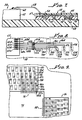
- FIG. 7 is a fragmentary sectional view showing portions of a chip and an LTCC module interconnected by a decal embodying principles of the present invention.
- FIG. 8 is a fragmentary plan view of the upper surface of the assembly of FIG. 7, illustrating certain patterns of electrical conductor routing.
- FIG. 9 is a plan view of a part of a chip and decal illustrating alternate patterns of electrically conductive trace routing.
- FIG. 10 is a fragmentary sectional view similar to FIG. 7 showing two decal layers interconnecting a chip with an LTCC module.
- FIG. 12 is a fragmentary plan view of a pattern of connections on the lower layer of decal of FIG. 10.
- FIG. 15 is a partial sectional view of the arrangement of FIG. 14.
- FIG. 1 Illustrated schematically in FIG. 1 is part of a multilayer low temperature co-fired ceramic interconnection module (LTCC) 10, having layers 10a-10f showing portions of connecting circuit traces 12 interconnected by vias 14, and having a surface mounted connecting pad 16.
- LTCC low temperature co-fired ceramic interconnection module
- a plurality of integrated circuit chips 18, 20, 22 and 24, each having a plurality of peripherally disposed contact pads, generally indicated at 18a, 20a, 22a and 24a, are mounted on a thin flexible decal 26 for connection to pads on the upper surface of top layer 10a of the LTCC module 10.
- Decal 26 is a thin flexible multilayer sheet of a substrate such as an adhesive clad dielectric (Kapton or other polyimide) carrying a pattern of electrically conductive circuit traces having primary and secondary interconnecting decal conductive pads formed thereon.
- the primary decal pad (FIG. 7) in one embodiment is formed by an end 55 of a decal circuit trace 46 and accessible through a hole 54 in the dielectric substrate 14 of the decal, whereas the secondary interconnecting decal pad 50 is formed as a projecting feature or bump extending from the opposite surface of the decal.
- the decal will cover the entire surface of the LTCC substrate, although, as shown in FIG. 7, a "window" or opening may be provided for one or more chips for improved heat transfer.
- Trace 46 has a first end 55 which will form a primary interconnecting decal pad of the trace 46 and a projecting feature or bump 50 which will form a secondary interconnecting decal pad of the connecting trace 46 (FIG. 5). Thereafter a dielectric core in the form of an adhesive clad dielectric such as a Kapton polyimide 52, predrilled with one or more holes 54, is laminated to the electrically deposited traces 46. Holes 54 are positioned to register with end portions of the interconnecting conductive trace 46. If deemed necessary or desirable, the interior of the projecting feature or bump 50 may be filled with an epoxy 56 prior to the application of the dielectric core 52 in order to stabilize and strengthen the bump.
- a dielectric core in the form of an adhesive clad dielectric such as a Kapton polyimide 52, predrilled with one or more holes 54, is laminated to the electrically deposited traces 46. Holes 54 are positioned to register with end portions of the interconnecting conductive trace 46. If deemed necessary or desirable, the interior of
- the decal comprises a thin flexible dielectric sheet bearing a pattern of many conductive traces such as trace 46, each of which has a primary decal pad at one end thereof (in this case formed by the end of trace 46 that is exposed in the substrate hole 54) and a secondary decal pad formed by the projecting feature defined by bump 50.
- the decal which has a total thickness not including the bump of about 2.0 mils is formed with a pattern of a number of electrically conductive traces 46 each having an interconnection pad at its opposite ends.
- the described additive electroplating process is but one of many known thin film lithographic processes by which the decal may be made.
- FIG. 7 illustrates a section of portions of the decal shown in FIG. 6 mounted on an LTCC module and configured and arranged to interconnect a pad 60 on a chip 62 to LTCC module 58.
- the decal substrate 52 includes a layer of Kapton polyimide 64 and a layer of adhesive 66 secured to the conductive trace 46.
- Connecting wire 68 is bonded to the chip pad 60 at one end and at the other end to the primary decal connecting pad 55 formed by the portion of conductor 46 that is exposed through substrate hole 54.
- the projecting feature or bump 50 of the decal which forms the secondary decal pad is positioned directly upon an LTCC connecting pad 70 formed on the upper surface of the LTCC module 58.
- FIG. 8 is a plan view of a small portion of the upper surface of the LTCC module 58 on which is mounted the chip 62 with chip pads 60a, 60b, 60c and 60d are shown, although it will be readily understood that the chip has more connecting pads positioned around its periphery.
- Chip pad 60a is connected by a bonded wire 68 to an end 55a of trace 46a at the other end of which is formed the projecting feature or depression 50a.
- the adhesive clad polyimide Kapton substrate of the decal is not shown in FIG. 8 for clarity of the drawings.
- Additional chip pads 60b, 60c and 60d are connected by wires 68b, 68c, 68d to primary decal pads 55b, 55c, 55d of decal conductive traces 46b, 46c and 46d which extend in the illustrated L-shaped configuration and have right angle end portions 47b, 47c and 47d respectively terminating in secondary decal pads or bumps 50b, 50c and 50d. These bumps are positioned over and electrically connected to additional LTCC module surface mounted pads 70b, 70c and 70d, respectively.
- the chip pads are close together, with these pads having a pitch of about 0.004 inches.
- the conductive traces 46 may have the same fine pitch as the chip pads.
- the LTCC pads 70 may be 0.008 inches on a side and spaced apart by 0.008 inches.
- the pattern of conductive traces 46 on the decal is provided with a suitable configuration such as the exemplary configuration illustrated in FIG. 8 that positions all of the secondary decal pads 50 of the decal conductors at positions registered with the coarse-pitch LTCC pads. In this manner, with a simple, inexpensive, independently formed flexible decal, the fine-pitch chip pads are readily connected electrically to the coarse pitch LTCC pads.
- Decals 80 and 86 may be integral parts of a single unitary decal that covers the entire LTCC substrate.
- FIG. 10 An alternative arrangement of interconnecting decals that minimizes use of surface area is shown in FIG. 10, which illustrates use of two layers of decals. Use of multiple layers of decals enables connections to be made in a manner that requires less surface area of the LTCC module, thereby allowing chips to be positioned closer to each other.
- parts corresponding to similar parts of FIGS. 7 - 9 are designated by similar reference numerals with a prefix 1 employed to designate elements of FIG. 10.
- a low temperature co-fired ceramic multilayer module 158 mounts a chip 162 having a pad 160 connected by a ball bonded wire 168 to a first decal layer 157 having an electrically conductive trace 146 and a primary decal pad 155 exposed through a hole 154 in the Kapton/adhesive substrate 152 that carries the conductive trace 146.
- a projecting feature or connecting bump 150 formed at the other end of trace 146 is connected by means of a conductive adhesive such as a silver epoxy 174, for example, to a portion 155a of the conductive trace 146a of a second similar decal layer 157a including an adhesive clad Kapton substrate 152a (including layers of Kapton and adhesive) having a hole 154a.
- the first decal layer 157 is secured to the second decal layer 157a by an interposed nonconductive adhesive layer 172.
- the bump 150a of conductor 146a of the second decal layer projects downwardly from the decal for connection to a contact pad 170 on the upper surface of LTCC 158. Bump 150a of the second decal layer is positioned closer to the chip 162 than is bump 150 of the first decal layer, thereby conserving horizontal area.
- the second decal layer 157a is secured to the LTCC module by a layer of nonconductive adhesive 172a.
- connections from the chip to the first decal layer extend outwardly of the chip periphery as shown in FIG. 11 but only for a relatively short distance.
- the first decal layer then connects to the second decal layer which redirects the connecting lines inwardly back toward the chip to provide relatively large spaces between the secondary connecting pads, e.g. bumps, of the second layer which are connected to the relatively coarse-pitch pads of the LTCC.
- the several bumps of the second decal layer are staggered horizontally (FIG. 12).
- chip density may be further enhanced by positioning the decal pads, such as bumps 150e and 150d (FIG. 12) of the second decal layer, directly beneath the chips, between the chip and LTCC module.
- Bump 255 rests on a chip contact pad 260 and is secured thereto by an electrically conductive adhesive or solder 261.
- the decal conductor 246 includes a second downwardly projecting feature or bump 250 resting on an LTCC contact pad 270 and electrically and mechanically connected therewith by means of solder or an electrically conductive adhesive 274.
- the decal is formed, as are all of the other decals described herein independently of the chip and independently of the LTCC. Preferably all decals are formed on the mandrel as described above. In the arrangement of FIG. 13 the pre-formed decal is first mounted to the chip which has been secured to the LTCC upper surface, and then the decal bumps 250 are connected to the LTCC pads.
- FIGS. 7 through 13 illustrate configurations that may be termed primarily types of "fan-out” arrangements in which connections are made from the chip to LTCC pads that are outside of the chip periphery.
- the types of fan-out shown in FIGS. 7 through 13 employ parallel lines, although the term “fan-out” is commonly used to denote lines that extend radially at different angles.
- Illustrated in FIGS. 14 and 15 is a chip-to-decal-to-LTCC module employing a "fan-in" arrangement wherein the contact pads along at least one side of a chip are connected to contact pads on the LTCC module that are within the perimeter of the chip and directly below the chip itself. This provides still further conservation of module surface and allows enhanced chip density.
- a chip 362 has its set of peripheral chip pads 360 connected by wires 368 to a decal 357 that is mounted on the upper surface of an LTCC module 358 having surface pads 370 thereon.
- each chip pad 360 is connected by a wire bonded lead 368 to a primary connecting pad 355 (FIG. 15) of the conductor 346 of the decal 357.
- Conductor 346 includes a secondary connecting decal pad in a form of a downwardly protruding bump 350 which is electrically connected to LTCC pad 370 at a point directly below the chip.
- the decal conductor 346 extends from the primary decal pad 355 inwardly toward and under the chip to its secondary decal pad or bump 350.
- the decal 357 includes a layer of adhesive 352a, a layer of polyimide 352b and a second double-adhesive clad polyimide layer 352c interposed between the chip and the decal for securely physically connecting the chip to the decal.
- Adhesive layer 352a connects the decal to the surface of the LTCC.
- a chip mounting arrangement termed a "flip chip” employs a chip having peripheral contact pads each formed with a protruding bump thereon. This enables the chip to be placed upside down on a substrate with the chip pad bumps in contact with pads formed on the substrate to directly connect the bumps of the chip pads to the substrate. This arrangement is effective in utilizing decreased area for chip mounting but requires specially prepared and therefore more expensive chips.
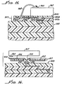
- the decal arrangement described above, with some modification, may be employed to effectively form a chip capable of flip chip mounting without forming the chip bumps when the chip is manufactured. Thus a chip not specially prepared can be used as a "flip chip". Illustrated in the exploded view of FIG. 16 is a chip 462 having a series of peripheral chip contact pads 460.
- the chip is mounted to an LTCC substrate module 458 by means of a decal 457 including a conductive trace 446 having a primary decal contact 455 coupled with a secondary decal contact or bump 450.
- the decal substrate includes a double-adhesive clad Kapton layer 452 that secures the decal both to the chip and to the LTCC module.
- the decal is positioned as shown in FIG. 16 directly below the chip with its primary contact pad 455 in electrical contact with the chip pad 460 and with its secondary contact pad or bump 450 connected with the LTCC pad 470 by means of an electrically conductive adhesive 474.
- the interconnecting circuit module shown in FIG.
- Module 16 as a multi-layer LTCC module 458, may be a substrate other than a thick film coarse-pitch device.
- Module 458, for example, may be a multilayered polyimide substrate formed by conventional thin film metalizing processes that enable provision of fine pitch connecting pads on the substrate.
- the contacting medium between the decal bump and the LTCC pad may be an electrically conductive z-axis conductive film, such as type 5303 made by 3M Company.
- Anisotropically conductive epoxy such as VriaxTM made by Polycon may also be employed for electrically connecting the decal bumps to the LTCC pads.
- the Polycon material for example, is a thin film containing a number of spaced conductive spheres. When the film is compressed, as between the decal bump and an LTCC pad, the electrically conductive spheres make contact through both sides of the film but do not contact one another.
- Still another mode of connecting the decal bumps to the LTCC is the use of a low melting temperature solder that can be applied locally as an alternative to the use of epoxy.
- Another arrangement for connection of the decal bumps to the LTCC pads is a non-conductive adhesive.
Landscapes
- Wire Bonding (AREA)
Applications Claiming Priority (2)
| Application Number | Priority Date | Filing Date | Title |
|---|---|---|---|
| US08/136,844 US5412539A (en) | 1993-10-18 | 1993-10-18 | Multichip module with a mandrel-produced interconnecting decal |
| US136844 | 1993-10-18 |
Publications (2)
| Publication Number | Publication Date |
|---|---|
| EP0649171A2 true EP0649171A2 (de) | 1995-04-19 |
| EP0649171A3 EP0649171A3 (de) | 1995-10-11 |
Family
ID=22474625
Family Applications (1)
| Application Number | Title | Priority Date | Filing Date |
|---|---|---|---|
| EP94307501A Withdrawn EP0649171A3 (de) | 1993-10-18 | 1994-10-13 | Mehrchipmodul mit einem mittels eines Zwischenträger produzierten Verdrahtungsfilm. |
Country Status (3)
| Country | Link |
|---|---|
| US (1) | US5412539A (de) |
| EP (1) | EP0649171A3 (de) |
| JP (1) | JP3069010B2 (de) |
Cited By (2)
| Publication number | Priority date | Publication date | Assignee | Title |
|---|---|---|---|---|
| EP1005086A3 (de) * | 1998-11-26 | 2001-01-03 | Shinko Electric Industries Co. Ltd. | Metallfolie mit Hockerkontakten, Schaltungssubstrat mit der Metallfolie, und Halbleitervorrichtung mit dem Schaltungssubstrat |
| EP1786034A3 (de) * | 2005-11-09 | 2008-07-09 | Semikron Elektronik GmbH & Co. KG Patentabteilung | Leistungshalbleitermodul |
Families Citing this family (28)
| Publication number | Priority date | Publication date | Assignee | Title |
|---|---|---|---|---|
| US5635761A (en) * | 1994-12-14 | 1997-06-03 | International Business Machines, Inc. | Internal resistor termination in multi-chip module environments |
| US5661647A (en) * | 1995-06-07 | 1997-08-26 | Hughes Electronics | Low temperature co-fired ceramic UHF/VHF power converters |
| US6232866B1 (en) | 1995-09-20 | 2001-05-15 | The United States Of America As Represented By The Administrator Of The National Aeronautics And Space Administration | Composite material switches |
| US6880245B2 (en) * | 1996-03-12 | 2005-04-19 | International Business Machines Corporation | Method for fabricating a structure for making contact with an IC device |
| US6061243A (en) * | 1997-11-06 | 2000-05-09 | Lockheed Martin Corporation | Modular and multifunctional structure |
| US6007669A (en) * | 1998-01-07 | 1999-12-28 | Packard Hughes Interconnect Company | Layer to layer interconnect |
| US6303988B1 (en) | 1998-04-22 | 2001-10-16 | Packard Hughes Interconnect Company | Wafer scale burn-in socket |
| US6510606B2 (en) * | 1998-06-15 | 2003-01-28 | Lockheed Martin Corporation | Multichip module |
| JP2000138104A (ja) * | 1998-08-26 | 2000-05-16 | Yazaki Corp | 回路保護素子の検査構造 |
| US6627998B1 (en) * | 2000-07-27 | 2003-09-30 | International Business Machines Corporation | Wafer scale thin film package |
| US6600224B1 (en) * | 2000-10-31 | 2003-07-29 | International Business Machines Corporation | Thin film attachment to laminate using a dendritic interconnection |
| US7200405B2 (en) * | 2003-11-18 | 2007-04-03 | Interdigital Technology Corporation | Method and system for providing channel assignment information used to support uplink and downlink channels |
| US7494557B1 (en) | 2004-01-30 | 2009-02-24 | Sandia Corporation | Method of using sacrificial materials for fabricating internal cavities in laminated dielectric structures |
| CA2490676A1 (en) * | 2004-12-16 | 2006-06-16 | Ibm Canada Limited - Ibm Canada Limitee | Releasably mountable electronics component |
| US7901989B2 (en) | 2006-10-10 | 2011-03-08 | Tessera, Inc. | Reconstituted wafer level stacking |
| US8513789B2 (en) * | 2006-10-10 | 2013-08-20 | Tessera, Inc. | Edge connect wafer level stacking with leads extending along edges |
| US7829438B2 (en) | 2006-10-10 | 2010-11-09 | Tessera, Inc. | Edge connect wafer level stacking |
| US7759166B2 (en) * | 2006-10-17 | 2010-07-20 | Tessera, Inc. | Microelectronic packages fabricated at the wafer level and methods therefor |
| US7952195B2 (en) * | 2006-12-28 | 2011-05-31 | Tessera, Inc. | Stacked packages with bridging traces |
| CN101809739B (zh) * | 2007-07-27 | 2014-08-20 | 泰塞拉公司 | 具有后应用的衬垫延长部分的重构晶片堆封装 |
| WO2009020572A2 (en) | 2007-08-03 | 2009-02-12 | Tessera Technologies Hungary Kft. | Stack packages using reconstituted wafers |
| US8043895B2 (en) * | 2007-08-09 | 2011-10-25 | Tessera, Inc. | Method of fabricating stacked assembly including plurality of stacked microelectronic elements |
| JP5048420B2 (ja) * | 2007-08-17 | 2012-10-17 | 新光電気工業株式会社 | 半導体装置及びその製造方法 |
| JP5639052B2 (ja) * | 2008-06-16 | 2014-12-10 | テッセラ,インコーポレイテッド | ウェハレベルでの縁部の積重ね |
| KR101022912B1 (ko) * | 2008-11-28 | 2011-03-17 | 삼성전기주식회사 | 금속범프를 갖는 인쇄회로기판 및 그 제조방법 |
| US8466542B2 (en) * | 2009-03-13 | 2013-06-18 | Tessera, Inc. | Stacked microelectronic assemblies having vias extending through bond pads |
| GB0918221D0 (en) * | 2009-10-16 | 2009-12-02 | Cambridge Silicon Radio Ltd | Inductor structure |
| US10840056B2 (en) * | 2017-02-03 | 2020-11-17 | Kla Corporation | Multi-column scanning electron microscopy system |
Family Cites Families (9)
| Publication number | Priority date | Publication date | Assignee | Title |
|---|---|---|---|---|
| US4549200A (en) * | 1982-07-08 | 1985-10-22 | International Business Machines Corporation | Repairable multi-level overlay system for semiconductor device |
| US5061988A (en) * | 1990-07-30 | 1991-10-29 | Mcdonnell Douglas Corporation | Integrated circuit chip interconnect |
| DE4030055A1 (de) * | 1990-09-22 | 1992-03-26 | Bosch Gmbh Robert | Verfahren zum herstellen einer schaltung |
| US5148265A (en) * | 1990-09-24 | 1992-09-15 | Ist Associates, Inc. | Semiconductor chip assemblies with fan-in leads |
| US5132879A (en) * | 1990-10-01 | 1992-07-21 | Hewlett-Packard Company | Secondary board for mounting of components having differing bonding requirements |
| US5245750A (en) * | 1992-02-28 | 1993-09-21 | Hughes Aircraft Company | Method of connecting a spaced ic chip to a conductor and the article thereby obtained |
| US5245135A (en) * | 1992-04-20 | 1993-09-14 | Hughes Aircraft Company | Stackable high density interconnection mechanism (SHIM) |
| US5313366A (en) * | 1992-08-12 | 1994-05-17 | International Business Machines Corporation | Direct chip attach module (DCAM) |
| US5280413A (en) * | 1992-09-17 | 1994-01-18 | Ceridian Corporation | Hermetically sealed circuit modules having conductive cap anchors |
-
1993
- 1993-10-18 US US08/136,844 patent/US5412539A/en not_active Expired - Lifetime
-
1994
- 1994-10-13 EP EP94307501A patent/EP0649171A3/de not_active Withdrawn
- 1994-10-18 JP JP6251993A patent/JP3069010B2/ja not_active Expired - Lifetime
Cited By (3)
| Publication number | Priority date | Publication date | Assignee | Title |
|---|---|---|---|---|
| EP1005086A3 (de) * | 1998-11-26 | 2001-01-03 | Shinko Electric Industries Co. Ltd. | Metallfolie mit Hockerkontakten, Schaltungssubstrat mit der Metallfolie, und Halbleitervorrichtung mit dem Schaltungssubstrat |
| US6420664B1 (en) | 1998-11-26 | 2002-07-16 | Shinko Electric Industries, Co., Ltd. | Metal foil having bumps, circuit substrate having the metal foil, and semiconductor device having the circuit substrate |
| EP1786034A3 (de) * | 2005-11-09 | 2008-07-09 | Semikron Elektronik GmbH & Co. KG Patentabteilung | Leistungshalbleitermodul |
Also Published As
| Publication number | Publication date |
|---|---|
| EP0649171A3 (de) | 1995-10-11 |
| JP3069010B2 (ja) | 2000-07-24 |
| US5412539A (en) | 1995-05-02 |
| JPH07201902A (ja) | 1995-08-04 |
Similar Documents
| Publication | Publication Date | Title |
|---|---|---|
| US5412539A (en) | Multichip module with a mandrel-produced interconnecting decal | |
| EP0567814B1 (de) | Leiterplatte zur Montage von Halbleitern und sonstigen elektronischen Bauelementen | |
| US5432677A (en) | Multi-chip integrated circuit module | |
| US6400573B1 (en) | Multi-chip integrated circuit module | |
| US7723838B2 (en) | Package structure having semiconductor device embedded within wiring board | |
| US6849945B2 (en) | Multi-layered semiconductor device and method for producing the same | |
| JP3813402B2 (ja) | 半導体装置の製造方法 | |
| US7501696B2 (en) | Semiconductor chip-embedded substrate and method of manufacturing same | |
| US7506437B2 (en) | Printed circuit board having chip package mounted thereon and method of fabricating same | |
| KR950012658B1 (ko) | 반도체 칩 실장방법 및 기판 구조체 | |
| US5719749A (en) | Printed circuit assembly with fine pitch flexible printed circuit overlay mounted to printed circuit board | |
| US6256877B1 (en) | Method for transforming a substrate with edge contacts into a ball grid array | |
| KR100537972B1 (ko) | 집적 회로 패키지용 칩 스케일 볼 그리드 어레이 | |
| KR100268742B1 (ko) | 고밀도 인쇄회로 기판에 패드를 부착하는 방법,다중층 인쇄회로 기판의 형성 방법 및 다중층 회로기판 | |
| EP1005086B1 (de) | Metallfolie mit Hockerkontakten, Schaltungssubstrat mit der Metallfolie, und Halbleitervorrichtung mit dem Schaltungssubstrat | |
| US6495912B1 (en) | Structure of ceramic package with integrated passive devices | |
| JP2768650B2 (ja) | ソルダーボールの装着溝を有する印刷回路基板とこれを使用したボールグリッドアレイパッケージ | |
| US5920123A (en) | Multichip module assembly having via contacts and method of making the same | |
| EP0632685A2 (de) | Elastische Schaltplatinenanordnung mit gemeinsamer Wärmeabfuhr sowie Herstellungsverfahren hierfür | |
| EP0377932A2 (de) | Baugruppe von integrierten Halbleiterschaltungen | |
| US20040135243A1 (en) | Semiconductor device, its manufacturing method and electronic device | |
| JP2003522401A (ja) | 積層型集積回路パッケージ | |
| JPH11312756A (ja) | 半導体装置 | |
| US4933810A (en) | Integrated circuit interconnector | |
| KR101489798B1 (ko) | 배선 기판 |
Legal Events
| Date | Code | Title | Description |
|---|---|---|---|
| PUAI | Public reference made under article 153(3) epc to a published international application that has entered the european phase |
Free format text: ORIGINAL CODE: 0009012 |
|
| AK | Designated contracting states |
Kind code of ref document: A2 Designated state(s): DE FR GB |
|
| PUAL | Search report despatched |
Free format text: ORIGINAL CODE: 0009013 |
|
| AK | Designated contracting states |
Kind code of ref document: A3 Designated state(s): DE FR GB |
|
| 17P | Request for examination filed |
Effective date: 19960314 |
|
| STAA | Information on the status of an ep patent application or granted ep patent |
Free format text: STATUS: THE APPLICATION HAS BEEN WITHDRAWN |
|
| 18W | Application withdrawn |
Withdrawal date: 19970812 |