EP0650065A2 - Adaptateur à vide - Google Patents
Adaptateur à vide Download PDFInfo
- Publication number
- EP0650065A2 EP0650065A2 EP94116483A EP94116483A EP0650065A2 EP 0650065 A2 EP0650065 A2 EP 0650065A2 EP 94116483 A EP94116483 A EP 94116483A EP 94116483 A EP94116483 A EP 94116483A EP 0650065 A2 EP0650065 A2 EP 0650065A2
- Authority
- EP
- European Patent Office
- Prior art keywords
- vacuum
- plate
- contact carrier
- carrier plate
- guide
- Prior art date
- Legal status (The legal status is an assumption and is not a legal conclusion. Google has not performed a legal analysis and makes no representation as to the accuracy of the status listed.)
- Ceased
Links
- 230000000712 assembly Effects 0.000 claims description 7
- 238000000429 assembly Methods 0.000 claims description 7
- VVQNEPGJFQJSBK-UHFFFAOYSA-N Methyl methacrylate Chemical compound COC(=O)C(C)=C VVQNEPGJFQJSBK-UHFFFAOYSA-N 0.000 claims description 4
- 229920005372 Plexiglas® Polymers 0.000 claims description 4
- 238000000034 method Methods 0.000 claims description 3
- 239000012780 transparent material Substances 0.000 claims description 2
- 230000002093 peripheral effect Effects 0.000 claims 1
- 230000006978 adaptation Effects 0.000 abstract 1
- 238000010276 construction Methods 0.000 description 2
- 241000283973 Oryctolagus cuniculus Species 0.000 description 1
- 238000001816 cooling Methods 0.000 description 1
- 238000009429 electrical wiring Methods 0.000 description 1
- 239000006260 foam Substances 0.000 description 1
- 230000003993 interaction Effects 0.000 description 1
- 238000007789 sealing Methods 0.000 description 1
- 230000008054 signal transmission Effects 0.000 description 1
Images

Classifications
-
- G—PHYSICS
- G01—MEASURING; TESTING
- G01R—MEASURING ELECTRIC VARIABLES; MEASURING MAGNETIC VARIABLES
- G01R1/00—Details of instruments or arrangements of the types included in groups G01R5/00 - G01R13/00 and G01R31/00
- G01R1/02—General constructional details
- G01R1/06—Measuring leads; Measuring probes
- G01R1/067—Measuring probes
- G01R1/073—Multiple probes
- G01R1/07307—Multiple probes with individual probe elements, e.g. needles, cantilever beams or bump contacts, fixed in relation to each other, e.g. bed of nails fixture or probe card
- G01R1/07314—Multiple probes with individual probe elements, e.g. needles, cantilever beams or bump contacts, fixed in relation to each other, e.g. bed of nails fixture or probe card the body of the probe being perpendicular to test object, e.g. bed of nails or probe with bump contacts on a rigid support
- G01R1/07328—Multiple probes with individual probe elements, e.g. needles, cantilever beams or bump contacts, fixed in relation to each other, e.g. bed of nails fixture or probe card the body of the probe being perpendicular to test object, e.g. bed of nails or probe with bump contacts on a rigid support for testing printed circuit boards
Definitions
- the invention relates to a vacuum adapter for contacting electronic assemblies to be tested with a test device, the bottom of which consists of an interface plate provided with grid holes, which is surrounded by a frame that contains first vacuum slots, on which a first contact carrier plate with second vacuum slots rests, both contains contact pins protruding into the grid holes of the interface plate, as well as upward and downward protruding test needles, which are electrically connected to the connection contact pins, this first contact carrier plate, together with a pressure plate and a first seal rotating between the two at the periphery, forming a first vacuum chamber, whereby the first and second vacuum slots form a feed channel to the vacuum chamber, and the electronic flat modules to be tested can be placed on the pressure plate via the second seal.
- a one-sided contacting vacuum test adapter is known from the HP 3070 Test Fixture Product Catalog, April 1989, pages 2 and 3. It consists of a substructure with an interface plate of a first contact carrier plate, a pressure plate and the seal in between. These three components form a vacuum chamber which, when a vacuum is generated, presses the electronics module on the pressure plate against the adapter needles of the first contact carrier plate, whereby contact is made with the test points on the electronics module, e.g. Catalog 1992, page 12, test adapters, accessories, services from Ingun.
- Double-sided vacuum adapters are also known. So far, however, these can only be used for a relatively small area and do not have a sufficiently precise guidance system to achieve the required accuracy. The construction is usually carried out with a full hood, so that additional hold-down devices are required. In addition, there is no possibility of cooling the test specimen and there is no access to the module for debugging the test program. Due to their structure, they are severely limited with regard to the maximum test size and minimum test point size.
- the object of the present invention is to provide a double-sided vacuum adapter with a high degree of accuracy in the contacting of the adapter needles with the test points of the electronic assembly.
- the vacuum test adapter is designed in such a way that third respective second vacuum chambers are arranged on the end faces of the pressure plate, which, together with a second contact carrier plate, have both test needles and connecting contact pins, which are connected to one another via wiring, and are covered with a cover plate, and that the pressure plate contains third vacuum slots which are congruent with the second vacuum slots of the lower contact carrier plate.
- the second contact carrier plate can advantageously be fastened in a hinged frame.
- the cover plate is expediently made of transparent material, such as plexiglass.
- a guide unit is attached to the first contact carrier plate at its four corners, which in each case consists of a guide pin which is guided through a bushing located in the pressure plate and at its upper end one secured with a hand screw Contains guide sleeve with an outer cone, which is pressed up by means of a pressure spring supported on the pressure plate, and that a guide flange is fastened in alignment with the guide pin in the second contact carrier plate, which engages with the inner cone of the outer cone of the guide pins when closed.
- a vacuum-tight guide cover can be arranged on the second contact carrier plate, which contains a recess into which the guide pin moves after the closing process.
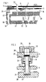
- the one-sided adapter according to FIG. 1 consists of the interface plate 22, the all-round frame 19 with the first vacuum slots 34, the first contact carrier plate 20 with the second vacuum slots 17 placed on this frame, and the connection contact pins 31 arranged on it, which fit into the grid holes 33 in FIG Interface plate 22 protrude and the test needles 7, which are electrically connected on their underside to the terminal contact pins 31.
- the test needles 7 protrude through the pressure plate 9, which is placed on a first seal 21 running all around on the first contact carrier plate 20.
- the first Contact carrier plate 20 forms, together with the first seal 21 and the pressure plate 9, the first vacuum chamber 15 and the first slots 34 and the second slots 17 together form the channel connecting the first vacuum chamber 15 to the external environment, via which the vacuum can be established.
- the electronic flat module 6 to be tested then lies on a second seal 14, which also runs all around on the pressure plate surface. If a vacuum is generated in the first vacuum chamber 15, the electronic flat module 6 is contacted with the test needles 7 on the pads provided and the test of the electronic flat module 6 can now take place via the test device connected to the connection contact pins 31 of the interface plate 22.
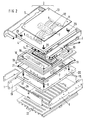
- the exploded drawing according to FIG. 2 again shows the interface plate 22, as well as the all-round frame 19 with the first vacuum slots 34, and the first contact carrier plate 20 with the test needles 7 and the guide units 8.
- the first seal 21 which has a V-shaped profile, can be seen.
- the second vacuum slots 17 can also be seen on the first contact carrier plate.
- the upper adapter unit 3 for double-sided operation now begins, ie the electronic assemblies 9 can be contacted with the test needles 7 both from below and from above.
- the construction begins with the lower frame strips 1, which are screwed to the left and right of the frame 19.
- frame strips 1 connect by means of joint rods 2 the upper adapter unit 3, consisting of the elements: second contact carrier plate 4 with the electrical wiring 12, upper frame 5 for opening, as well as the elements permanently attached to it, such as the plexiglass plate 13 with the frame 5 upper adapter unit 3 or the second contact carrier plate 4 located therein after inserting the electronic assembly 6 is congruent with the test needles 7 contacting from below, a guide unit 8 described in more detail in FIG. 3 must catch and guide the second contact carrier plate 4.
- the vacuum actuation is made possible by two built-in second vacuum chambers 16, which are formed between the pressure plate 9 and the second contact carrier plate 4 after the upper adapter unit 3 has been closed.
- the vacuum connection of the individual second vacuum chambers takes place via the first vacuum slots 34, the second vacuum slots 17 and the third vacuum slots 18 located in the pressure plate 9.
- the third seals 10 between the pressure plate 9 and the second contact carrier plate 4, which delimit the second vacuum chambers 16, are laid so that the interface needles 11 are in a vacuum for signal transmission. They are arranged on the front and rear front of the pressure plate 9.
- the electronic flat module 6 is placed on the pressure plate 9 via the second module seal 14, which is arranged between the two second vacuum chambers 16.
- the function of the double-sided vacuum-operated needle adapter is as follows: After inserting the electronic flat module 6 into the second seal 14, the upper adapter unit 3 is closed onto the electronic flat module 6. The second seal 14 is glued to the pressure plate 9. Now vacuum is applied. Due to the negative pressure acting in the first and second vacuum chambers 15, 16, the entire arrangement is compressed like a sandwich. The upper adapter unit 3 moves towards the electronic flat module 6. The flat module 6 is contacted by the upper test needles 7, which are embedded in the second contact carrier plate 4. On the other hand, the electronic flat module 6 fixed on the pressure plate 9 moves toward the first contact carrier plate 20. The electronics assembly 6 is contacted by the lower test needles 7 embedded in the first contact carrier plate 20. The electrical test of the printed circuit board can now begin.
- the guide unit 8 is constructed as shown in FIG. 3.
- the pressure plate 9 and the second contact carrier plate 4 are threaded onto the guide pin 23, screwed into the first contact carrier plate 20.
- guide bushes 24 are inserted into the pressure plate 9.
- the interface when opening and closing the upper adapter unit 3 is formed by the guide sleeve 25 with the outer cone and the guide flange 26 with the inner cone. So that the guide sleeve 25 with the outer cone also catches and centers the guide flange 26 fastened to the second contact carrier plate 4 during the closing process, it is held upward by the counter pressure spring 27. This arrangement is secured by the hand screw 28.
- the conical shape on both guide elements 25, 26 permits greater misalignments (catch tolerances) when the upper adapter unit 3 or the upper contact carrier plate 4 is closed.
- the guide cover 29 with built-in sealing ring 30 closes the system in a vacuum-tight manner.
- the upper adapter unit 3 is sucked in because of the two second vacuum chambers 16, which are each located next to the flat module 6 and between the pressure plate 9 and the second contact plate 4.
- the arrangement of the second seals 10 and the possibility of placing interface adapters 11 within the vacuum chambers 16 are advantageous.
- the interface needles 11 transmit the test signals tapped from above to the test system.
- the second seals 10 can be rectangular foam profile seals.
- FIG. 4 The interaction of the upper adapter unit 3 with the lower adapter part is shown in FIG. 4 in different positions.
- the upper adapter unit In the first position, the upper adapter unit is fully opened. One recognizes the upper frame 5, as well as the plexiglass cover 13 and the joint rods 2.
- the second position a state is shown in which the guide elements 25 and 26 have already been shifted into one another.
- the third position is then indicated to the right, in which the upper adapter unit is pivoted in completely and the test state is reached.
- the second and third positions are also shown in the area of the test needles 7 and the interface needles 11 further to the right in the figure.
Landscapes
- Physics & Mathematics (AREA)
- General Physics & Mathematics (AREA)
- Testing Of Individual Semiconductor Devices (AREA)
- Tests Of Electronic Circuits (AREA)
Applications Claiming Priority (2)
| Application Number | Priority Date | Filing Date | Title |
|---|---|---|---|
| DE19934335841 DE4335841C1 (de) | 1993-10-20 | 1993-10-20 | Vakuumadapter |
| DE4335841 | 1993-10-20 |
Publications (2)
| Publication Number | Publication Date |
|---|---|
| EP0650065A2 true EP0650065A2 (fr) | 1995-04-26 |
| EP0650065A3 EP0650065A3 (fr) | 1996-07-03 |
Family
ID=6500620
Family Applications (1)
| Application Number | Title | Priority Date | Filing Date |
|---|---|---|---|
| EP94116483A Ceased EP0650065A3 (fr) | 1993-10-20 | 1994-10-19 | Adaptateur à vide. |
Country Status (2)
| Country | Link |
|---|---|
| EP (1) | EP0650065A3 (fr) |
| DE (1) | DE4335841C1 (fr) |
Cited By (3)
| Publication number | Priority date | Publication date | Assignee | Title |
|---|---|---|---|---|
| EP0840131A3 (fr) * | 1996-10-29 | 1999-06-09 | Hewlett-Packard Company | Dispositif de test de circuits imprimés avec guidage des pointes de test |
| EP0840130A3 (fr) * | 1996-10-29 | 1999-06-09 | Hewlett-Packard Company | Dispositif de test hybride pour des régions à accès standards ou limités |
| US6784675B2 (en) | 2002-06-25 | 2004-08-31 | Agilent Technologies, Inc. | Wireless test fixture adapter for printed circuit assembly tester |
Families Citing this family (1)
| Publication number | Priority date | Publication date | Assignee | Title |
|---|---|---|---|---|
| DE19857979A1 (de) * | 1998-12-16 | 2000-06-21 | Aurion Anlagentechnik Gmbh | Vakuumkammer |
Family Cites Families (8)
| Publication number | Priority date | Publication date | Assignee | Title |
|---|---|---|---|---|
| GB2172150B (en) * | 1985-03-05 | 1988-06-08 | Marconi Instruments Ltd | Probe arrays for testing circuit boards |
| GB8622878D0 (en) * | 1986-09-23 | 1986-10-29 | Marconi Instruments Ltd | Electrical interface arrangement |
| DE3637406C1 (en) * | 1986-11-03 | 1988-05-05 | Genrad Gmbh | Test device for circuit boards |
| DE3710093A1 (de) * | 1987-03-27 | 1988-10-06 | Ptr Messtechnik Gmbh Messmitte | Leiterplattenpruefgeraet fuer beidseitig smd-bestueckte leiterplatten |
| DE3841087A1 (de) * | 1988-12-07 | 1990-06-21 | Franz Mothes | Vacuum - adapter mit balgdichtung, zur kontaktierung von bestueckten platinen in herkoemmlicher und in smd-bauweise |
| US4993136A (en) * | 1989-06-19 | 1991-02-19 | Hewlett-Packard Company | Method of converting a vacuum test fixture on a board testing apparatus to a mechanical test fixture |
| DE4100014C2 (de) * | 1991-01-02 | 1995-05-11 | Siemens Nixdorf Inf Syst | Prüfvorrichtung zum Prüfen von Leiterplatten |
| DE69229389T2 (de) * | 1992-02-25 | 1999-10-07 | Hewlett-Packard Co., Palo Alto | Testsystem für Schaltkreise |
-
1993
- 1993-10-20 DE DE19934335841 patent/DE4335841C1/de not_active Expired - Fee Related
-
1994
- 1994-10-19 EP EP94116483A patent/EP0650065A3/fr not_active Ceased
Cited By (4)
| Publication number | Priority date | Publication date | Assignee | Title |
|---|---|---|---|---|
| EP0840131A3 (fr) * | 1996-10-29 | 1999-06-09 | Hewlett-Packard Company | Dispositif de test de circuits imprimés avec guidage des pointes de test |
| EP0840130A3 (fr) * | 1996-10-29 | 1999-06-09 | Hewlett-Packard Company | Dispositif de test hybride pour des régions à accès standards ou limités |
| EP1512978A3 (fr) * | 1996-10-29 | 2005-06-15 | Agilent Technologies Inc. (a Delaware Corporation) | Dispositif de test de circuits imprimés avec guidage des pointes de test |
| US6784675B2 (en) | 2002-06-25 | 2004-08-31 | Agilent Technologies, Inc. | Wireless test fixture adapter for printed circuit assembly tester |
Also Published As
| Publication number | Publication date |
|---|---|
| DE4335841C1 (de) | 1995-06-01 |
| EP0650065A3 (fr) | 1996-07-03 |
Similar Documents
| Publication | Publication Date | Title |
|---|---|---|
| DE3240916C2 (de) | Vorrichtung zum Prüfen von elektrischen Leiterplatten | |
| DE2608430C3 (de) | Halterung für programmierbare Sonden zum Anschluß an ein in einer elektrischen Prüfung befindliches Bauteil | |
| DE2707900C3 (de) | Universal-Adaptiervorrichtung für Geräte zur elektrischen Prüfung unterschiedlicher gedruckter Schaltungen | |
| DE2617190A1 (de) | Einrichtungen zum pruefen von elektrischen vorrichtungen | |
| DE3716240A1 (de) | Pruefadapter, insbesondere fuer eine integrierte schaltung | |
| DE10320132A1 (de) | Verbinderkabel und Verfahren zum Sondieren von vakuumabdichtbaren elektronischen Knoten einer elektrischen Testvorrichtung | |
| EP0224471B1 (fr) | Dispositif pour tester des cartes de circuits imprimés | |
| DE4335841C1 (de) | Vakuumadapter | |
| EP0217193B1 (fr) | Dispositif de support et de test pour des éléments électroniques montés sur des supports plats | |
| DE3529207C1 (en) | Test device for electrical circuit boards | |
| EP0772048B1 (fr) | Dispositif de test de circuits imprimés et/ou des circuits plats | |
| DE3402845A1 (de) | Baugruppeneinschub | |
| DE3113375A1 (de) | Adaptereinrichtung und verfahren zur elektrischen verdrahtungspruefung von unbestueckten leiterplatten | |
| DE3040340A1 (de) | Pruefaufnahme fuer plattenfoermige baugruppen | |
| DE3710093A1 (de) | Leiterplattenpruefgeraet fuer beidseitig smd-bestueckte leiterplatten | |
| DE4338135C2 (de) | Adaptereinrichtung zum Anschluß von Kontaktpunkten eines Prüflings an eine Prüfeinrichtung | |
| DE3148285A1 (de) | Pruefadapter zum ankontaktieren von zu pruefenden elektronik-flachbaugruppen (leiterplatten) an ein universal-pruefgeraet | |
| DE3212403C2 (de) | Adaptereinrichtung zur Herstellung einer lösbaren elektrischen Verbindung zwischen Kontaktelementen einer Verdrahtungsplatte und zugeordneten Kontaktelementen einer Flachbaugruppe | |
| DE3144535A1 (de) | Anzeigeeinrichtung mit fluessigkristallanzeige | |
| EP1088238B1 (fr) | Socle adaptateur destine a recevoir des objets electroniques a tester | |
| DE19814312C2 (de) | Vorrichtung zum automatischen Testen von Baugruppen oder Bauateilen | |
| DE2607253C3 (de) | Hohlleiterkupplung | |
| DE3610286A1 (de) | Vorrichtung zum pruefen elektronischer apparaturen | |
| EP0880706A1 (fr) | Montage pour le controle de structures a semiconducteur | |
| DE19852442C2 (de) | Vorrichtung zum Testen oberflächenmontierbarer integrierter Schaltungen |
Legal Events
| Date | Code | Title | Description |
|---|---|---|---|
| PUAI | Public reference made under article 153(3) epc to a published international application that has entered the european phase |
Free format text: ORIGINAL CODE: 0009012 |
|
| AK | Designated contracting states |
Kind code of ref document: A2 Designated state(s): AT BE CH DE FR GB IT LI NL |
|
| PUAL | Search report despatched |
Free format text: ORIGINAL CODE: 0009013 |
|
| AK | Designated contracting states |
Kind code of ref document: A3 Designated state(s): AT BE CH DE FR GB IT LI NL |
|
| 17P | Request for examination filed |
Effective date: 19961219 |
|
| GRAG | Despatch of communication of intention to grant |
Free format text: ORIGINAL CODE: EPIDOS AGRA |
|
| 17Q | First examination report despatched |
Effective date: 20010530 |
|
| STAA | Information on the status of an ep patent application or granted ep patent |
Free format text: STATUS: THE APPLICATION HAS BEEN REFUSED |
|
| 18R | Application refused |
Effective date: 20020221 |