EP0650193A2 - Semiconductor device and method for manufacturing the same - Google Patents
Semiconductor device and method for manufacturing the same Download PDFInfo
- Publication number
- EP0650193A2 EP0650193A2 EP94115966A EP94115966A EP0650193A2 EP 0650193 A2 EP0650193 A2 EP 0650193A2 EP 94115966 A EP94115966 A EP 94115966A EP 94115966 A EP94115966 A EP 94115966A EP 0650193 A2 EP0650193 A2 EP 0650193A2
- Authority
- EP
- European Patent Office
- Prior art keywords
- substrate
- semiconductor device
- heat dissipation
- dissipation plate
- pattern member
- Prior art date
- Legal status (The legal status is an assumption and is not a legal conclusion. Google has not performed a legal analysis and makes no representation as to the accuracy of the status listed.)
- Ceased
Links
Images


Classifications
-
- H—ELECTRICITY
- H10—SEMICONDUCTOR DEVICES; ELECTRIC SOLID-STATE DEVICES NOT OTHERWISE PROVIDED FOR
- H10W—GENERIC PACKAGES, INTERCONNECTIONS, CONNECTORS OR OTHER CONSTRUCTIONAL DETAILS OF DEVICES COVERED BY CLASS H10
- H10W74/00—Encapsulations, e.g. protective coatings
- H10W74/10—Encapsulations, e.g. protective coatings characterised by their shape or disposition
- H10W74/111—Encapsulations, e.g. protective coatings characterised by their shape or disposition the semiconductor body being completely enclosed
- H10W74/114—Encapsulations, e.g. protective coatings characterised by their shape or disposition the semiconductor body being completely enclosed by a substrate and the encapsulations
-
- H—ELECTRICITY
- H10—SEMICONDUCTOR DEVICES; ELECTRIC SOLID-STATE DEVICES NOT OTHERWISE PROVIDED FOR
- H10W—GENERIC PACKAGES, INTERCONNECTIONS, CONNECTORS OR OTHER CONSTRUCTIONAL DETAILS OF DEVICES COVERED BY CLASS H10
- H10W70/00—Package substrates; Interposers; Redistribution layers [RDL]
- H10W70/40—Leadframes
- H10W70/456—Materials
-
- H—ELECTRICITY
- H10—SEMICONDUCTOR DEVICES; ELECTRIC SOLID-STATE DEVICES NOT OTHERWISE PROVIDED FOR
- H10W—GENERIC PACKAGES, INTERCONNECTIONS, CONNECTORS OR OTHER CONSTRUCTIONAL DETAILS OF DEVICES COVERED BY CLASS H10
- H10W40/00—Arrangements for thermal protection or thermal control
- H10W40/70—Fillings or auxiliary members in containers or in encapsulations for thermal protection or control
- H10W40/77—Auxiliary members characterised by their shape
- H10W40/778—Auxiliary members characterised by their shape in encapsulations
-
- H—ELECTRICITY
- H10—SEMICONDUCTOR DEVICES; ELECTRIC SOLID-STATE DEVICES NOT OTHERWISE PROVIDED FOR
- H10W—GENERIC PACKAGES, INTERCONNECTIONS, CONNECTORS OR OTHER CONSTRUCTIONAL DETAILS OF DEVICES COVERED BY CLASS H10
- H10W70/00—Package substrates; Interposers; Redistribution layers [RDL]
- H10W70/40—Leadframes
- H10W70/421—Shapes or dispositions
-
- H—ELECTRICITY
- H10—SEMICONDUCTOR DEVICES; ELECTRIC SOLID-STATE DEVICES NOT OTHERWISE PROVIDED FOR
- H10W—GENERIC PACKAGES, INTERCONNECTIONS, CONNECTORS OR OTHER CONSTRUCTIONAL DETAILS OF DEVICES COVERED BY CLASS H10
- H10W76/00—Containers; Fillings or auxiliary members therefor; Seals
- H10W76/40—Fillings or auxiliary members in containers, e.g. centering rings
-
- H—ELECTRICITY
- H10—SEMICONDUCTOR DEVICES; ELECTRIC SOLID-STATE DEVICES NOT OTHERWISE PROVIDED FOR
- H10W—GENERIC PACKAGES, INTERCONNECTIONS, CONNECTORS OR OTHER CONSTRUCTIONAL DETAILS OF DEVICES COVERED BY CLASS H10
- H10W76/00—Containers; Fillings or auxiliary members therefor; Seals
- H10W76/60—Seals
-
- H—ELECTRICITY
- H10—SEMICONDUCTOR DEVICES; ELECTRIC SOLID-STATE DEVICES NOT OTHERWISE PROVIDED FOR
- H10W—GENERIC PACKAGES, INTERCONNECTIONS, CONNECTORS OR OTHER CONSTRUCTIONAL DETAILS OF DEVICES COVERED BY CLASS H10
- H10W90/00—Package configurations
- H10W90/811—Multiple chips on leadframes
-
- H—ELECTRICITY
- H10—SEMICONDUCTOR DEVICES; ELECTRIC SOLID-STATE DEVICES NOT OTHERWISE PROVIDED FOR
- H10W—GENERIC PACKAGES, INTERCONNECTIONS, CONNECTORS OR OTHER CONSTRUCTIONAL DETAILS OF DEVICES COVERED BY CLASS H10
- H10W72/00—Interconnections or connectors in packages
- H10W72/50—Bond wires
-
- H—ELECTRICITY
- H10—SEMICONDUCTOR DEVICES; ELECTRIC SOLID-STATE DEVICES NOT OTHERWISE PROVIDED FOR
- H10W—GENERIC PACKAGES, INTERCONNECTIONS, CONNECTORS OR OTHER CONSTRUCTIONAL DETAILS OF DEVICES COVERED BY CLASS H10
- H10W72/00—Interconnections or connectors in packages
- H10W72/50—Bond wires
- H10W72/531—Shapes of wire connectors
- H10W72/5363—Shapes of wire connectors the connected ends being wedge-shaped
-
- H—ELECTRICITY
- H10—SEMICONDUCTOR DEVICES; ELECTRIC SOLID-STATE DEVICES NOT OTHERWISE PROVIDED FOR
- H10W—GENERIC PACKAGES, INTERCONNECTIONS, CONNECTORS OR OTHER CONSTRUCTIONAL DETAILS OF DEVICES COVERED BY CLASS H10
- H10W72/00—Interconnections or connectors in packages
- H10W72/50—Bond wires
- H10W72/551—Materials of bond wires
- H10W72/552—Materials of bond wires comprising metals or metalloids, e.g. silver
- H10W72/5522—Materials of bond wires comprising metals or metalloids, e.g. silver comprising gold [Au]
-
- H—ELECTRICITY
- H10—SEMICONDUCTOR DEVICES; ELECTRIC SOLID-STATE DEVICES NOT OTHERWISE PROVIDED FOR
- H10W—GENERIC PACKAGES, INTERCONNECTIONS, CONNECTORS OR OTHER CONSTRUCTIONAL DETAILS OF DEVICES COVERED BY CLASS H10
- H10W72/00—Interconnections or connectors in packages
- H10W72/50—Bond wires
- H10W72/551—Materials of bond wires
- H10W72/552—Materials of bond wires comprising metals or metalloids, e.g. silver
- H10W72/5524—Materials of bond wires comprising metals or metalloids, e.g. silver comprising aluminium [Al]
-
- H—ELECTRICITY
- H10—SEMICONDUCTOR DEVICES; ELECTRIC SOLID-STATE DEVICES NOT OTHERWISE PROVIDED FOR
- H10W—GENERIC PACKAGES, INTERCONNECTIONS, CONNECTORS OR OTHER CONSTRUCTIONAL DETAILS OF DEVICES COVERED BY CLASS H10
- H10W72/00—Interconnections or connectors in packages
- H10W72/851—Dispositions of multiple connectors or interconnections
- H10W72/874—On different surfaces
- H10W72/884—Die-attach connectors and bond wires
-
- H—ELECTRICITY
- H10—SEMICONDUCTOR DEVICES; ELECTRIC SOLID-STATE DEVICES NOT OTHERWISE PROVIDED FOR
- H10W—GENERIC PACKAGES, INTERCONNECTIONS, CONNECTORS OR OTHER CONSTRUCTIONAL DETAILS OF DEVICES COVERED BY CLASS H10
- H10W74/00—Encapsulations, e.g. protective coatings
-
- H—ELECTRICITY
- H10—SEMICONDUCTOR DEVICES; ELECTRIC SOLID-STATE DEVICES NOT OTHERWISE PROVIDED FOR
- H10W—GENERIC PACKAGES, INTERCONNECTIONS, CONNECTORS OR OTHER CONSTRUCTIONAL DETAILS OF DEVICES COVERED BY CLASS H10
- H10W90/00—Package configurations
- H10W90/701—Package configurations characterised by the relative positions of pads or connectors relative to package parts
- H10W90/731—Package configurations characterised by the relative positions of pads or connectors relative to package parts of die-attach connectors
- H10W90/736—Package configurations characterised by the relative positions of pads or connectors relative to package parts of die-attach connectors between a chip and a stacked lead frame, conducting package substrate or heat sink
-
- H—ELECTRICITY
- H10—SEMICONDUCTOR DEVICES; ELECTRIC SOLID-STATE DEVICES NOT OTHERWISE PROVIDED FOR
- H10W—GENERIC PACKAGES, INTERCONNECTIONS, CONNECTORS OR OTHER CONSTRUCTIONAL DETAILS OF DEVICES COVERED BY CLASS H10
- H10W90/00—Package configurations
- H10W90/701—Package configurations characterised by the relative positions of pads or connectors relative to package parts
- H10W90/751—Package configurations characterised by the relative positions of pads or connectors relative to package parts of bond wires
- H10W90/756—Package configurations characterised by the relative positions of pads or connectors relative to package parts of bond wires between a chip and a stacked lead frame, conducting package substrate or heat sink
Definitions
- the present invention relates to a semiconductor device mounting a power transistor, a power IC, or the like and a method for manufacturing the same.
- a conventional resin-molded semiconductor device mounting power devices such as a power transistor and a power IC, is so constructed that the power devices are electrically insulated from an envelope (a peripheral member of the semiconductor device) other than the external electrode terminals (leads) in order to prevent an electrical short circuit from occurring between the power devices or between the power devices and externally-mounted heat dissipation plate.
- This type of conventional semiconductor device is shown in FIGS. 1A, 1B and 2A to 2C.
- FIG. 1A is a plan view showing the inside of a conventional semiconductor device
- FIG. 1B is a cross-sectional view taken along the line 1B - 1B of FIG. 1A.
- reference numeral 11 indicates leads.
- the leads 11 include a large bed 11a, and semiconductor elements 12 are mounted on the bed 11a.
- the semiconductor elements 12 are fixed onto the bed 11a by solder 13 and electrically connected to the leads 11.
- the leads 11 constitute a lead frame. Electrode pads (not shown) are provided on the upper surfaces of the semiconductor elements 12 and electrically connected to the leads 11 by bonding wires 14.
- the leads 11 mounted with the semiconductor elements 12 are coated with an insulative material such as epoxy resin in order to electrically insulate the semiconductor elements 12 from outside.
- Part of each of the leads 11 protrudes from a mold body 15 formed of an insulative material, and this protruding part serves as an outer lead.
- a heat dissipation plate 16 formed of metal such as Al or Cu, is provided through an insulating layer under those surfaces of the leads 11 which are opposite to the surfaces thereof mounted with the semiconductor elements 12, and the insulative mold body 15 is formed between the leads 11 and plate 16.
- the mold body 15 can be obtained by arranging the leads 11 mounted with the semiconductor elements 12 and heat dissipation plate 16 at regular intervals and then by transfer molding using the insulative material.
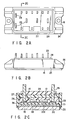
- FIG. 2A is a plan view showing another example of a conventional semiconductor device
- FIG. 2B is a side view thereof
- FIG. 2C is a cross-sectional view taken along the line 2C - 2C of FIG. 2A.
- reference numeral 21 indicates a ceramic substrate.
- a circuit pattern 22 of copper is formed on the mounting surface of the ceramic substrate 21, and a copper layer 30 is formed on the opposite surface of the mounting surface.
- This substrate is a so-called DBC (Direct Bonding Copper) substrate.
- the circuit pattern 22 has a large bed 22a, and semiconductor elements 12 are mounted on the bed 22a.
- a heat dissipation plate 16 is fixed onto the copper layer 30 by solder 23.
- a resin case 24 is adhered to the periphery of the heat dissipation plate 16 through an adhesive layer 25.
- the resin case 24 is filled with a gel material 26 such as silicone resin, and the semiconductor elements 12 and DBC substrate are coated with the gel material 26.
- a casting layer 27 of thermosetting resin is formed on the surface of the gel material 26.
- a terminal holder 28 is provided on the casting layer 27, and pin-like electrode terminals 29 are attached to the terminal holder 28.
- One end of each electrode terminal 29 is electrically connected to the circuit pattern 22 through the casting layer 27 and gel material 26. The other end thereof protrudes from the terminal holder 28 and serves as an outer lead.
- the conventional semiconductor device shown in FIGS. 1A and 1B has a relatively high thermal resistance. This is because thermal conductivity K of the insulative material used for the mold body is considerably smaller than that of ceramics or the like.
- thickness A of the insulative material between the leads 11 and heat radiating plate 16 cannot be decreased to such an extent as to show the same thermal conductivity as that of ceramics.
- thickness A is limited to 0.5 mm, and cannot be set to 0.12 mm or less. Since, furthermore, the average grain diameter of molding resin is about 0.3 mm, if thickness A is set to be smaller than 0.5 mm, a void occurs inevitably, and the semiconductor device is reduced in quality and reliability. Consequently, the conventional semiconductor device shown in FIGS. 1A and 1B is inferior in heat dissipation.
- the conventional semiconductor device of FIGS. 2A to 2C is superior in heat dissipation to that of FIGS. 1A and 1B, it requires a larger number of structural elements and a larger number of manufacturing steps, with the result that the device is complicated and expensive.
- the number of main structural elements of the device shown in FIGS. 1A and 1B is five (lead frame, semiconductor element, heat dissipation plate, bonding wire, and molding resin), while that of the device shown in FIGS. 2A to 2C is nine (DBC substrate, semiconductor element, heat dissipation plate, bonding wire, adhesive for adhering the case, resin case, gel material, casting material, terminal holder including terminal electrode).
- 1A and 1B includes three steps of die bonding, wire bonding, and transfer molding
- the method for manufacturing the device shown in FIGS. 2A to 2C includes six steps of die bonding, wire bonding, mounting of heat dissipation plate and terminal holder (reflow), mounting of resin case (joining), first filling of resin (potting), and second filling of resin (casting).
- An object of the present invention is to provide a semiconductor device which is light, simple and excellent in heat dissipation, and a method for manufacturing the same with high efficiency.
- a semiconductor device comprising a substrate made of an electrically insulative material having a relatively high thermal conductivity, a metallic pattern member provided on one major surface of the substrate and having an external terminal portion extending from the substrate, a semiconductor element mounted on the metallic pattern member, a metallic layer provided on the other major surface of the substrate, a heat dissipation plate fixed onto the metallic layer, and a mold body for coating both the substrate mounted with the semiconductor element and the heat dissipation plate so as to expose the external terminal portion.
- a method for manufacturing a semiconductor device comprising the steps of mounting a semiconductor element on a metallic pattern member provided on one major surface of a substrate made of an electrically insulative material having a relatively high thermal conductivity, the substrate having a metallic layer on the other major surface thereof, fixing a heat dissipation plate onto the metallic layer, and coating both the substrate mounted with the semiconductor element and the heat dissipation plate with an insulative material so as to expose the external terminal portion.
- a semiconductor device of the present invention is featured by comprising a substrate made of an electrically insulative material having a relatively high thermal conductivity, a metallic pattern member provided on one major surface of the substrate and having an external terminal portion extending from the substrate, a semiconductor element mounted on the metallic pattern member, a metallic layer provided on the other major surface of the substrate, a heat dissipation plate fixed onto the metallic layer, and a mold body for coating both the substrate mounted with the semiconductor element and the heat dissipation plate so as to expose the external terminal portion.
- the electrically insulative material for the substrate ceramics such as alumina (Al2O3), aluminum nitride (AlN X ) may be used.
- the material for the metallic pattern member copper, copper alloy and the like may be used.
- the material for the metallic layer copper, copper alloy, and the like may be used.
- a DBC substrate can be used for the substrate having the metallic pattern member and metallic layer.
- the material for the heat dissipation plate aluminum, copper, iron, and the like may be used.
- the material for the mold body epoxy resin, silicone resin, etc may be used.
- the heat generated from the semiconductor element is transmitted to the substrate through the metallic pattern, then transmitted to the heat dissipation plate through the metallic layer, and emitted outside therefrom.
- the heat dissipation of the semiconductor element is therefore improved. Since, furthermore, the external terminal portion of the metallic pattern member can be employed as an external terminal of the semiconductor element, the number of elements constituting the semiconductor device can be decreased, and the semiconductor device can be lightened accordingly.
- a method for manufacturing a semiconductor device is featured by comprising a step of mounting a semiconductor element on a metallic pattern member provided one major surface of a substrate made of an electrically insulative material having a relatively high thermal conductivity, the substrate having a metallic layer on another major surface thereof, a step of fixing a heat dissipation plate onto the metallic layer, and a step of coating both the substrate mounted with the semiconductor element and the heat dissipation plate with an insulative material so as to expose the external terminal portion.
- the step of mounting the semiconductor element on the metallic pattern member of the substrate can be executed by normal die bonding and wire bonding.
- the step of fixing the heat dissipation plate onto the metallic layer can be executed by reflow using a brazing filler such as solder.
- the step of coating both the substrate and heat dissipation plate with the insulative material can be executed by transfer molding using thermosetting resin such as epoxy resin, silicone resin, and the like.
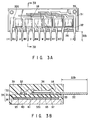
- FIG. 3A is a plan view of a semiconductor device according to the embodiment of the present invention, showing the inside of the device from top
- FIG. 3B is a cross-sectional view taken along the line 3B - 3B of FIG. 3A.
- reference numeral 31 indicates an electrically insulative ceramic substrate having a relatively high thermal conductivity.
- a copper circuit pattern member 32 is provided on the mounting surface of the ceramic substrate 31.
- the pattern member 32 includes a bed 32a having a large area and external terminal portions 32b extending from the ceramic substrate 31.
- An alloy layer 33 of ceramic and copper is formed between the ceramic substrate 31 and copper circuit pattern member 32 to fix the pattern member 32 onto the substrate 31.
- a copper layer 34 is fixed onto the opposite surface (hereinafter referred to as the undersurface) of the mounting surface of the ceramic substrate 31 by means of the alloy layer 33.
- the ceramic substrate 31, copper circuit pattern member 32, and copper layer 34 constitute a DBC (Direct Bonding Copper) substrate 35.
- Power device pellets 36 each incorporating a power transistor, a power IC or the like, are mounted on the bed 32a. More specifically, the pellets 36 are fixed onto the bed 32a by solder 37 and electrically connected to the copper circuit pattern member 32. It is preferable that high melting point solder such as Pb-Sn-Ag series solder should be used as the solder 37. In this embodiment, high melting point solder having a melting point of about 310°C is employed. Electrode pads (not shown) are provided on the surfaces of the pellets 36 and electrically connected to the copper circuit pattern member 32 by bonding wires 38 of gold (Au), aluminum (Al) or the like.
- Au gold
- Al aluminum
- a heat dissipation plate 40 is mounted on the copper layer 34 by means of solder 41 such as Pb-Sn series solder.
- the plate 40 is exposed to outside and serves to cause the heat generated from the pellets 36 to dissipate outside the device.
- a substantially cuboid-shaped mold body 39 is provided around the DBC substrate 35 to coat both the DBC substrate 35 mounted with the pellets 36 and the heat dissipation plate 40 such that the external terminal portion 32b of the copper circuit pattern member 32 is exposed.
- the mold body 39 electrically insulates the pellets 36 from outside.
- the exposed external terminal portion 32b is used as an outer lead.
- the semiconductor device of the present invention having the above constitution is directed to a motor driving inverter circuit device.
- the inverter circuit device incorporates six pellets 36 and its circuit diagram is shown in FIG. 4. Referring to FIG. 4, each of the pellets 36 has a base terminal, a collector terminal, and an emitter terminal, and functions as a single power device (a bipolar transistor in this embodiment).
- the pellet 36 includes Darlington-connected two power transistors (of a bipolar type), a diode, a resistor, and the like, and is formed as an integrated circuit or a sort of power IC which is capable of driving a large current.
- the motor driving inverter circuit shown in FIG. 4 is constituted by the six pellets 36 including the power devices or power ICs. All the pellets 36 are incorporated in a single envelope to serve as one resin-molded semiconductor device. It is therefore eleven outer leads that protrude from the mold body 39 and include a positive power supply terminal (+), a negative power supply terminal (-), six input terminals BU, BV, BW, BX, BY and BZ, and three output terminals U, V and W.
- FIG. 3A the same reference numerals as those of FIG. 4 are shown in the vicinity of the outer leads.
- FIG. 5A is a plan view of the DBC substrate 35 of the semiconductor device according to the embodiment of the present invention
- FIG. 5B is a cross-sectional view taken along the line 5B - 5B of FIG. 5A.
- the DBC substrate 35 has a tie bar 42 for connecting the external terminal portions 32b, in the vicinity of the end portion of the copper circuit pattern member 32, thereby to form a lead frame. Since the pattern member 32 is in the shape of a lead frame, the semiconductor device can be assembled continuously.
- the manufacturing method will be described more specifically.
- a DBC substrate 35 provided with a copper circuit pattern member 32 in the shape of a lead frame is prepared, as shown in FIGS. 5A and 5B.
- Pellets 36 are fixed onto a bed 32a formed on the pattern member 32 using high melting point solder 37 (die bonding), and electrode pads (not shown) provided on the pellets 36 and copper circuit pattern member 32 are electrically connected to each other by use of bonding wires 38 of gold (Au), aluminum (Al) or the like (wire bonding).
- a metallic heat dissipation plate 40 is fixed onto the undersurface of the DBC substrate 35, i.e., onto the surface of copper layer 34, using solder 41 (mounting of heat dissipation plate by reflow).
- the DBC substrate 35 mounted with the heat dissipation plate 40 is located in a mold (not shown), and resin is caused to pour into the mold for transfer molding, thereby forming a cuboid-like mold body 39 around the DBC substrate 35 (molding). Finally a tie bar 42 connecting the external terminal portions 32b of the copper circuit pattern member 32 is cut and removed, and the portions 32b are formed into a desired shape (outer lead forming). By doing so, the semiconductor device of the present invention is obtained.
- the pellets 36 are virtually placed into contact with the ceramic substrate 31 simply through the copper circuit pattern member 32. For this reason, the heat generated from the pellets 36 is transmitted to the ceramic substrate 31 formed of a material having a relatively high thermal conductivity, through the copper circuit pattern member 32, then transmitted to the heat dissipation plate 40 through the copper layer 34, and emitted outside therefrom. Therefore, the heat dissipation of the pellets 36 can be improved more than that of the conventional semiconductor device (shown in FIGS. 1A and 1B) which is so constructed that resin is inserted under the bed on which the pellets are placed.
- the thermal resistance of the envelope of the conventional semiconductor device is about 4°C/W for each power device pellet of 5 mm2, while that of the envelope of the semiconductor device of the present invention is reduced to less than half of 4°C/W, that is, about 1.5°C/W for each power device pellet of 5 mm2.
- the DBC substrate can stably be coated when the mold body is formed by the transfer molding. Since the copper circuit pattern member is reliably supported, its thickness can be decreased.
- the external terminal sections 32b of the copper circuit pattern member 32 are extended from the ceramic substrate 31 and used as external electrode terminals of the pellets 36.
- the copper circuit pattern member 32 as external electrode terminals, the number of structural elements of the semiconductor device can be reduced, and the cost for the elements can be lowered accordingly. Since the structural elements of the semiconductor device can be decreased in number, the number of steps of manufacturing the device can be reduced, thereby lowering the manufacture cost.
- the conventional semiconductor device shown in FIGS. 2A to 2C is likely to be expensive since it requires a large number of structural elements.
- the number of main structural elements has only to be five, that is, the DBC substrate, pellets, heat dissipation plate, wires, and resin, and the number can be decreased by four, compared with that of structural elements for the conventional device shown in FIGS. 2A to 2C.
- the number of manufacture steps has only to be five, that is, die bonding, wire bonding, mounting of heat dissipation plate using reflow, molding, and outer lead forming, which is less than that of manufacturing steps of the conventional device by one. As a result, the manufacture cost can be lowered further.
- the copper circuit pattern member is formed in the shape of a lead frame, resin molding operations such as transfer molding can be performed continuously and simultaneously.
- resin molding operations such as transfer molding can be performed continuously and simultaneously.
- a resin molding operation has to be performed for each individual product, which is inferior in mass productivity and operability, whereas the manufacture method of the present invention is very effective in mass productivity and operability.
- the present invention is not limited to the above embodiment.
- aluminum nitride AlN X
- AlN X aluminum nitride
- the aluminum nitride is more expensive than the alumina, and a direct bonding method such as a DBC method cannot be applied to the aluminum nitride, its thermal conductivity is higher than that of the alumina and suitable to improve in heat dissipation.
- the substrate 31 can be fixed onto the copper circuit pattern member 32 by using a brazing filler containing an element of group IV of the periodic table, such as Ti.
- the bonding method using the brazing filler is generally called active metal bonding.
- the semiconductor device according to the present invention is light, simple, and excellent in heat dissipation, and can be obtained with efficiency.
Landscapes
- Cooling Or The Like Of Semiconductors Or Solid State Devices (AREA)
- Lead Frames For Integrated Circuits (AREA)
- Structures Or Materials For Encapsulating Or Coating Semiconductor Devices Or Solid State Devices (AREA)
Abstract
Description
- The present invention relates to a semiconductor device mounting a power transistor, a power IC, or the like and a method for manufacturing the same.
- A conventional resin-molded semiconductor device mounting power devices such as a power transistor and a power IC, is so constructed that the power devices are electrically insulated from an envelope (a peripheral member of the semiconductor device) other than the external electrode terminals (leads) in order to prevent an electrical short circuit from occurring between the power devices or between the power devices and externally-mounted heat dissipation plate. This type of conventional semiconductor device is shown in FIGS. 1A, 1B and 2A to 2C.
- FIG. 1A is a plan view showing the inside of a conventional semiconductor device, and FIG. 1B is a cross-sectional view taken along the
line 1B - 1B of FIG. 1A. In these Figures,reference numeral 11 indicates leads. Theleads 11 include alarge bed 11a, andsemiconductor elements 12 are mounted on thebed 11a. Thesemiconductor elements 12 are fixed onto thebed 11a bysolder 13 and electrically connected to theleads 11. Theleads 11 constitute a lead frame. Electrode pads (not shown) are provided on the upper surfaces of thesemiconductor elements 12 and electrically connected to theleads 11 bybonding wires 14. - The
leads 11 mounted with thesemiconductor elements 12 are coated with an insulative material such as epoxy resin in order to electrically insulate thesemiconductor elements 12 from outside. Part of each of theleads 11 protrudes from amold body 15 formed of an insulative material, and this protruding part serves as an outer lead. Aheat dissipation plate 16 formed of metal such as Al or Cu, is provided through an insulating layer under those surfaces of theleads 11 which are opposite to the surfaces thereof mounted with thesemiconductor elements 12, and theinsulative mold body 15 is formed between theleads 11 andplate 16. Themold body 15 can be obtained by arranging theleads 11 mounted with thesemiconductor elements 12 andheat dissipation plate 16 at regular intervals and then by transfer molding using the insulative material. - FIG. 2A is a plan view showing another example of a conventional semiconductor device, FIG. 2B is a side view thereof, and FIG. 2C is a cross-sectional view taken along the
line 2C - 2C of FIG. 2A. In FIGS. 2A to 2C, the same components as those in FIGS. 1A and 1B are denoted by the same reference numerals and their descriptions are omitted. In FIG. 2C,reference numeral 21 indicates a ceramic substrate. Acircuit pattern 22 of copper is formed on the mounting surface of theceramic substrate 21, and acopper layer 30 is formed on the opposite surface of the mounting surface. This substrate is a so-called DBC (Direct Bonding Copper) substrate. Thecircuit pattern 22 has a large bed 22a, andsemiconductor elements 12 are mounted on the bed 22a. - A
heat dissipation plate 16 is fixed onto thecopper layer 30 bysolder 23. Aresin case 24 is adhered to the periphery of theheat dissipation plate 16 through anadhesive layer 25. Theresin case 24 is filled with agel material 26 such as silicone resin, and thesemiconductor elements 12 and DBC substrate are coated with thegel material 26. Acasting layer 27 of thermosetting resin is formed on the surface of thegel material 26. Further, aterminal holder 28 is provided on thecasting layer 27, and pin-like electrode terminals 29 are attached to theterminal holder 28. One end of eachelectrode terminal 29 is electrically connected to thecircuit pattern 22 through thecasting layer 27 andgel material 26. The other end thereof protrudes from theterminal holder 28 and serves as an outer lead. - In the foregoing resin-sealed semiconductor devices incorporating power devices, it is important to cause the heat generated from the power devices to quickly dissipate outside, that is, to improve the property of dissipation heat. Therefore, the characteristics of the power devices can be made effective, and the reliability of the device can be maintained even after the device is used for a long time. It is thus very important to reduce thermal resistance applied from the power devices to the surface of the envelope (peripheral member) in order to improve the property of heat dissipation from the power devices.
- However, the conventional semiconductor device shown in FIGS. 1A and 1B has a relatively high thermal resistance. This is because thermal conductivity K of the insulative material used for the mold body is considerably smaller than that of ceramics or the like.
- Because of restrictions on the manufacture technology, thickness A of the insulative material between the
leads 11 and heatradiating plate 16 cannot be decreased to such an extent as to show the same thermal conductivity as that of ceramics. For example, if the semiconductor device shown in FIG. 1B is manufactured by use of molding resin having the highest thermal conductivity on the market (
- According to the current manufacture technique, however, thickness A is limited to 0.5 mm, and cannot be set to 0.12 mm or less. Since, furthermore, the average grain diameter of molding resin is about 0.3 mm, if thickness A is set to be smaller than 0.5 mm, a void occurs inevitably, and the semiconductor device is reduced in quality and reliability. Consequently, the conventional semiconductor device shown in FIGS. 1A and 1B is inferior in heat dissipation.
- Though the conventional semiconductor device of FIGS. 2A to 2C is superior in heat dissipation to that of FIGS. 1A and 1B, it requires a larger number of structural elements and a larger number of manufacturing steps, with the result that the device is complicated and expensive. For example, the number of main structural elements of the device shown in FIGS. 1A and 1B is five (lead frame, semiconductor element, heat dissipation plate, bonding wire, and molding resin), while that of the device shown in FIGS. 2A to 2C is nine (DBC substrate, semiconductor element, heat dissipation plate, bonding wire, adhesive for adhering the case, resin case, gel material, casting material, terminal holder including terminal electrode). The method for manufacturing the device shown in FIGS. 1A and 1B includes three steps of die bonding, wire bonding, and transfer molding, whereas the method for manufacturing the device shown in FIGS. 2A to 2C includes six steps of die bonding, wire bonding, mounting of heat dissipation plate and terminal holder (reflow), mounting of resin case (joining), first filling of resin (potting), and second filling of resin (casting).
- An object of the present invention is to provide a semiconductor device which is light, simple and excellent in heat dissipation, and a method for manufacturing the same with high efficiency.
- To attain the above object, there is provided a semiconductor device comprising a substrate made of an electrically insulative material having a relatively high thermal conductivity, a metallic pattern member provided on one major surface of the substrate and having an external terminal portion extending from the substrate, a semiconductor element mounted on the metallic pattern member, a metallic layer provided on the other major surface of the substrate, a heat dissipation plate fixed onto the metallic layer, and a mold body for coating both the substrate mounted with the semiconductor element and the heat dissipation plate so as to expose the external terminal portion.
- To attain the above object, there is also provided a method for manufacturing a semiconductor device, comprising the steps of mounting a semiconductor element on a metallic pattern member provided on one major surface of a substrate made of an electrically insulative material having a relatively high thermal conductivity, the substrate having a metallic layer on the other major surface thereof, fixing a heat dissipation plate onto the metallic layer, and coating both the substrate mounted with the semiconductor element and the heat dissipation plate with an insulative material so as to expose the external terminal portion.
- This invention can be more fully understood from the following detailed description when taken in conjunction with the accompanying drawings, in which:
- FIG. 1A is a plan view showing a conventional semiconductor device;
- FIG. 1B is a cross-sectional view taken along the
line 1B - 1B of FIG. 1A; - FIG. 2A is a plan view showing another conventional semiconductor device;
- FIG. 2B is a side view of the semiconductor device shown in FIG. 2A;
- FIG. 2C is a cross-sectional view taken along the
line 2C - 2C of FIG. 2A; - FIG. 3A is a plan view showing a semiconductor device according to one embodiment of the present invention;
- FIG. 3B is a cross-sectional view taken along the
line 3B - 3B of FIG. 3A; - FIG. 4 is a circuit diagram for explaining a circuit of the semiconductor device shown in FIG. 3A;
- FIG. 5A is a plan view showing a DBC substrate of the semiconductor device of the present invention; and
- FIG. 5B is a cross-sectional view taken along the
line 5B - 5B of FIG. 5A. - A semiconductor device of the present invention is featured by comprising a substrate made of an electrically insulative material having a relatively high thermal conductivity, a metallic pattern member provided on one major surface of the substrate and having an external terminal portion extending from the substrate, a semiconductor element mounted on the metallic pattern member, a metallic layer provided on the other major surface of the substrate, a heat dissipation plate fixed onto the metallic layer, and a mold body for coating both the substrate mounted with the semiconductor element and the heat dissipation plate so as to expose the external terminal portion.
- As the electrically insulative material for the substrate, ceramics such as alumina (Al₂O₃), aluminum nitride (AlNX) may be used. As the material for the metallic pattern member, copper, copper alloy and the like may be used. Further, as the material for the metallic layer, copper, copper alloy, and the like may be used. A DBC substrate can be used for the substrate having the metallic pattern member and metallic layer. As the material for the heat dissipation plate, aluminum, copper, iron, and the like may be used. As the material for the mold body, epoxy resin, silicone resin, etc may be used.
- In the semiconductor device having the above constitution, the heat generated from the semiconductor element is transmitted to the substrate through the metallic pattern, then transmitted to the heat dissipation plate through the metallic layer, and emitted outside therefrom. The heat dissipation of the semiconductor element is therefore improved. Since, furthermore, the external terminal portion of the metallic pattern member can be employed as an external terminal of the semiconductor element, the number of elements constituting the semiconductor device can be decreased, and the semiconductor device can be lightened accordingly.
- A method for manufacturing a semiconductor device according to the present invention is featured by comprising a step of mounting a semiconductor element on a metallic pattern member provided one major surface of a substrate made of an electrically insulative material having a relatively high thermal conductivity, the substrate having a metallic layer on another major surface thereof, a step of fixing a heat dissipation plate onto the metallic layer, and a step of coating both the substrate mounted with the semiconductor element and the heat dissipation plate with an insulative material so as to expose the external terminal portion.
- The step of mounting the semiconductor element on the metallic pattern member of the substrate can be executed by normal die bonding and wire bonding. The step of fixing the heat dissipation plate onto the metallic layer can be executed by reflow using a brazing filler such as solder. The step of coating both the substrate and heat dissipation plate with the insulative material can be executed by transfer molding using thermosetting resin such as epoxy resin, silicone resin, and the like.
- The steps of the above-described method according to the present invention can be simplified since the structural elements of the semiconductor device are decreased in number. Consequently, the semiconductor device which is excellent in heat dissipation can be manufactured with efficiency and at low cost.
- An embodiment of the present invention will now be described, with reference to the accompanying drawings.
- FIG. 3A is a plan view of a semiconductor device according to the embodiment of the present invention, showing the inside of the device from top, and FIG. 3B is a cross-sectional view taken along the
line 3B - 3B of FIG. 3A. In these figures,reference numeral 31 indicates an electrically insulative ceramic substrate having a relatively high thermal conductivity. A coppercircuit pattern member 32 is provided on the mounting surface of theceramic substrate 31. Thepattern member 32 includes a bed 32a having a large area and externalterminal portions 32b extending from theceramic substrate 31. Analloy layer 33 of ceramic and copper is formed between theceramic substrate 31 and coppercircuit pattern member 32 to fix thepattern member 32 onto thesubstrate 31. Further, acopper layer 34 is fixed onto the opposite surface (hereinafter referred to as the undersurface) of the mounting surface of theceramic substrate 31 by means of thealloy layer 33. Theceramic substrate 31, coppercircuit pattern member 32, andcopper layer 34 constitute a DBC (Direct Bonding Copper)substrate 35. -
Power device pellets 36 each incorporating a power transistor, a power IC or the like, are mounted on the bed 32a. More specifically, thepellets 36 are fixed onto the bed 32a bysolder 37 and electrically connected to the coppercircuit pattern member 32. It is preferable that high melting point solder such as Pb-Sn-Ag series solder should be used as thesolder 37. In this embodiment, high melting point solder having a melting point of about 310°C is employed. Electrode pads (not shown) are provided on the surfaces of thepellets 36 and electrically connected to the coppercircuit pattern member 32 bybonding wires 38 of gold (Au), aluminum (Al) or the like. - A
heat dissipation plate 40 is mounted on thecopper layer 34 by means ofsolder 41 such as Pb-Sn series solder. Theplate 40 is exposed to outside and serves to cause the heat generated from thepellets 36 to dissipate outside the device. - A substantially cuboid-shaped
mold body 39 is provided around theDBC substrate 35 to coat both theDBC substrate 35 mounted with thepellets 36 and theheat dissipation plate 40 such that theexternal terminal portion 32b of the coppercircuit pattern member 32 is exposed. Themold body 39 electrically insulates thepellets 36 from outside. The exposed externalterminal portion 32b is used as an outer lead. - The semiconductor device of the present invention having the above constitution is directed to a motor driving inverter circuit device. The inverter circuit device incorporates six
pellets 36 and its circuit diagram is shown in FIG. 4. Referring to FIG. 4, each of thepellets 36 has a base terminal, a collector terminal, and an emitter terminal, and functions as a single power device (a bipolar transistor in this embodiment). Thepellet 36 includes Darlington-connected two power transistors (of a bipolar type), a diode, a resistor, and the like, and is formed as an integrated circuit or a sort of power IC which is capable of driving a large current. - The motor driving inverter circuit shown in FIG. 4 is constituted by the six
pellets 36 including the power devices or power ICs. All thepellets 36 are incorporated in a single envelope to serve as one resin-molded semiconductor device. It is therefore eleven outer leads that protrude from themold body 39 and include a positive power supply terminal (+), a negative power supply terminal (-), six input terminals BU, BV, BW, BX, BY and BZ, and three output terminals U, V and W. In FIG. 3A, the same reference numerals as those of FIG. 4 are shown in the vicinity of the outer leads. - A method for manufacturing the semiconductor device shown in FIG. 3 will now be described. FIG. 5A is a plan view of the
DBC substrate 35 of the semiconductor device according to the embodiment of the present invention, and FIG. 5B is a cross-sectional view taken along theline 5B - 5B of FIG. 5A. As illustrated in FIG. 5A, theDBC substrate 35 has atie bar 42 for connecting the externalterminal portions 32b, in the vicinity of the end portion of the coppercircuit pattern member 32, thereby to form a lead frame. Since thepattern member 32 is in the shape of a lead frame, the semiconductor device can be assembled continuously. - The manufacturing method will be described more specifically.
- First a
DBC substrate 35 provided with a coppercircuit pattern member 32 in the shape of a lead frame, is prepared, as shown in FIGS. 5A and 5B.Pellets 36 are fixed onto a bed 32a formed on thepattern member 32 using high melting point solder 37 (die bonding), and electrode pads (not shown) provided on thepellets 36 and coppercircuit pattern member 32 are electrically connected to each other by use ofbonding wires 38 of gold (Au), aluminum (Al) or the like (wire bonding). Then a metallicheat dissipation plate 40 is fixed onto the undersurface of theDBC substrate 35, i.e., onto the surface ofcopper layer 34, using solder 41 (mounting of heat dissipation plate by reflow). After that, theDBC substrate 35 mounted with theheat dissipation plate 40 is located in a mold (not shown), and resin is caused to pour into the mold for transfer molding, thereby forming a cuboid-like mold body 39 around the DBC substrate 35 (molding). Finally atie bar 42 connecting the externalterminal portions 32b of the coppercircuit pattern member 32 is cut and removed, and theportions 32b are formed into a desired shape (outer lead forming). By doing so, the semiconductor device of the present invention is obtained. - According to the semiconductor device described above, since the copper
circuit pattern member 32 almost directly contacts theceramic substrate 31, thepellets 36 are virtually placed into contact with theceramic substrate 31 simply through the coppercircuit pattern member 32. For this reason, the heat generated from thepellets 36 is transmitted to theceramic substrate 31 formed of a material having a relatively high thermal conductivity, through the coppercircuit pattern member 32, then transmitted to theheat dissipation plate 40 through thecopper layer 34, and emitted outside therefrom. Therefore, the heat dissipation of thepellets 36 can be improved more than that of the conventional semiconductor device (shown in FIGS. 1A and 1B) which is so constructed that resin is inserted under the bed on which the pellets are placed. More specifically, the thermal resistance of the envelope of the conventional semiconductor device is about 4°C/W for each power device pellet of 5 mm², while that of the envelope of the semiconductor device of the present invention is reduced to less than half of 4°C/W, that is, about 1.5°C/W for each power device pellet of 5 mm². - According to the semiconductor device having the above constitution, since the copper circuit pattern member is supported by the ceramic substrate, the DBC substrate can stably be coated when the mold body is formed by the transfer molding. Since the copper circuit pattern member is reliably supported, its thickness can be decreased.
- In the semiconductor device of the present invention, the external
terminal sections 32b of the coppercircuit pattern member 32 are extended from theceramic substrate 31 and used as external electrode terminals of thepellets 36. Using the coppercircuit pattern member 32 as external electrode terminals, the number of structural elements of the semiconductor device can be reduced, and the cost for the elements can be lowered accordingly. Since the structural elements of the semiconductor device can be decreased in number, the number of steps of manufacturing the device can be reduced, thereby lowering the manufacture cost. For example, the conventional semiconductor device shown in FIGS. 2A to 2C is likely to be expensive since it requires a large number of structural elements. However, in the semiconductor device of the present invention, the number of main structural elements has only to be five, that is, the DBC substrate, pellets, heat dissipation plate, wires, and resin, and the number can be decreased by four, compared with that of structural elements for the conventional device shown in FIGS. 2A to 2C. Moreover, in the embodiment of the present invention, the number of manufacture steps has only to be five, that is, die bonding, wire bonding, mounting of heat dissipation plate using reflow, molding, and outer lead forming, which is less than that of manufacturing steps of the conventional device by one. As a result, the manufacture cost can be lowered further. - In the foregoing semiconductor device of the present invention, since the copper circuit pattern member is formed in the shape of a lead frame, resin molding operations such as transfer molding can be performed continuously and simultaneously. In the conventional semiconductor device shown in FIG. 2, a resin molding operation has to be performed for each individual product, which is inferior in mass productivity and operability, whereas the manufacture method of the present invention is very effective in mass productivity and operability.
- The present invention is not limited to the above embodiment. For example, in place of the aluminum, aluminum nitride (AlNX) can be used as a material for the
ceramic substrate 31. Though the aluminum nitride is more expensive than the alumina, and a direct bonding method such as a DBC method cannot be applied to the aluminum nitride, its thermal conductivity is higher than that of the alumina and suitable to improve in heat dissipation. When the aluminum nitride is used for theceramic substrate 31, thesubstrate 31 can be fixed onto the coppercircuit pattern member 32 by using a brazing filler containing an element of group IV of the periodic table, such as Ti. The bonding method using the brazing filler is generally called active metal bonding. - As described above, the semiconductor device according to the present invention is light, simple, and excellent in heat dissipation, and can be obtained with efficiency.
Claims (17)
- A semiconductor device comprising:
a substrate (31) made of an electrically insulative material having a relatively high thermal conductivity;
a metallic pattern member (32) provided on one major surface of said substrate and having an external terminal portion extending from said substrate;
a semiconductor element (36) mounted on said metallic pattern member;
a metallic layer (34) provided on another major surface of said substrate;
a heat dissipation plate (40) fixed onto said metallic layer; and
a mold body (39) for coating both said substrate mounted with said semiconductor element and said heat dissipation plate so as to expose the external terminal portion (32b). - The semiconductor device according to claim 1, characterized in that said substrate is made of alumina of aluminum nitride.
- The semiconductor device according to claim 1, characterized in that said metallic pattern member is made of copper or copper alloy.
- The semiconductor device according to claim 1, characterized in that said metallic layer is made of copper or copper alloy.
- The semiconductor device according to claim 1, characterized in that said heat dissipation plate is made of one selected from the group consisting of aluminum, copper, and iron.
- The semiconductor device according to claim 1, characterized in that said mold body is made of epoxy resin or silicone resin.
- The semiconductor device according to claim 1, characterized in that said metallic pattern member and said substrate are bonded to each other by using a brazing filler.
- The semiconductor device according to claim 7, characterized in that said brazing filler is made of high melting point solder or brazing filler containing an element of group IV of the periodic table.
- The semiconductor device according to claim 1, characterized in that said heat dissipation plate and said metallic layer are bonded to each other by using a brazing filler.
- The semiconductor device according to claim 9, characterized in that said brazing filler is made of solder or metal paste.
- The semiconductor device according to claim 1, characterized in that said semiconductor element is at least one selected from the group consisting of a power transistor and a power IC.
- A method for manufacturing a semiconductor device, comprising the steps of:
mounting a semiconductor element (36) on a metallic pattern member (32) provided on one major surface of a substrate (31) made of an electrically insulative material having a relatively high thermal conductivity, said substrate having a metallic layer (34) on another major surface thereof;
fixing a heat dissipation plate (40) onto said metallic layer; and
coating both said substrate mounted with said semiconductor element and said heat dissipation plate with an insulative material so as to expose the external terminal portion. - The method according to claim 12, characterized in that said metallic pattern member has a distal end connected to the external terminal portion (32b).
- The method according to claim 12, characterized in that said semiconductor element is mounted on said metallic pattern member by die bonding and wire bonding.
- The method according to claim 12, characterized in that said heat dissipation plate is fixed onto said metallic layer by heat treatment using a brazing filler.
- The method according to claim 12, characterized in that said substrate mounted with said semiconductor element, and said heat dissipation plate are coated with an insulative material by transfer molding.
- The method according to claim 16, characterized in that said insulative material is epoxy resin or silicone resin.
Applications Claiming Priority (2)
| Application Number | Priority Date | Filing Date | Title |
|---|---|---|---|
| JP266336/93 | 1993-10-25 | ||
| JP26633693 | 1993-10-25 |
Publications (2)
| Publication Number | Publication Date |
|---|---|
| EP0650193A2 true EP0650193A2 (en) | 1995-04-26 |
| EP0650193A3 EP0650193A3 (en) | 1996-07-31 |
Family
ID=17429525
Family Applications (1)
| Application Number | Title | Priority Date | Filing Date |
|---|---|---|---|
| EP94115966A Ceased EP0650193A3 (en) | 1993-10-25 | 1994-10-10 | Semiconductor device and method for its manufacture. |
Country Status (3)
| Country | Link |
|---|---|
| US (1) | US5783466A (en) |
| EP (1) | EP0650193A3 (en) |
| KR (1) | KR100191759B1 (en) |
Cited By (1)
| Publication number | Priority date | Publication date | Assignee | Title |
|---|---|---|---|---|
| US6914321B2 (en) | 2001-02-20 | 2005-07-05 | Mitsubishi Denki Kabushiki Kaisha | Semiconductor device |
Families Citing this family (15)
| Publication number | Priority date | Publication date | Assignee | Title |
|---|---|---|---|---|
| JPH0964240A (en) * | 1995-08-25 | 1997-03-07 | Toshiba Corp | Semiconductor device and method of manufacturing semiconductor device |
| US6404065B1 (en) | 1998-07-31 | 2002-06-11 | I-Xys Corporation | Electrically isolated power semiconductor package |
| US6335548B1 (en) * | 1999-03-15 | 2002-01-01 | Gentex Corporation | Semiconductor radiation emitter package |
| US6864574B1 (en) * | 1999-11-29 | 2005-03-08 | Matsushita Electric Industrial Co., Ltd. | Semiconductor package |
| US6583505B2 (en) * | 2001-05-04 | 2003-06-24 | Ixys Corporation | Electrically isolated power device package |
| US6727585B2 (en) * | 2001-05-04 | 2004-04-27 | Ixys Corporation | Power device with a plastic molded package and direct bonded substrate |
| US6731002B2 (en) | 2001-05-04 | 2004-05-04 | Ixys Corporation | High frequency power device with a plastic molded package and direct bonded substrate |
| US6818477B2 (en) * | 2001-11-26 | 2004-11-16 | Powerwave Technologies, Inc. | Method of mounting a component in an edge-plated hole formed in a printed circuit board |
| KR100902766B1 (en) * | 2002-09-27 | 2009-06-15 | 페어차일드코리아반도체 주식회사 | Discrete Packages with Insulated Ceramic Heat Sink |
| JP2005005642A (en) * | 2003-06-16 | 2005-01-06 | Nec Tokin Corp | Chip-type solid electrolytic capacitor and manufacturing method thereof |
| JP2006253183A (en) * | 2005-03-08 | 2006-09-21 | Hitachi Ltd | Semiconductor power module |
| US8269338B2 (en) * | 2006-08-10 | 2012-09-18 | Vishay General Semiconductor Llc | Semiconductor device having improved heat dissipation capabilities |
| CN102548341A (en) * | 2010-12-10 | 2012-07-04 | 旭丽电子(广州)有限公司 | Heat dissipation shell structure |
| US9245880B2 (en) * | 2013-10-28 | 2016-01-26 | Mosway Semiconductor Limited | High voltage semiconductor power switching device |
| CN106920781A (en) * | 2015-12-28 | 2017-07-04 | 意法半导体有限公司 | Semiconductor package body and the method for forming semiconductor package body |
Family Cites Families (8)
| Publication number | Priority date | Publication date | Assignee | Title |
|---|---|---|---|---|
| US3829598A (en) * | 1972-09-25 | 1974-08-13 | Hutson Ind Inc | Copper heat sinks for electronic devices and method of making same |
| US4129243A (en) * | 1975-07-30 | 1978-12-12 | General Electric Company | Double side cooled, pressure mounted semiconductor package and process for the manufacture thereof |
| JPS5753947A (en) * | 1980-09-17 | 1982-03-31 | Hitachi Ltd | Transistor and electronic device containing it |
| JPS5968958A (en) * | 1982-10-12 | 1984-04-19 | Mitsubishi Electric Corp | Gate turn-off thyristor assembled body |
| JPS60113931A (en) * | 1983-11-25 | 1985-06-20 | Toshiba Corp | Semiconductor device |
| DE3684184D1 (en) * | 1985-06-20 | 1992-04-16 | Toshiba Kawasaki Kk | ENCLOSED SEMICONDUCTOR ARRANGEMENT. |
| US5317194A (en) * | 1989-10-17 | 1994-05-31 | Kabushiki Kaisha Toshiba | Resin-sealed semiconductor device having intermediate silicon thermal dissipation means and embedded heat sink |
| JPH05267500A (en) * | 1992-03-19 | 1993-10-15 | Toshiba Corp | Resin-sealed semiconductor device |
-
1994
- 1994-10-10 EP EP94115966A patent/EP0650193A3/en not_active Ceased
- 1994-10-25 KR KR1019940027250A patent/KR100191759B1/en not_active Expired - Fee Related
-
1997
- 1997-03-20 US US08/821,385 patent/US5783466A/en not_active Expired - Lifetime
Cited By (2)
| Publication number | Priority date | Publication date | Assignee | Title |
|---|---|---|---|---|
| US6914321B2 (en) | 2001-02-20 | 2005-07-05 | Mitsubishi Denki Kabushiki Kaisha | Semiconductor device |
| DE10149580B4 (en) * | 2001-02-20 | 2009-07-16 | Mitsubishi Denki K.K. | Semiconductor device |
Also Published As
| Publication number | Publication date |
|---|---|
| US5783466A (en) | 1998-07-21 |
| EP0650193A3 (en) | 1996-07-31 |
| KR950012694A (en) | 1995-05-16 |
| KR100191759B1 (en) | 1999-06-15 |
Similar Documents
| Publication | Publication Date | Title |
|---|---|---|
| KR100342589B1 (en) | Semiconductor power modules and methods for manufacturing the same | |
| JP5442368B2 (en) | IC chip package with direct lead wire | |
| US6552417B2 (en) | Molded plastic package with heat sink and enhanced electrical performance | |
| US6724071B2 (en) | Molded plastic package with heat sink and enhanced electrical performance | |
| US6731002B2 (en) | High frequency power device with a plastic molded package and direct bonded substrate | |
| US5521429A (en) | Surface-mount flat package semiconductor device | |
| US7202557B2 (en) | Co-packaged control circuit, transistor and inverted diode | |
| US5198964A (en) | Packaged semiconductor device and electronic device module including same | |
| KR101311635B1 (en) | Surface mount light emitting chip package | |
| US5783466A (en) | Semiconductor device and method of manufacturing the same | |
| JPH0758277A (en) | Semiconductor device | |
| US5616886A (en) | Wirebondless module package | |
| US5910681A (en) | Resin sealed semiconductor device | |
| US20220310409A1 (en) | Method to connect power terminal to substrate within semiconductor package | |
| JP4886104B2 (en) | Power semiconductor packaging package with ball grid array | |
| JPH11191561A (en) | Method for manufacturing semiconductor device | |
| US7102211B2 (en) | Semiconductor device and hybrid integrated circuit device | |
| US6876067B2 (en) | Semiconductor device | |
| JPH07176664A (en) | Semiconductor device and manufacturing method thereof | |
| JPH11163007A (en) | Method for manufacturing semiconductor device | |
| KR100244826B1 (en) | A semiconductor device and method for manufacturing the same | |
| JP2003224234A (en) | Semiconductor device | |
| JPH11220074A (en) | Semiconductor device | |
| JP2736161B2 (en) | Semiconductor device | |
| KR100260996B1 (en) | Array type semiconductor package using a lead frame and its manufacturing method |
Legal Events
| Date | Code | Title | Description |
|---|---|---|---|
| PUAI | Public reference made under article 153(3) epc to a published international application that has entered the european phase |
Free format text: ORIGINAL CODE: 0009012 |
|
| 17P | Request for examination filed |
Effective date: 19941010 |
|
| AK | Designated contracting states |
Kind code of ref document: A2 Designated state(s): DE FR GB |
|
| PUAL | Search report despatched |
Free format text: ORIGINAL CODE: 0009013 |
|
| AK | Designated contracting states |
Kind code of ref document: A3 Designated state(s): DE FR GB |
|
| 17Q | First examination report despatched |
Effective date: 19970919 |
|
| APAB | Appeal dossier modified |
Free format text: ORIGINAL CODE: EPIDOS NOAPE |
|
| APAB | Appeal dossier modified |
Free format text: ORIGINAL CODE: EPIDOS NOAPE |
|
| APAD | Appeal reference recorded |
Free format text: ORIGINAL CODE: EPIDOS REFNE |
|
| APBT | Appeal procedure closed |
Free format text: ORIGINAL CODE: EPIDOSNNOA9E |
|
| STAA | Information on the status of an ep patent application or granted ep patent |
Free format text: STATUS: THE APPLICATION HAS BEEN REFUSED |
|
| 18R | Application refused |
Effective date: 20031118 |
|
| APAF | Appeal reference modified |
Free format text: ORIGINAL CODE: EPIDOSCREFNE |