EP0651309A2 - Régulateur de tension CMOS embarqué - Google Patents
Régulateur de tension CMOS embarqué Download PDFInfo
- Publication number
- EP0651309A2 EP0651309A2 EP94114202A EP94114202A EP0651309A2 EP 0651309 A2 EP0651309 A2 EP 0651309A2 EP 94114202 A EP94114202 A EP 94114202A EP 94114202 A EP94114202 A EP 94114202A EP 0651309 A2 EP0651309 A2 EP 0651309A2
- Authority
- EP
- European Patent Office
- Prior art keywords
- voltage
- reference voltage
- node
- coupled
- semiconductor device
- Prior art date
- Legal status (The legal status is an assumption and is not a legal conclusion. Google has not performed a legal analysis and makes no representation as to the accuracy of the status listed.)
- Withdrawn
Links
Images

Classifications
-
- G—PHYSICS
- G05—CONTROLLING; REGULATING
- G05F—SYSTEMS FOR REGULATING ELECTRIC OR MAGNETIC VARIABLES
- G05F1/00—Automatic systems in which deviations of an electric quantity from one or more predetermined values are detected at the output of the system and fed back to a device within the system to restore the detected quantity to its predetermined value or values, i.e. retroactive systems
- G05F1/10—Regulating voltage or current
- G05F1/46—Regulating voltage or current wherein the variable actually regulated by the final control device is DC
- G05F1/56—Regulating voltage or current wherein the variable actually regulated by the final control device is DC using semiconductor devices in series with the load as final control devices
-
- G—PHYSICS
- G05—CONTROLLING; REGULATING
- G05F—SYSTEMS FOR REGULATING ELECTRIC OR MAGNETIC VARIABLES
- G05F1/00—Automatic systems in which deviations of an electric quantity from one or more predetermined values are detected at the output of the system and fed back to a device within the system to restore the detected quantity to its predetermined value or values, i.e. retroactive systems
- G05F1/10—Regulating voltage or current
- G05F1/46—Regulating voltage or current wherein the variable actually regulated by the final control device is DC
- G05F1/462—Regulating voltage or current wherein the variable actually regulated by the final control device is DC as a function of the requirements of the load, e.g. delay, temperature, specific voltage/current characteristic
- G05F1/465—Internal voltage generators for integrated circuits, e.g. step down generators
Definitions
- the present invention relates to voltage regulators and more specifically to on-board voltage regulators for semiconductor devices.
- Voltage regulators are well known in the art. However, the present invention is capable of providing reduced voltage supply to the "core" of a semiconductor device for reduced power consumption when integrated on-board with the semiconductor device. A semiconductor device with this capability will thus be able to remain compatible with its external components and environment.
- a voltage regulator for regulating the voltage supply to the core of a semiconductor device comprises a reference voltage generator for generating a reference voltage based on the supply source, an operational amplifier for comparing the core voltage with the reference voltage, a series dropping PFET for maintaining the core voltage at the reference voltage level as its gate is operated by the output of the op-amp, and an external filter capacitor coupled to the core voltage node to supply transient current and hence stability during switching
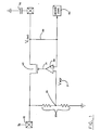
- Figure 1 is a circuit diagram of the preferred embodiment of the present invention.
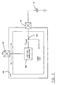
- Figure 2 is a simplified block diagram to graphically illustrate the placement of the present invention.
- Figure 3 is a circuit diagram of the op-amp used in connection with the preferred embodiment of the present invention.
- a voltage regulator is disclosed for use with on-board low operating supply voltage. While the following description makes reference to specific circuits, transistors, electronic elements, etc., it should be apparent to those skilled in the art that their equivalents are readily available for achieving the same objectives according to the present invention.
- N-well resistor divider 20 is connected to a typical 5 volt supply 10 to generate a 3.3 volt reference voltage Vref 31 at node 21.
- Vref 31 is also connected to reference input of op-amp 30.
- node 21, which is nominally at 3.3 volt can be adjusted to other levels of reference voltage for their intended purposes.
- Load voltage for device core 60 is at node 50, which is connected to the other input terminal of op-amp 30.
- the output 31 of op-amp 30 is connected to the gate of a P-channel field effect transistor ("PFET”) 40.
- PFET P-channel field effect transistor
- Capacitor 70 is "external" in that it is currently implemented outside of the integrated voltage regulator circuit, as is illustrated in Figure 2.
- Figure 2 is a graphical representation of voltage regulator 100 relative to external filter capacitor 120. While voltage regulator 100 supplies, via V-load 150, core 110, capacitor 120 is connected to V-load 150 through pin 121. A 5 volt power supply is drawn from pin 140, which can supply I/O strip 130. Accordingly, device core 110 can be operated at 3.3 volt, while the periphery and I/O operating at 5 volt.
- Vref 31 for op amp 30 is generated by N-well resistor divider 20 using 5 volt supply 10.
- V-load at node 50 is regulated by op-amp 30, which compares V-load at node 50 to match Vref 31 by turning ON and OFF PFET 40, which is a series dropping device, supplying the required current load to device core 60.
- PFET 40 as will be understood by those skilled in the art, is properly sized to suit the intended current load requirement.
- PFET 40 serves to control the current flow to node 50.
- V-load exceeds Vref 31
- op amp 30 turns ON and thus turning PFET 40 into the direction of OFF.
- V-load is below Vref 31
- the OFF state of op amp 30 turns PFET 40 in the direction of ON to supply the current load required for device core 60.
- External capacitor 70 is used for supplying transient current and filters load demand to avoid part failure due to VDD droop during switching. By implementing capacitor 70 externally, valuable silicon usage on the device can thus be optimized.
- Figure 3 is a circuit diagram of op amp 30 as it is currently implemented. It is a conventional circuit as will be appreciated by those skilled in the art.
Landscapes
- Engineering & Computer Science (AREA)
- Physics & Mathematics (AREA)
- Electromagnetism (AREA)
- General Physics & Mathematics (AREA)
- Radar, Positioning & Navigation (AREA)
- Automation & Control Theory (AREA)
- Microelectronics & Electronic Packaging (AREA)
- Continuous-Control Power Sources That Use Transistors (AREA)
Applications Claiming Priority (2)
| Application Number | Priority Date | Filing Date | Title |
|---|---|---|---|
| US14203593A | 1993-10-28 | 1993-10-28 | |
| US142035 | 1993-10-28 |
Publications (2)
| Publication Number | Publication Date |
|---|---|
| EP0651309A2 true EP0651309A2 (fr) | 1995-05-03 |
| EP0651309A3 EP0651309A3 (fr) | 1997-07-16 |
Family
ID=22498311
Family Applications (1)
| Application Number | Title | Priority Date | Filing Date |
|---|---|---|---|
| EP94114202A Withdrawn EP0651309A3 (fr) | 1993-10-28 | 1994-09-09 | Régulateur de tension CMOS embarqué. |
Country Status (2)
| Country | Link |
|---|---|
| EP (1) | EP0651309A3 (fr) |
| JP (1) | JPH07182053A (fr) |
Cited By (2)
| Publication number | Priority date | Publication date | Assignee | Title |
|---|---|---|---|---|
| EP0749059A3 (fr) * | 1995-06-14 | 1997-12-29 | Philips Patentverwaltung GmbH | Borne de contact de télécommunication avec régulateur de tension |
| FR2800936A1 (fr) * | 1999-11-10 | 2001-05-11 | Fujitsu Ltd | Circuit generateur de tension de reference |
Family Cites Families (5)
| Publication number | Priority date | Publication date | Assignee | Title |
|---|---|---|---|---|
| US4806844A (en) * | 1988-06-17 | 1989-02-21 | General Electric Company | Circuit for providing on-chip DC power supply in an integrated circuit |
| JPH087636B2 (ja) * | 1990-01-18 | 1996-01-29 | シャープ株式会社 | 半導体装置の電圧降下回路 |
| JP2888898B2 (ja) * | 1990-02-23 | 1999-05-10 | 株式会社日立製作所 | 半導体集積回路 |
| JPH04291608A (ja) * | 1991-03-20 | 1992-10-15 | Fujitsu Ltd | 電源回路 |
| US5168209A (en) * | 1991-06-14 | 1992-12-01 | Texas Instruments Incorporated | AC stabilization using a low frequency zero created by a small internal capacitor, such as in a low drop-out voltage regulator |
-
1994
- 1994-09-09 EP EP94114202A patent/EP0651309A3/fr not_active Withdrawn
- 1994-10-24 JP JP25816794A patent/JPH07182053A/ja not_active Withdrawn
Cited By (2)
| Publication number | Priority date | Publication date | Assignee | Title |
|---|---|---|---|---|
| EP0749059A3 (fr) * | 1995-06-14 | 1997-12-29 | Philips Patentverwaltung GmbH | Borne de contact de télécommunication avec régulateur de tension |
| FR2800936A1 (fr) * | 1999-11-10 | 2001-05-11 | Fujitsu Ltd | Circuit generateur de tension de reference |
Also Published As
| Publication number | Publication date |
|---|---|
| EP0651309A3 (fr) | 1997-07-16 |
| JPH07182053A (ja) | 1995-07-21 |
Similar Documents
| Publication | Publication Date | Title |
|---|---|---|
| USRE39374E1 (en) | Constant voltage power supply with normal and standby modes | |
| US7683592B2 (en) | Low dropout voltage regulator with switching output current boost circuit | |
| US5280198A (en) | Power supply level detector | |
| US7397227B2 (en) | Fast-disabled voltage regulator circuit with low-noise feedback loop and operating method thereof | |
| US7602162B2 (en) | Voltage regulator with over-current protection | |
| US5811993A (en) | Supply voltage independent bandgap based reference generator circuit for SOI/bulk CMOS technologies | |
| US20080203982A1 (en) | Power supply system for motherboard | |
| KR101774059B1 (ko) | 과도 부하 전압 조정기 | |
| US7626371B2 (en) | Power supply unit and portable device | |
| CN115777089B (zh) | 用于低压应用的低压差稳压器 | |
| EP1508078A2 (fr) | Regulateur de tension a courant de polarisation amplifie de fa on dynamique | |
| US6084385A (en) | System and method for multi-mode low power voltage regulator | |
| US20170220059A1 (en) | Regulator circuit | |
| CN100480943C (zh) | 电压调节器 | |
| US7227343B2 (en) | Linear voltage regulator with selectable output voltage | |
| CN115769166A (zh) | 基于电荷泵的低压差调节器 | |
| US20250044819A1 (en) | LDO/Band Gap Reference Circuit | |
| US5874830A (en) | Adaptively baised voltage regulator and operating method | |
| EP0651309A2 (fr) | Régulateur de tension CMOS embarqué | |
| US6885215B1 (en) | Voltage detector circuit with a programmable threshold point | |
| US20050242794A1 (en) | Voltage regulator | |
| US6737910B2 (en) | Semiconductor integrated circuit with constant internal power supply voltage | |
| US5483179A (en) | Data output drivers with pull-up devices | |
| US20240361790A1 (en) | Low-Power Floating-Rail Reference Generator | |
| CN112994221B (zh) | 一种芯片及电子设备 |
Legal Events
| Date | Code | Title | Description |
|---|---|---|---|
| PUAI | Public reference made under article 153(3) epc to a published international application that has entered the european phase |
Free format text: ORIGINAL CODE: 0009012 |
|
| AK | Designated contracting states |
Kind code of ref document: A2 Designated state(s): DE FR GB |
|
| PUAL | Search report despatched |
Free format text: ORIGINAL CODE: 0009013 |
|
| RHK1 | Main classification (correction) |
Ipc: G05F 1/46 |
|
| AK | Designated contracting states |
Kind code of ref document: A3 Designated state(s): DE FR GB |
|
| STAA | Information on the status of an ep patent application or granted ep patent |
Free format text: STATUS: THE APPLICATION IS DEEMED TO BE WITHDRAWN |
|
| 18D | Application deemed to be withdrawn |
Effective date: 19960330 |