EP0651403A2 - Magnetischer Film Fe-M-C und Herstellungsverfahren - Google Patents
Magnetischer Film Fe-M-C und Herstellungsverfahren Download PDFInfo
- Publication number
- EP0651403A2 EP0651403A2 EP94116628A EP94116628A EP0651403A2 EP 0651403 A2 EP0651403 A2 EP 0651403A2 EP 94116628 A EP94116628 A EP 94116628A EP 94116628 A EP94116628 A EP 94116628A EP 0651403 A2 EP0651403 A2 EP 0651403A2
- Authority
- EP
- European Patent Office
- Prior art keywords
- range
- magnetic film
- amorphous
- microclusters
- atomic
- Prior art date
- Legal status (The legal status is an assumption and is not a legal conclusion. Google has not performed a legal analysis and makes no representation as to the accuracy of the status listed.)
- Withdrawn
Links
Images



Classifications
-
- G—PHYSICS
- G11—INFORMATION STORAGE
- G11B—INFORMATION STORAGE BASED ON RELATIVE MOVEMENT BETWEEN RECORD CARRIER AND TRANSDUCER
- G11B5/00—Recording by magnetisation or demagnetisation of a record carrier; Reproducing by magnetic means; Record carriers therefor
- G11B5/127—Structure or manufacture of heads, e.g. inductive
- G11B5/31—Structure or manufacture of heads, e.g. inductive using thin films
- G11B5/3109—Details
-
- G—PHYSICS
- G11—INFORMATION STORAGE
- G11B—INFORMATION STORAGE BASED ON RELATIVE MOVEMENT BETWEEN RECORD CARRIER AND TRANSDUCER
- G11B5/00—Recording by magnetisation or demagnetisation of a record carrier; Reproducing by magnetic means; Record carriers therefor
- G11B5/127—Structure or manufacture of heads, e.g. inductive
- G11B5/147—Structure or manufacture of heads, e.g. inductive with cores being composed of metal sheets, i.e. laminated cores with cores composed of isolated magnetic layers, e.g. sheets
-
- H—ELECTRICITY
- H01—ELECTRIC ELEMENTS
- H01F—MAGNETS; INDUCTANCES; TRANSFORMERS; SELECTION OF MATERIALS FOR THEIR MAGNETIC PROPERTIES
- H01F10/00—Thin magnetic films, e.g. of one-domain structure
- H01F10/08—Thin magnetic films, e.g. of one-domain structure characterised by magnetic layers
- H01F10/10—Thin magnetic films, e.g. of one-domain structure characterised by magnetic layers characterised by the composition
- H01F10/12—Thin magnetic films, e.g. of one-domain structure characterised by magnetic layers characterised by the composition being metals or alloys
- H01F10/13—Amorphous metallic alloys, e.g. glassy metals
- H01F10/131—Amorphous metallic alloys, e.g. glassy metals containing iron or nickel
-
- H—ELECTRICITY
- H01—ELECTRIC ELEMENTS
- H01F—MAGNETS; INDUCTANCES; TRANSFORMERS; SELECTION OF MATERIALS FOR THEIR MAGNETIC PROPERTIES
- H01F17/00—Fixed inductances of the signal type
- H01F17/04—Fixed inductances of the signal type with magnetic core
-
- H—ELECTRICITY
- H01—ELECTRIC ELEMENTS
- H01F—MAGNETS; INDUCTANCES; TRANSFORMERS; SELECTION OF MATERIALS FOR THEIR MAGNETIC PROPERTIES
- H01F41/00—Apparatus or processes specially adapted for manufacturing or assembling magnets, inductances or transformers; Apparatus or processes specially adapted for manufacturing materials characterised by their magnetic properties
- H01F41/14—Apparatus or processes specially adapted for manufacturing or assembling magnets, inductances or transformers; Apparatus or processes specially adapted for manufacturing materials characterised by their magnetic properties for applying magnetic films to substrates
- H01F41/18—Apparatus or processes specially adapted for manufacturing or assembling magnets, inductances or transformers; Apparatus or processes specially adapted for manufacturing materials characterised by their magnetic properties for applying magnetic films to substrates by cathode sputtering
-
- H—ELECTRICITY
- H02—GENERATION; CONVERSION OR DISTRIBUTION OF ELECTRIC POWER
- H02K—DYNAMO-ELECTRIC MACHINES
- H02K99/00—Subject matter not provided for in other groups of this subclass
Definitions
- the present invention relates to an Fe-M-C magnetic film and a method of producing the same.
- this magnetic film is used as a magnetic head material for a VCR, a magnetic disk device or the like, as a core material for an ultramicro inductor contained in the inside of an integrated circuit or as a magnetic pole material for an ultramicro motor, or the like.
- such a conventional magnetic film has been produced, for example, by a thin-film forming technique such as sputtering, or the like, and used in the field of various information appliances such as a recording/reproducing head for a magnetic disk, and so on.
- a magnetic film for a magnetic head having high saturation magnetic flux density has been required so that recording can be made sufficiently in a recording medium of high coercive force.
- permeability is high and magnetostriction approaches a value near zero.
- durability against heat in heat treatment is high.
- an Fe-Al-Si alloy system (Sendust) and an amorphous alloy such as Co-Nb-Zr, Co-Ta-Zr, etc. have been developed and put into practical use (JP-A-60-74110).
- the saturation magnetic flux density is about 1 T and accordingly Sendust is not always satisfactory.
- the allowable temperature is about 500°C and accordingly the Co amorphous metal is not always sufficient to satisfy the conditions for the magnetic head producing process.
- microcrystalline clusters of Fe and TaC or microcrystalline clusters of Fe, TaC and Ta2C are formed (JP-A-03-131006, JP-A-03-132004 and JP-A-3-203307). Accordingly, annealing at least in conditions of 600°C and several hours has been required for stabilizing the fine microtexture structure of the crystalline clusters and stabilizing the magnetism thereof.
- the present invention is therefore intended to solve the aforementioned problem in the prior art.
- a first object of the present invention is to provide a magnetic film of an Fe-M-C system provided as a structure of high stability of the fine microtexture thereof and high stability of the magnetism thereof, without the necessity of long-term annealing at a high temperature and excellent in production efficiency and excellent so that the original magnetism of this system magnetic film can be fulfilled sufficiently.
- a second object of the present invention is to provide a method of producing such a magnetic film.
- a third object of the present invention is to provide a magnetic circuit element such as a magnetic head, or the like, using such a magnetic film.
- the inventors of the present application have made various experiments and examinations on the structure and magnetism of the Fe-M-C system magnetic film while making free use of the newest analyzing technique. As a result, there has been obtained a finding that a novel structure of the magnetic film capable of improving the stability of the magnetism thereof and the stability of the microtexture structure thereof is present in a specific composition.
- the present invention has been attained based on the finding, and the above-mentioned first object of the present invention is achieved by the following magnetic film.
- the magnetic film according to the present invention is characterized in that: the magnetic film has a composition composed of Fe, M and C as essential components, M representing at least one kind of metal selected from the group consisting of Ti, Zr, Hf, Nb, V, Ta, Mo, and W, Fe being in a range of from 65 atomic % to 80 atomic %, M being in a range of from 6 atomic % to 16 atomic % and C being residual atomic %; the magnetic film has a fine microtexture structure in which crystalline microclusters and amorphous microclusters are coexistent with each other, each of the crystalline microclusters having a body-centered cubic structure composed of the C atom and the Fe atom bonded thereto in an amount of from 3 % to 15 % and having a mean grain size of from 5 nm to 14 nm, each of the amorphous microclusters being composed of the M atom and the C atom and having a mean grain size of from 0.5 nm to 2
- the composition of respective constituent elements of the magnetic film elements partly common with the conventional magnetic film are contained in the magnetic film, but the two films extremely differ from each other in the microtexture structure constituting the film. That is, as described above, for example, in the case where the element M is Ta, the conventional magnetic film has a microtexture structure in which a crystal of TaC or Ta2C formed by bonding with C is coexistent with a crystal of Fe. On the contrary, in the case of the present invention, the element M (for example, Ta) is bonded with C atoms to form amorphous microclusters having a mean grain size of from 0. 5 nm to 2 nm.
- the magnetic film preferably has a composition composed of Fe in a range of from 65 atomic % to 80 atomic %, M in a range of from 6 % to 16 %, and C of residual atomic %, and more preferably has a composition composed of Fe in a range of from 72 atomic % to 79 atomic %, M in a range of from 8 % to 13 %, and C of residual atomic %. Further, more preferably, the magnetic film has a composition composed of Fe of 78 atomic %, M of 8.7 atomic %, and C of 13.3 atomic %.
- the mean grain size of the crystalline microclusters is smaller than 5 nm, the resulting magnetic film is undesirably inferior in soft magnetism. If the mean grain size is larger than 14 nm, the resulting magnetic film is undesirably large in magnetostriction.
- the means grain size of the crystalline microclusters is more preferably selected to be in a range of from 0.7 nm to 1.3 nm. Further, more preferably, the mean grain size thereof is selected to be 11.4 nm. If the rate of bonding of Fe atoms with C atoms is out of the range of from 3 % to 15 %, the resulting magnetic film is undesirably large in magnetostriction.
- the amorphous microclusters serve as a pinning material against the crystalline microclusters, that is, serve to control the crystal growth of the latter.
- the mean grain size of the amorphous microclusters is selected to be preferably in a rage of from 0.5 nm to 2 nm, more preferably, in a range of from 0.7 nm to 1.3 nm. If the mean grain size is smaller than 0.5 nm, the crystal growth of the crystalline microclusters cannot be suppressed more greatly than expected. If the mean grain size is larger than 14 nm, the crystal growth of the crystalline microclusters cannot be suppressed still more greatly than expected because of shortage of the number of grains. Further more preferably, the mean grain size of the amorphous microclusters is selected to be 0.9 nm.
- Conditions for annealing are not specifically limited as long as the crystalline microclusters and the amorphous microclusters can coexist with each other as described above when the amorphous film of a desired composition is annealed. According to the inventors' examination, it has been found that the crystalline microclusters and the amorphous microclusters are coexistent with each other as described above when the amorphous film is annealed at a temperature in a range of from 500°C to 560°C in an atmosphere of N2, that is, in a non-oxidative atmosphere for a time in a range of from 15 minutes to 60 minutes, preferably, for a time in a range of from 25 minutes to 30 minutes.
- the amorphous film is formed on a substrate by sputtering in the presence of a working gas with use of an alloy of a composition stoichiometrically coincident with a desired composition, for example, composed of Fe in a range of from 65 % to 80 %, M in a range of from 6 % to 16 %, and C of residual %, as a target.
- a working gas for example, composed of Fe in a range of from 65 % to 80 %, M in a range of from 6 % to 16 %, and C of residual %, as a target.
- the Fe-M-C alloy target may be replaced by an Fe-M alloy target and a CH4 gas of a predetermined partial pressure may be introduced as the C component.
- the pressure of the working gas at the time of sputtering is preferably selected to be higher than ordinary pressure (for example, 3 ⁇ 10 ⁇ 3 Pa) and in a range of from about 1 ⁇ 10 ⁇ 2 Pa to about 3 Pa.
- a substrate having a perovskite structure for example, a substrate having a perovskite structure is preferred. Typical examples thereof include NiO-containing CaTiO3 which is a nonmagnetic substrate.
- a magnetic substrate of spinel structure such as (Mn, Zn)Fe2O4 also can be used as the crystalline substrate. Accordingly, in the case where a magnetic head is to be produced by using the magnetic film, NiO-containing CaTiO3 which is a nonmagnetic substrate is preferably used.
- sputtering used in the present invention various known sputtering methods can be used.
- sputtering preferably used include RF bipolar sputtering, magnetron sputtering, bias sputtering, and so on.
- RF bipolar sputtering simple in the apparatus structure thereof and adapted for forming a uniform film on a broad substrate
- magnetron sputtering adapted for high-speed low-temperature conditions and so on. If the magnetic film formed by sputtering is annealed at a temperature of from 500°C to 560°C for a time of not larger than one hour, preferably, no larger than 30 minutes, the magnetic film can be annealed sufficiently.
- the atmosphere for annealing is, for example, selected to be a non-oxidative atmosphere such as an atmosphere of N2.
- the thickness of the magnetic film is selected suitably in accordance with the purpose of use and generally selected to be in a range of 2 ⁇ m to 20 ⁇ m.
- the third object is to provide a magnetic circuit element using this magnetic film.
- Typical application examples thereof include a magnetic head and a micro magnetic core, each of which is obtained by forming this magnetic film on a nonmagnetic substrate.
- the magnetic head is applied to a magnetic recording apparatus, and the micro magnetic core is applied to an inductor in an integrated circuit and further to an ultramicro motor.
- Fe atoms bonded with C atoms by an amount of from 3 % to 15 % form microclusters having a body-centered cubic structure ( ⁇ -Fe) and M atoms (for example, Ta atoms) and C atoms form amorphous microclusters to make the two kinds of microclusters coexistent with each other to thereby give the magnetic film an effect of suppressing the growth of the crystalline microclusters of Fe atoms against heat applied in a process of producing a magnetic head, or the like.
- ⁇ -Fe body-centered cubic structure
- M atoms for example, Ta atoms
- C atoms form amorphous microclusters to make the two kinds of microclusters coexistent with each other to thereby give the magnetic film an effect of suppressing the growth of the crystalline microclusters of Fe atoms against heat applied in a process of producing a magnetic head, or the like.
- C atoms in the microclusters of Fe atoms have an Fe3C (cementite) type local structure, so that the magnetostriction can be set to be almost zero ( ⁇ 0.000001) as a result of the coexistence of the fine crystal Fe atom micro clusters and the cementite type local structure.
- Fe atoms form crystalline microclusters having a body-centered cubic structure ( ⁇ -Fe)
- anisotropy of the structure is dispersed.
- the magnetocrystalline anisotropic effect is reduced, so that soft magnetism of high permeability and of low coercive force is obtained.
- the number of Fe atoms bonded with C atoms is small (from 3 % to 15 % of Fe), there is little reduction of magnetic moment of Fe. Accordingly, excellent magnetism is exhibited.
- the magnetic film formed by sputtering is annealed at a temperature of from 500°C to 560°C for a time of not larger than one hour, preferably, no larger than 30 minutes, the magnetic film can be annealed sufficiently. Accordingly, high-temperature long-term heat treatment has to be avoided. This is because the microtexture structure of the preferred magnetic film is destroyed so that the amorphous microcluster component formed by bonding of M atoms and C atoms is reduced.
- microtexture structure of an amorphous film and the technique of forming the amorphous film will be now described.
- An rf bipolar sputtering apparatus made by inventors to realize the embodiment was used for forming a magnetic film.
- film formation was performed by sputtering in the presence of a mixed gas of Ar (purity 99.9 %) and CH4 (purity 99.9 %) while using an alloy of Fe (purity 99.9 %) and Ta (purity 99.9 %) as a target.
- the composition of the film was controlled on the basis of the constituent atom proportion of the alloy target and the partial pressure of the CH4 gas.
- an amorphous film of a composition Fe 0.8 Ta 0.1 C 0.1 was formed on a perovskite substrate.
- the composition of the amorphous film formed in the aforementioned conditions was analyzed with an X-ray Micro Analyzer (XMA) (made by: Siemens A.G., type: SRS303 DA/WA).
- XMA X-ray Micro Analyzer
- the structure of the amorphous film was analyzed up to the atomic level with an X-ray diffractiometer (made by: philips, type: PW 1050/1390) and an Extended X-ray Absorption Fine Structure (EXAFS) measurement system (made by the inventors to realize the embodiment) using light emitted by a synchrotron (belongs to National Laboratory for High Energy Physics) as a light source.
- EXAFS Extended X-ray Absorption Fine Structure
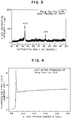
- Figs. 1 to 3 show measurement results of X-ray diffraction in the respective cases where CuK ⁇ X-rays were applied to three kinds of amorphous films formed as a composition Fe 0.8 Ta 0.1 C 0.1 on a nonmagnetic substrate, that is, an amorphous film just after film formation and amorphous films heat-treated in an atmosphere of N2 for 30 minutes at 500°C and 560°C respectively.
- the rate of heating from room temperature to 500°C or 560°C was 6.66°C/min
- the rates of cooling from 500°C or 560°C to room temperature were 3°C/min in a range of from 500°C or 560°C to 400°C, 2°C/min in a range of from 400°C to 200°C, and 1°C/min in a range of from 200°C to room temperature, respectively.
- used was an annealing apparatus formed by the inventors of the present invention by using an electric furnace made by Okura Riken Co., Ltd., and an electromagnet made by Tokin Corporation.
- Fig. 1 shows X-ray diffraction spectra just after film formation, which spectra show an amorphous structure exhibiting a broad scattering peak.
- Figs. 2 and 3 show only diffraction peaks of ⁇ -Fe crystal of a body-centered cubic structure.
- EXAFS Extended X-ray Absorption Fine Structure
- Fig. 4 shows measurement results of the fluorescent X-ray yield just after formation of the amorphous film Fe 0.8 Ta 0.1 C 0.1 .
- Spectra of the films heat-treated in an atmosphere of N2 for 30 minutes at 500°C and 560°C respectively are not shown in Fig. 4, because the apparent spectra thereof are substantially the same as the measurement results of the thin film just after film formation.
- the difference between the thus measured fluorescent X-ray yield spectra and fluorescent X-ray yield spectra on the assumption that Ta atoms stand alone is EXAFS ⁇ 0(k).
- the analysis of the structure of the amorphous material can be performed by analyzing this difference.
- F(R) obtained here is called a radial distribution function which expresses an electron density distribution in the distance of the radius R from the center atom and means the fact that an atom exists in the position of a local maximum.
- F(R) with respect to the fluorescent X-ray yield spectra functions as shown in Figs. 5 to 7 are obtained.
- Each of these is a radial distribution function with an Ta atom in the magnetic film of the composition Fe 0.8 Ta 0.1 C 0.1 as the center and expresses an amorphous material structure exhibiting broad scattering peaks besides the diffraction peaks of ⁇ -Fe crystal in X-ray diffraction.
- ⁇ C (k) ⁇ j N j f j (k)sin(2kR j + ⁇ j (k))exp(-2 ⁇ j k)/kR j (2)
- RF ⁇
- j represents a subscript expressing the kind of atoms in the vicinity of the X-ray absorption atom
- N j represents the number (coordination number) of j-kind atoms in the vicinity of the X-ray absorption atom
- f j represents the backscattering amplitude of the j-kind atoms for the electron wave
- R j represents the interatomic distance between the X-ray absorption atom and j-kind atoms in the vicinity of the X-ray absorption atom
- ⁇ j (k) represents a phase displacement caused by scattering of photoelectrons
- ⁇ j represents a Debye
- RF is a factor expressing coincidence between ⁇ 0(k) and ⁇ C (k). Parameters are set so that RF is minimized.
- f j and ⁇ j are parameters peculiar to each element
- R j , N j and ⁇ j are amorphous structure parameters determined by the least square method. The expression of the structure can be discussed mainly on the basis of the interatomic distance (R j ) and the coordination number (N j ).
- the respective coordination numbers of the samples (a), (b) and (c) were obtained on the basis of the coordination numbers of the reference samples (d) and (e) having known structures.
- R represents the interatomic distance
- N represents the coordination number
- the numerical value enclosed in parentheses represents the in-table deviation value of the last digit in each numerical value.
- the interatomic distance of the metal Ta crystal reference sample (sample d ) of the body-centered cubic structure and the interatomic distance of the TaC crystal reference sample (sample e ) of the face-centered cubic lattice NaCl type structure are coincident with values obtained by X-ray diffraction.
- the direct analyzed value is not coincident with the actual value because the C atoms are light-weighted elements so that the number of electrons scattering electron wave is small.
- the coordination number of Ta atoms in the film just after film formation is substantially coincident with a value obtained by multiplying the coordination number in the body-centered cubic by 0.8 corresponding to the composition of Fe atoms, so that there is no special condition in which clusters are formed.
- the Fe-Ta-C thin film according to the present invention does not contain crystal components of TaC and Ta2C though the film is heat-treated. From the analysis of the interatomic distance between Ta and Ta, there is inferred the structure in which Ta atoms form a cluster having a disorganized (amorphous) body-centered cubic structure in the thin film so that C atoms at the surface of the cluster are bonded with Fe atoms.
- Fig. 8 shows a structure model thereof.
- the number of constituent atoms of this cluster can be approximately obtained by analyzing the thin films heat-treated in an atmosphere of N2 at 500°C and 560°C respectively by an analyzing method which will be described later, and further, the size of the cluster can be obtained by supposing the amorphous body-centered cubic structure of Ta atoms.
- the size of the Ta atom cluster obtained in this manner is 0.5 nm diameter in the case of the thin film heat-treated at 500°C and 0.9 nm diameter in the case of the thin film heat-treated at 560°C. It is considered that such amorphous clusters are present between Fe fine crystal grains to prevent the ⁇ -Fe crystal from growing.
- Fig. 10 shows the ratio of the coordination number of Ta atoms to the coordination number of C atoms in the vicinity of Ta atoms, the ratio being expressed in a function of TaC cluster size.
- the thin film of the composition Fe 0.8 Ta 0.1 C 0.1 as a typical example has a structure in which the number of C atoms bonded with Ta is about 85 % and the residual C atoms of about 15 % are mixed in ⁇ -Fe crystal grains in the body-centered cubic structure constituted by Fe atoms or bonded with the surfaces of the ⁇ -Fe crystal grains.
- Ta-C amorphous clusters have a mean grain size of from 0.5 nm to 2 nm. Accordingly, ⁇ -Fe crystal grains have a mean grain size of from 10 nm to 14 nm in accordance with the composition and have a microtexture structure in which 3 % to 15 % of Fe atoms are bonded with C atoms. By giving such a structure, the growth of ⁇ -Fe crystal grains is suppressed so that good soft magnetism is obtained.
- the composition is out of the preferred range shown in Fig. 11, the crystal growth of ⁇ -Fe crystal grains cannot be suppressed by heat-treatment so that soft magnetism becomes poor because a large number of C atoms enter into the ⁇ -Fe crystal grains or the size of the Ta amorphous clusters is too small compared with the size of the ⁇ -Fe crystal grains.
- saturation magnetic flux density of 1.6 T is exhibited in the preferred region surrounded by the solid line in Fig. 11.
- Fig. 12 is a perspective view showing a head chip in a state in which a coil is removed.
- the reference numeral 1 designates a perovskite system nonmagnetic substrate; 2, Fe-Ta-C system magnetic films according to the present invention; 3, an SiO2 gap layer; 4, a chip having a window; 5, a chip having no window; and 6, a glass joint portion.
- a VCR magnetic head chip is formed through a process in which the Fe-Ta-C system magnetic films 2 having a thickness of from 15 ⁇ m to 20 ⁇ m is formed on the nonmagnetic substrate 1, the SiO2 gap layer 3 is formed, and then the chip 4 having a window and the chip 5 having no window are joined by glass to form the joint portion 6.
- the structure of the VCR magnetic head shown in this embodiment has been described as an example, and the present invention can be similarly applied also to other known devices, for example, to heads for magnetic recording apparatuses such as a magnetic disk device, etc., or the like, and the excellent characteristic of the magnetic film according to the present invention can be fulfilled.
- FIG. 13 and 14 are a perspective view of an important part thereof and a section thereof, respectively, the reference numeral 7 designates a circuit substrate; 8, an Fe-Ta-C system magnetic film according to the present invention; 9, a coil patterned on a circuit; and 10, an insulating protective film.
- a micro magnetic core By forming such a micro magnetic core on the LSI substrate 7, an inductor can be formed in the LSI circuit so that the formation of an integrated circuit functionally richer than the conventional integrated circuit can be performed.
- FIG. 15 is a partly enlarged perspective view of an important part thereof, the reference numeral 11 designates a circuit substrate; 12, magnetic cores obtained by using an Fe-Ta-C system magnetic film according to the present invention; 13, a coil patterned on a circuit; and 14, an insulating protective film.
- computer controlling requiring mechanical ultramicro displacement can be performed, for example, for the purpose of DNA cutting in the field of bioengineerings, or the like, so that high-precision controlling can be made in the wide field of ultramicro machining.
- the expected objects of the present invention could be achieved by the present invention. That is, not only the stability of magnetism and the stability of the microtexture structure of the film can be improved but also the heat-treatment conditions after film formation can be made low-temperature short-time conditions, so that a magnetic film excellent in production efficiency can be provided. Further, a method of producing the magnetic film can be provided as a simple method in which a target, a gas pressure and a substrate are set in specific conditions in accordance with conventional sputtering without necessity of any special complex process. Further, magnetic circuits of high performance can be provided by application of the magnetic film having excellent magnetism to various types of magnetic circuits.
Landscapes
- Engineering & Computer Science (AREA)
- Power Engineering (AREA)
- Manufacturing & Machinery (AREA)
- Microelectronics & Electronic Packaging (AREA)
- Thin Magnetic Films (AREA)
- Physical Vapour Deposition (AREA)
- Magnetic Heads (AREA)
- Coils Or Transformers For Communication (AREA)
- Permanent Magnet Type Synchronous Machine (AREA)
Applications Claiming Priority (2)
| Application Number | Priority Date | Filing Date | Title |
|---|---|---|---|
| JP5272438A JPH07130537A (ja) | 1993-10-29 | 1993-10-29 | Fe−M−C系磁性膜及び磁気回路素子 |
| JP272438/93 | 1993-10-29 |
Publications (2)
| Publication Number | Publication Date |
|---|---|
| EP0651403A2 true EP0651403A2 (de) | 1995-05-03 |
| EP0651403A3 EP0651403A3 (de) | 1995-09-13 |
Family
ID=17513922
Family Applications (1)
| Application Number | Title | Priority Date | Filing Date |
|---|---|---|---|
| EP94116628A Withdrawn EP0651403A3 (de) | 1993-10-29 | 1994-10-21 | Magnetischer Film Fe-M-C und Herstellungsverfahren. |
Country Status (3)
| Country | Link |
|---|---|
| EP (1) | EP0651403A3 (de) |
| JP (1) | JPH07130537A (de) |
| CN (1) | CN1079984C (de) |
Cited By (3)
| Publication number | Priority date | Publication date | Assignee | Title |
|---|---|---|---|---|
| DE19639428C2 (de) * | 1995-09-25 | 2002-06-20 | Alps Electric Co Ltd | Weichmagnetisches, dielektrisches Hochfrequenz-Verbundmaterial und Verfahren zu seiner Herstellung |
| CN113684450A (zh) * | 2021-08-24 | 2021-11-23 | 内蒙古大学 | 一种对小角度变化超敏感的薄膜及其制备方法和应用 |
| CN118529729A (zh) * | 2024-05-16 | 2024-08-23 | 北京理工大学 | 一种适用于2700℃以上极高温环境的材料及其制备方法 |
Families Citing this family (1)
| Publication number | Priority date | Publication date | Assignee | Title |
|---|---|---|---|---|
| CN105761878B (zh) * | 2016-04-29 | 2018-03-20 | 东南大学 | 一种Cu掺杂Fe‑N软磁薄膜及其制备方法 |
Family Cites Families (1)
| Publication number | Priority date | Publication date | Assignee | Title |
|---|---|---|---|---|
| JP2721562B2 (ja) * | 1989-03-08 | 1998-03-04 | アルプス電気株式会社 | 軟磁性合金膜 |
-
1993
- 1993-10-29 JP JP5272438A patent/JPH07130537A/ja active Pending
-
1994
- 1994-10-21 EP EP94116628A patent/EP0651403A3/de not_active Withdrawn
- 1994-10-28 CN CN94119335A patent/CN1079984C/zh not_active Expired - Fee Related
Cited By (3)
| Publication number | Priority date | Publication date | Assignee | Title |
|---|---|---|---|---|
| DE19639428C2 (de) * | 1995-09-25 | 2002-06-20 | Alps Electric Co Ltd | Weichmagnetisches, dielektrisches Hochfrequenz-Verbundmaterial und Verfahren zu seiner Herstellung |
| CN113684450A (zh) * | 2021-08-24 | 2021-11-23 | 内蒙古大学 | 一种对小角度变化超敏感的薄膜及其制备方法和应用 |
| CN118529729A (zh) * | 2024-05-16 | 2024-08-23 | 北京理工大学 | 一种适用于2700℃以上极高温环境的材料及其制备方法 |
Also Published As
| Publication number | Publication date |
|---|---|
| CN1109628A (zh) | 1995-10-04 |
| EP0651403A3 (de) | 1995-09-13 |
| JPH07130537A (ja) | 1995-05-19 |
| CN1079984C (zh) | 2002-02-27 |
Similar Documents
| Publication | Publication Date | Title |
|---|---|---|
| US6410170B1 (en) | High resistivity FeXN sputtered films for magnetic storage devices and method of fabrication | |
| EP0300511B1 (de) | Magnetkopf | |
| EP0584768B1 (de) | Herstellungsverfahren eines weichmagnetischen Filmes | |
| US5176806A (en) | Soft magnetic alloy film | |
| EP0238047B1 (de) | Magnetisches Speichermedium mit senkrechter Anisotropie | |
| Carey et al. | The magnetic and magneto‐optical properties of Co, Cr, Mn, and Ni substituted barium ferrite films | |
| EP0382195A1 (de) | Magnetkopf und Verfahren zu seiner Herstellung | |
| EP0466159B1 (de) | Zusammengesetzter Magnetkopf | |
| US5302469A (en) | Soft magnetic thin film | |
| JP3759191B2 (ja) | 薄膜磁気素子 | |
| EP0651403A2 (de) | Magnetischer Film Fe-M-C und Herstellungsverfahren | |
| EP0673021A1 (de) | Magnetische Aufzeichnungsmedium sowie Verfahren zu seiner Herstellung | |
| EP0253282B1 (de) | Dünner Film mit grossem Kerr-Rotationswinkel und Verfahren zu seiner Herstellung | |
| TWI400698B (zh) | 合金的序化方法及其垂直記錄媒體的製作方法 | |
| EP0418804B1 (de) | Dünner weichmagnetischer Film | |
| EP0298840B1 (de) | Magnetischer Aufzeichnungsträger und dessen Herstellungsverfahren | |
| JP2003100515A (ja) | 高飽和磁化を有する磁心用軟磁性薄膜 | |
| JPS63106916A (ja) | 磁気記録媒体 | |
| JP2996553B2 (ja) | 軟磁性合金薄膜 | |
| JPH0669032A (ja) | 積層磁性薄膜およびそれを用いた磁気ヘッド | |
| JP2935606B2 (ja) | 磁気ディスクの製造方法 | |
| EP0522982B1 (de) | Auf FeGaSi basiertes magnetisches Material mit Ir als Zusatz | |
| JPH05271885A (ja) | 軟磁性合金薄膜およびその製造方法 | |
| JPH09306736A (ja) | 垂直磁化膜およびその製造法ならびに 光磁気記録媒体 | |
| JPH0636928A (ja) | 軟磁性材料 |
Legal Events
| Date | Code | Title | Description |
|---|---|---|---|
| PUAI | Public reference made under article 153(3) epc to a published international application that has entered the european phase |
Free format text: ORIGINAL CODE: 0009012 |
|
| 17P | Request for examination filed |
Effective date: 19941021 |
|
| AK | Designated contracting states |
Kind code of ref document: A2 Designated state(s): DE FR GB |
|
| PUAL | Search report despatched |
Free format text: ORIGINAL CODE: 0009013 |
|
| AK | Designated contracting states |
Kind code of ref document: A3 Designated state(s): DE FR GB |
|
| 17Q | First examination report despatched |
Effective date: 19990519 |
|
| STAA | Information on the status of an ep patent application or granted ep patent |
Free format text: STATUS: THE APPLICATION IS DEEMED TO BE WITHDRAWN |
|
| 18D | Application deemed to be withdrawn |
Effective date: 19991230 |