EP0652455A1 - Anordnung von gesteuerten Dünnschichtspiegeln für ein optisches Projektionssystem und Verfahren zu deren Herstellung - Google Patents
Anordnung von gesteuerten Dünnschichtspiegeln für ein optisches Projektionssystem und Verfahren zu deren Herstellung Download PDFInfo
- Publication number
- EP0652455A1 EP0652455A1 EP94117538A EP94117538A EP0652455A1 EP 0652455 A1 EP0652455 A1 EP 0652455A1 EP 94117538 A EP94117538 A EP 94117538A EP 94117538 A EP94117538 A EP 94117538A EP 0652455 A1 EP0652455 A1 EP 0652455A1
- Authority
- EP
- European Patent Office
- Prior art keywords
- layer
- thin film
- array
- motion
- inducing
- Prior art date
- Legal status (The legal status is an assumption and is not a legal conclusion. Google has not performed a legal analysis and makes no representation as to the accuracy of the status listed.)
- Granted
Links
- 239000010409 thin film Substances 0.000 title claims abstract description 130
- 230000003287 optical effect Effects 0.000 title claims abstract description 18
- 238000000034 method Methods 0.000 title claims description 54
- 238000004519 manufacturing process Methods 0.000 title claims description 17
- 230000001939 inductive effect Effects 0.000 claims abstract description 72
- 125000006850 spacer group Chemical group 0.000 claims abstract description 50
- 239000011159 matrix material Substances 0.000 claims abstract description 30
- 239000000463 material Substances 0.000 claims abstract description 20
- 239000000919 ceramic Substances 0.000 claims description 25
- 238000005530 etching Methods 0.000 claims description 11
- 238000000151 deposition Methods 0.000 claims description 10
- 238000004544 sputter deposition Methods 0.000 claims description 10
- 229910052751 metal Inorganic materials 0.000 claims description 9
- 239000002184 metal Substances 0.000 claims description 9
- 239000000758 substrate Substances 0.000 claims description 8
- 239000004020 conductor Substances 0.000 claims description 5
- 229920000642 polymer Polymers 0.000 claims description 5
- 238000005229 chemical vapour deposition Methods 0.000 claims description 4
- 230000004044 response Effects 0.000 claims description 3
- NJPPVKZQTLUDBO-UHFFFAOYSA-N novaluron Chemical compound C1=C(Cl)C(OC(F)(F)C(OC(F)(F)F)F)=CC=C1NC(=O)NC(=O)C1=C(F)C=CC=C1F NJPPVKZQTLUDBO-UHFFFAOYSA-N 0.000 claims description 2
- 238000003980 solgel method Methods 0.000 claims 1
- 230000005684 electric field Effects 0.000 description 14
- 230000008569 process Effects 0.000 description 4
- 239000010931 gold Substances 0.000 description 3
- 239000000126 substance Substances 0.000 description 3
- -1 e.g. Substances 0.000 description 2
- BQCADISMDOOEFD-UHFFFAOYSA-N Silver Chemical compound [Ag] BQCADISMDOOEFD-UHFFFAOYSA-N 0.000 description 1
- 229910052782 aluminium Inorganic materials 0.000 description 1
- XAGFODPZIPBFFR-UHFFFAOYSA-N aluminium Chemical compound [Al] XAGFODPZIPBFFR-UHFFFAOYSA-N 0.000 description 1
- 230000008020 evaporation Effects 0.000 description 1
- 238000001704 evaporation Methods 0.000 description 1
- PCHJSUWPFVWCPO-UHFFFAOYSA-N gold Chemical compound [Au] PCHJSUWPFVWCPO-UHFFFAOYSA-N 0.000 description 1
- 229910052737 gold Inorganic materials 0.000 description 1
- HFGPZNIAWCZYJU-UHFFFAOYSA-N lead zirconate titanate Chemical compound [O-2].[O-2].[O-2].[O-2].[O-2].[Ti+4].[Zr+4].[Pb+2] HFGPZNIAWCZYJU-UHFFFAOYSA-N 0.000 description 1
- 238000005459 micromachining Methods 0.000 description 1
- 230000004048 modification Effects 0.000 description 1
- 238000012986 modification Methods 0.000 description 1
- 230000010287 polarization Effects 0.000 description 1
- 238000002360 preparation method Methods 0.000 description 1
- 239000004065 semiconductor Substances 0.000 description 1
- 229910052709 silver Inorganic materials 0.000 description 1
- 239000004332 silver Substances 0.000 description 1
- 238000004513 sizing Methods 0.000 description 1
- 229910052721 tungsten Inorganic materials 0.000 description 1
- WFKWXMTUELFFGS-UHFFFAOYSA-N tungsten Chemical compound [W] WFKWXMTUELFFGS-UHFFFAOYSA-N 0.000 description 1
- 239000010937 tungsten Substances 0.000 description 1
Images




Classifications
-
- H—ELECTRICITY
- H04—ELECTRIC COMMUNICATION TECHNIQUE
- H04N—PICTORIAL COMMUNICATION, e.g. TELEVISION
- H04N9/00—Details of colour television systems
- H04N9/12—Picture reproducers
- H04N9/30—Picture reproducers using solid-state colour display devices
-
- G—PHYSICS
- G02—OPTICS
- G02B—OPTICAL ELEMENTS, SYSTEMS OR APPARATUS
- G02B26/00—Optical devices or arrangements for the control of light using movable or deformable optical elements
- G02B26/08—Optical devices or arrangements for the control of light using movable or deformable optical elements for controlling the direction of light
- G02B26/0816—Optical devices or arrangements for the control of light using movable or deformable optical elements for controlling the direction of light by means of one or more reflecting elements
- G02B26/0833—Optical devices or arrangements for the control of light using movable or deformable optical elements for controlling the direction of light by means of one or more reflecting elements the reflecting element being a micromechanical device, e.g. a MEMS mirror, DMD
- G02B26/0858—Optical devices or arrangements for the control of light using movable or deformable optical elements for controlling the direction of light by means of one or more reflecting elements the reflecting element being a micromechanical device, e.g. a MEMS mirror, DMD the reflecting means being moved or deformed by piezoelectric means
-
- Y—GENERAL TAGGING OF NEW TECHNOLOGICAL DEVELOPMENTS; GENERAL TAGGING OF CROSS-SECTIONAL TECHNOLOGIES SPANNING OVER SEVERAL SECTIONS OF THE IPC; TECHNICAL SUBJECTS COVERED BY FORMER USPC CROSS-REFERENCE ART COLLECTIONS [XRACs] AND DIGESTS
- Y10—TECHNICAL SUBJECTS COVERED BY FORMER USPC
- Y10S—TECHNICAL SUBJECTS COVERED BY FORMER USPC CROSS-REFERENCE ART COLLECTIONS [XRACs] AND DIGESTS
- Y10S359/00—Optical: systems and elements
- Y10S359/904—Micromirror
Definitions
- the present invention relates to an optical projection system; and, more particularly, to an array of M x N thin film actuated mirrors for use in the system and method for the manufacture thereof.
- an optical projection system is known to be capable of providing a high quality display in a large scale.
- light from a lamp is uniformly illuminated onto an array of, e.g., M x N, actuated mirrors such that each of the mirrors is coupled with each of the actuators.
- the actuators may be made of an electrodisplacive material such as a piezoelectric or an electrostrictive material which deforms in response to an electric field applied thereto.
- the reflected light beam from each of the mirrors is incident upon an aperture of a baffle.
- an electrical signal to each of the actuators By applying an electrical signal to each of the actuators, the relative position of each of the mirrors to the incident light beam is altered, thereby causing a deviation in the optical path of the reflected beam from each of the mirrors.
- the optical path of each of the reflected beams is varied, the amount of light reflected from each of the mirrors which passes through the aperture is changed, thereby modulating the intensity of the beam.
- the modulated beams through the aperture are transmitted onto a projection screen via an appropriate optical device such as a projection lens, to thereby display an image thereon.
- FIG. 1 there is shown a cross sectional view of an M x N electrodisplacive actuated mirror array 10 for use in an optical projection system, disclosed in a copending commonly owned application, U.S. Ser. No. 08/278,660 , entitled "ELECTRODISPLACIVE ACTUATED MIRROR ARRAY, comprising: an active matrix 11 including a substrate 12 and an array of M x N transistors thereon; an array 13 of M x N electrodisplacive actuators 30, each of the electrodisplacive actuators 30 including a pair of actuating members 14, 15, a pair of bias electrodes 16, 17, and a common signal electrode 18; an array 19 of M x N hinges 31, each of the hinges 31 fitted in each of the electrodisplacive actuators 30; an array 20 of M x N connecting terminals 22, each of the connecting terminals 22 being used for electrically connecting each of the signal electrodes 18 with the active matrix 11; and an array 21 of M x N mirrors 23, each of the mirrors 23 being mounted on top of each of the
- a primary object of the present invention is to provide a method for manufacturing an array of M x N actuated mirrors, which dispenses with the use of a thin electrodiplacive ceramic wafer.
- an array of M x N thin film actuated mirrors for use in an optical projection system, the array comprising: an active matrix including a substrate, an array of M x N transistors and an array of M x N connecting terminals; an array of M x N thin film actuating structures, each of the actuating structures being provided with a top and a bottom surfaces, a proximal and a distal ends, each of the actuating structures including at least a thin film layer of a motion-inducing material having a top and bottom surfaces, and a first and a second electrodes with the first electrode being placed on the top surface of the motion-inducing layer and the second electrode, on the bottom surface of the motion-inducing layer, wherein an electrical signal applied across the motion-inducing layer between the first and second electrodes causes a deformation of the motion-inducing layer, and hence the actuating structure; an array of M x N supporting members, each of the supporting members being provided with
- a novel method for manufacturing an array of M x N actuated mirrors for use in an optical projection system comprising the steps of: (a) providing an active matrix having a top and a bottom surfaces, the active matrix including a substrate, an array of M x N transistors and an array of M x N connecting terminals; (b) forming a first supporting layer on the top surface of the active matrix, the first supporting layer including an array of M x N pedestals corresponding to the array of M x N supporting members in the array of M x N thin film actuated mirrors and a first sacrificial area; (c) treating the first sacrificial area of the first supporting layer to be removable; (d) depositing a first thin film electrode layer on the first supporting layer; (e)providing a thin film motion-inducing layer on the first thin film electrode layer; (f) forming a second thin film electrode layer on the thin film motion-in
- FIGs. 2 to 10 there are provided schematic cross sectional views of the inventive array of M x N thin film actuated mirrors for use in an optical projection system and method for the manufacture thereof, wherein M and N are integers, in accordance with preferred embodiments of the present invention. It should be noted that like parts appearing in Figs. 2 to 10 are represented by like reference numerals.
- FIG. 2 there is illustrated a cross sectional view of a first embodiment of an array 50 of M x N thin film actuated mirrors 51, comprising an active matrix 52, an array 53 of M x N thin film actuating structures 54, an array 55 of M x N supporting members 56, an array 57 of M x N spacer members 58 and an array 59 of M x N mirror layers 60.
- Fig. 3 represents a detailed cross sectional view of the thin film actuated mirror array 50 shown in Fig. 2.
- the active matrix 52 includes a substrate 59, an array of M x N transistors (not shown) and an array 61 of M x N connecting terminals 62.
- Each of the actuating structures 54 is provided with a top and a bottom surfaces 63, 64, a proximal and a distal ends, 65, 66, and further includes at least a thin film layer 67 of a motion inducing material having a top and a bottom surfaces 68, 69 and a first and second electrodes 70, 71, made of, e.g., a metal such as gold (Au) or silver (Ag), the first electrode 70 having a top surface 72.
- the first electrode 70 is placed on the top surface 68 of the motion-inducing thin film layer 67 and the second electrode 71, on the bottom surface 69 thereof.
- the motion-inducing thin film layer 67 is made of a piezoelectric ceramic, an electrostrictive ceramic, a magnetrostrictive ceramic or a piezoelectric polymer. In the case when the motion-inducing thin film layer 67 is made of a piezoelectric ceramic or a piezoelectric polymer, it must be poled.
- Each of the M x N supporting members 56 is used for holding each of the actuating structures 54 in place and also for electrically connecting the second electrode 71 in each of the actuating structures 54 with the corresponding connecting terminals 62 on the active matrix 52 by being provided with a conduit 118 made of an electrically conductive material, e.g., a metal.
- each of the actuating structures 54 is cantilevered from each of the supporting members 56 by being mounted on the top surface 73 of each of the supporting members 56 at the bottom surface 64 of each of the actuating structures 54 at the proximal end 65 thereof, and the bottom surface 74 of each of the supporting members 56 is placed on top of the active matrix 52.
- Each of the spacer members 58 provided with a top and a bottom surfaces 75, 76, is placed on the top surface 63 of each of the actuating structures 54 at the distal end 66 thereof.
- each of the mirror layers 60 including a mirror 77 for reflecting light beams, a supporting layer 78, having a top surface 81, a first and a second portions 79, 80 corresponding to the distal and proximal ends 66, 65 of each of the actuating structures 54, respectively, wherein the first portion 79 of each of the mirror layers 60 secured to the top surface 75 of each of spacer members 58 and the second portion 80 is cantilevered from each of the supporting members 56.
- the mirror 77 is placed on the top surface 81 of the supporting layer 78.
- each of the thin film actuated mirrors 51 can be further provided with an elastic layer 88.
- the elastic layer 88 can be placed either intermodiate the spacer member 58 and the first electrode 70 or on bottom of the second electrode 71 in each of the actuated mirrors 51.
- Fig. 4 a thin film actuated mirror 51 provided with an elastic layer 88 on the bottom surface 64 of the actuating structure 54.
- the material making up the supporting layer 78 in each of the mirror layers 60 can be also light reflecting, e.g., aluminum (Al), which will allow the top surface 81 thereof to function also as the mirror 77 in each of the thin film actuated mirrors 51, as depicted in Fig. 5.
- Al aluminum
- the inventive array 50 of thin film actuated mirrors 51 can function equally well by having the top and bottom surfaces 68, 69 of the motion-inducing thin film layer 67 in each of the actuating structures 54 covered completely with the first and second electrodes 70, 71 or by having either one of the top and bottom surfaces 68, 69 of the motion-inducing thin film layer 67 in each of the actuating structures 54 covered partially with the first and second electrodes 70, 71.
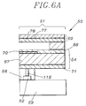
- the thin film actuated mirror 51 must be provided with an elastic layer 88. Two examples of the thin film actuated mirror 51 having such a structure are illustrated in Figs. 6A and 6B.
- FIGs. 3 and 7 an array 50 of M x N thin film actuated mirrors 51 comprising an array of M x N actuating structures 54, made of a piezoelectric ceramic, e.g., lead zirconium titanate(PZT).
- An electric field is applied across the motion-inducing thin film piezoelectric layer 67 located between the first and second electrodes 70, 71 in each of the actuating structured 54.
- the application of the electric field will either cause the piezoelectric ceramic to contract or expand, depending on the polarity of the electric field with respect to the poling of the piezoelectric material.
- the piezoelectric ceramic will contract. If the polarity of the electric field is opposite the polarity of the piezoelectric ceramic, the piezoelectric ceramic will expand.
- the polarity of the piezoelectric ceramic corresponds to the polarity of the applied electric field, causing the piezoelectric ceramic to contract.
- the actuating structure 54 bends downward, as shown in Fig. 7, thereby tilting the mirror layer 60 downward at an angle.
- the mirror layer 60 remains planar, and as a result, the effective length of the mirror layer 60 is the entire length of the mirror layer 60.
- the portion of the mirror layer 60 secured to the supporting member 56 does not deform in reaction to the electric field, but remains securely in place.
- the effective length of the mirror layer 60 is equal to a length less the length of the portion of the actuating structure 54 secured to the supporting member 56.
- Figs. 3 and 7 it can be shown that the light impinging on the mirror layer 60, of the actuated mirror 51 shown in Fig. 7 is deflected at a larger angle than the light reflected from of the unactuated actuated mirror 51 shown in Fig. 3.
- an electric field of a reverse polarity may be applied across the motion-inducing thin film piezoelectric layer 67, causing the piezoelectric ceramic to expand.
- the actuating structure 54 bends upward(not shown). The light impinging the mirror layer 60 of the upwardly actuated mirror 51 is deflected at a smaller angle than the light deflected from the unactuated actuated mirror 51 shown in Fig. 3.
- FIG. 8 a cross sectional view of a second embodiment of an array 100 of M x N thin film actuated mirrors 101, wherein the second embodiment is similar to the first embodiment except that each of the actuating structures 54 is of a bimorph structure, including a first electrode 70, a second electrode 71, an intermediate metal layers 87 an upper motion-inducing thin film layer 89 having a top and a bottom surfaces 90, 91 and a lower motion-inducing thin film layer 92 provided with a top and bottom surfaces 93, 94.
- the upper and lower motion-inducing thin film layers 89,92 are separated by the intermediate metal layer 87, the first electrode 70 placed on the top surface 90 of the upper motion-inducing thin film layer 89, and the second electrode 71, on the bottom surface 94 of the lower motion-inducing thin film layer 92.
- the upper and lower motion-inducing thin film layers 89, 92 in each of the actuating structures 54 are made of a piezoelectric ceramic, an electrostrictive ceramic, a magnetostrictive ceramic or a piezoelectric polymer.
- the upper and lower motion-inducing thin film layers 89,92 are made of a piezoelectric ceramic or a piezoelectric polymer, the upper and lower motion-inducing thin film layers 89,92 must be poled in such a way that the polarization direction of piezoelectric material in the upper motion-inducing thin film layer 89 is opposite from that of the lower motion-inducing thin film layer 92.
- the upper and lower motion-inducing layers 89, 90 in the array 100 of M x N thin film actuated mirrors 101 shown in Fig. 8 are made of a piezoelectric ceramic, e.g., PZT.
- PZT piezoelectric ceramic
- the actuating structure 54 will bend upward. In this situation, the impinging light is deflected at a smaller angle from the actuating structure 54 than the deflected light from the unactuated actuating structure 54. However, if the polarity of the piezoelectric ceramic and the electric field causes the upper motion-inducing thin film piezoelectric layer 89 to expand and the lower motion-inducing thin film piezoelectric layer 92 to contract, the actuating structure 54 will bend downward. In this situation, the impinging light is deflected at a larger angle from the actuating structure 54 than the deflected light from the unactuated actuating structure 54.
- FIG. 9 a cross sectional view of a third embodiment of an array 200 of M x N thin film actuated mirror 201, wherein the third embodiment is similar to the first embodiment except that the array 57 of M x N spacer members is absent. Instead, in each of the thin film actuated mirrors 51, the supporting layer 78 is simultaneousely connected to the distal end 66 of the actuating structure 54 and to the active matrix 52.
- Figs. 10A to 10I the manufacturing steps involved in manufacturing of the first embodiment of the present invention.
- the process for manufacturing the first embodiment i.e., the array 50 of M x N thin film actuated mirror 51, wherein M x N are integers, begins with the preparation of the active matrix 52, having the top and a bottom surfaces 102, 103, comprising the substrate 59, the array of M x N transistors (not shown) and the array 104 of M x N connecting terminals 105, as illustrated in Fig. 10A.
- a first supporting layer 106 including an array 107 of M x N pedestals 108 corresponding to the array 55 of M x N supporting members 56 and a first sacrificial area 109, wherein the first supporting layer 106 is formed by: depositing a sacrificial layer (not shown) on the entirety of the top surface 102 of the active matrix 52; forming an array of M x N empty slots (not shown), to thereby generated the first sacrificial area 109, each of the empty slots being located around each of the M x N connecting terminals 62; and providing a pedestal 108 in each of the empty slots, as shown in Fig. 10B.
- the sacrificial layer is formed by using a sputtering method, the array of empty slots, using an etching method, and the pedestals, using a sputtering or a chemical vapor deposition(CVD) method, followed by an etching method.
- the sacrificial area 109 of the first supporting layer 106 is then treated so as to be removable later using an etching method or the application of chemicals.
- an electrically conductive material e.g., tungsten(W)
- a first thin film electrode layer 111 made of an electrically conducting material, e.g., Au, is deposited on the first supporting layer 106.
- a thin film motion-inducing layer 112, made of a motion-inducing material, e.g., PZT, and a second thin film electrode layer 113 are then respectively formed on the first thin film electrode layer 111.
- a spacer layer 114 is provided on top of the second thin film electrode layer 111, the spacer layer 114 including the array 57 of M x N spacer members 58 and a second sacrificial area 115, as depicted in Fig. 10E.
- the method used in forming the spacer layer 114 is similar to the one used in forming the first supporting layer 106.
- the second sacrificial area 115 of the spacer layer 114 is then treated so as to be removable.
- a second supporting layer 116 and a light reflecting layer 117 comprising the mirror layer 60 are successively deposited on top of the spacer layer 114, as shown in Fig. 10F.
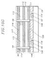
- the thin film layers of the electrically conducting, the motion-inducing, and the light reflecting materials may be deposited and patterned with the known thin film techniques, such as sputtering, sol-gel, evaporation, etching and micro-machining, as shown in Fig. 10G.
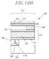
- the first and second sacrificial areas 109, 115 of the supporting layer 106 and the spacer layer 114 are then removed or dissolved by the application of chemical to thereby form said array 50 of M x N thin film actuated mirrors 51, as illustrated in Fig. 10H.
- the second embodiment is fabricated in a similar manner as the first embodiment.
- the first supporting layer is applied to the active matrix.
- the first supporting layer also includes the array of M x N pedestals corresponding to the array of M x N supporting members and the sacrificial area.
- the first thin film electrode layer, the lower thin film motion-inducing layer, the intermediate metal layer, the upper thin film motion-inducing layer, and the second thin film electrode layer are then deposited respectively on the first supporting layer.
- the spacer and mirror layers are successively formed.
- the thin film layers of an electrically conducting, a motion-inducing and a light reflecting materials are deposited and patterned with the known thin film techniques, as stated earlier.
- the sacrificial areas of the first supporting and spacer layers are next dissolved or removed by the application of a chemical, leaving the array 100 of thin film actuated mirrors 101, having the array 53 of M x N actuating structures 54 with the bimorph structure.
- an additional process for forming the elastic layer 88 can be added, involving a similar process as in the forming of other thin film layers.
Landscapes
- Physics & Mathematics (AREA)
- Engineering & Computer Science (AREA)
- Multimedia (AREA)
- Signal Processing (AREA)
- General Physics & Mathematics (AREA)
- Optics & Photonics (AREA)
- Mechanical Light Control Or Optical Switches (AREA)
- Optical Elements Other Than Lenses (AREA)
- Transforming Electric Information Into Light Information (AREA)
- Micromachines (AREA)
Applications Claiming Priority (6)
| Application Number | Priority Date | Filing Date | Title |
|---|---|---|---|
| KR1019930023725A KR970006686B1 (ko) | 1993-11-09 | 1993-11-09 | 광로조절장치 |
| KR1019930023726A KR970006687B1 (ko) | 1993-11-09 | 1993-11-09 | 광로조절장치 |
| KR9323725 | 1993-11-09 | ||
| KR9323726 | 1993-11-09 | ||
| KR93025877A KR970006696B1 (en) | 1993-11-30 | 1993-11-30 | A manufacturing method for an optical path regulating apparatus |
| KR9325877 | 1993-11-30 |
Publications (2)
| Publication Number | Publication Date |
|---|---|
| EP0652455A1 true EP0652455A1 (de) | 1995-05-10 |
| EP0652455B1 EP0652455B1 (de) | 1999-09-15 |
Family
ID=27349015
Family Applications (1)
| Application Number | Title | Priority Date | Filing Date |
|---|---|---|---|
| EP94117538A Expired - Lifetime EP0652455B1 (de) | 1993-11-09 | 1994-11-07 | Anordnung von gesteuerten Dünnschichtspiegeln für ein optisches Projektionssystem und Verfahren zu deren Herstellung |
Country Status (16)
| Country | Link |
|---|---|
| US (1) | US5760947A (de) |
| EP (1) | EP0652455B1 (de) |
| JP (1) | JP3165444B2 (de) |
| CN (1) | CN1047903C (de) |
| AU (1) | AU693125B2 (de) |
| BR (1) | BR9408009A (de) |
| CA (1) | CA2176111A1 (de) |
| CZ (1) | CZ290728B6 (de) |
| DE (1) | DE69420669T2 (de) |
| ES (1) | ES2140492T3 (de) |
| HU (1) | HU220517B1 (de) |
| IT (1) | IT1271708B (de) |
| PL (1) | PL176490B1 (de) |
| RU (1) | RU2141175C1 (de) |
| TW (1) | TW279931B (de) |
| WO (1) | WO1995013683A1 (de) |
Cited By (7)
| Publication number | Priority date | Publication date | Assignee | Title |
|---|---|---|---|---|
| EP0718658A1 (de) * | 1994-12-19 | 1996-06-26 | Daewoo Electronics Co., Ltd | Bei niedriger Temperatur hergestellte Matrix aus verstellbaren Dünnfilm-Spiegeln |
| GB2304424A (en) * | 1995-08-22 | 1997-03-19 | Daewoo Electronics Co Ltd | Thin film actuated mirror |
| GB2304918A (en) * | 1995-08-30 | 1997-03-26 | Daewoo Electronics Co Ltd | Tin film actuated mirror |
| GB2314939A (en) * | 1996-06-29 | 1998-01-14 | Daewoo Electronics Co Ltd | Thin film actuated mirror array having an increased tilt angle. |
| WO1998008127A1 (en) * | 1996-08-21 | 1998-02-26 | Daewoo Electronics Co., Ltd. | Thin film actuated mirror array for use in an optical projection system |
| CN1104815C (zh) * | 1996-01-31 | 2003-04-02 | 大宇电子株式会社 | 具有介质层的薄膜可驱动反射镜阵列 |
| EP1237205A3 (de) * | 2001-03-02 | 2005-02-09 | Ngk Insulators, Ltd. | Piezoelektrisches/elektrostriktives Bauelement zur Lichtreflexion sowie dessen Herstellungsverfahren |
Families Citing this family (22)
| Publication number | Priority date | Publication date | Assignee | Title |
|---|---|---|---|---|
| US5930025A (en) * | 1996-05-29 | 1999-07-27 | Daewoo Electronics Co., Ltd. | Array of thin film actuated mirrors and method for the manufacture thereof |
| KR100229788B1 (ko) * | 1996-05-29 | 1999-11-15 | 전주범 | 광로 조절 장치의 제조 방법 |
| KR980003662A (ko) * | 1996-06-28 | 1998-03-30 | 배순훈 | 큰 구동 각도를 가지는 박막형 광로 조절 장치 |
| US5898515A (en) * | 1996-11-21 | 1999-04-27 | Eastman Kodak Company | Light reflecting micromachined cantilever |
| US5949568A (en) * | 1996-12-30 | 1999-09-07 | Daewoo Electronics Co., Ltd. | Array of thin film actuated mirrors having a levelling member |
| US5914803A (en) * | 1997-07-01 | 1999-06-22 | Daewoo Electronics Co., Ltd. | Thin film actuated mirror array in an optical projection system and method for manufacturing the same |
| US6028690A (en) * | 1997-11-26 | 2000-02-22 | Texas Instruments Incorporated | Reduced micromirror mirror gaps for improved contrast ratio |
| US5920421A (en) * | 1997-12-10 | 1999-07-06 | Daewoo Electronics Co., Ltd. | Thin film actuated mirror array in an optical projection system and method for manufacturing the same |
| US6404942B1 (en) | 1998-10-23 | 2002-06-11 | Corning Incorporated | Fluid-encapsulated MEMS optical switch |
| US6389189B1 (en) | 1998-10-23 | 2002-05-14 | Corning Incorporated | Fluid-encapsulated MEMS optical switch |
| JP2000194282A (ja) * | 1998-12-24 | 2000-07-14 | Daewoo Electronics Co Ltd | 映像ディスプレーシステム |
| US6643426B1 (en) | 1999-10-19 | 2003-11-04 | Corning Incorporated | Mechanically assisted release for MEMS optical switch |
| US6813053B1 (en) | 2000-05-19 | 2004-11-02 | The Regents Of The University Of California | Apparatus and method for controlled cantilever motion through torsional beams and a counterweight |
| JP2002122809A (ja) * | 2000-10-18 | 2002-04-26 | Canon Inc | 投射型表示装置 |
| US20030025981A1 (en) * | 2001-07-31 | 2003-02-06 | Ball Semiconductor, Inc. | Micromachined optical phase shift device |
| SG103367A1 (en) * | 2001-11-02 | 2004-04-29 | Matsushita Electric Industrial Co Ltd | Piezoelectric driving device |
| US7911672B2 (en) * | 2006-12-26 | 2011-03-22 | Zhou Tiansheng | Micro-electro-mechanical-system micromirrors for high fill factor arrays and method therefore |
| US7542200B1 (en) | 2007-12-21 | 2009-06-02 | Palo Alto Research Center Incorporated | Agile beam steering mirror for active raster scan error correction |
| WO2010139050A1 (en) | 2009-06-01 | 2010-12-09 | Tiansheng Zhou | Mems micromirror and micromirror array |
| US9036231B2 (en) | 2010-10-20 | 2015-05-19 | Tiansheng ZHOU | Micro-electro-mechanical systems micromirrors and micromirror arrays |
| US10551613B2 (en) | 2010-10-20 | 2020-02-04 | Tiansheng ZHOU | Micro-electro-mechanical systems micromirrors and micromirror arrays |
| US9385634B2 (en) | 2012-01-26 | 2016-07-05 | Tiansheng ZHOU | Rotational type of MEMS electrostatic actuator |
Citations (8)
| Publication number | Priority date | Publication date | Assignee | Title |
|---|---|---|---|---|
| US3544201A (en) * | 1968-01-02 | 1970-12-01 | Gen Telephone & Elect | Optical beam deflector |
| EP0419853A2 (de) * | 1989-09-28 | 1991-04-03 | Texas Instruments Incorporated | Spatialer Lichtmodulator |
| WO1991009503A1 (en) * | 1989-12-11 | 1991-06-27 | Aura Systems, Inc. | Television display system for modulating projected beams' intensity |
| US5035475A (en) * | 1990-03-15 | 1991-07-30 | Aura Systems, Inc. | Unique modulation television |
| US5085497A (en) * | 1990-03-16 | 1992-02-04 | Aura Systems, Inc. | Method for fabricating mirror array for optical projection system |
| US5159225A (en) * | 1991-10-18 | 1992-10-27 | Aura Systems, Inc. | Piezoelectric actuator |
| WO1993008501A1 (en) * | 1991-10-18 | 1993-04-29 | Aura Systems, Inc. | Scene projector |
| US5247222A (en) * | 1991-11-04 | 1993-09-21 | Engle Craig D | Constrained shear mode modulator |
Family Cites Families (7)
| Publication number | Priority date | Publication date | Assignee | Title |
|---|---|---|---|---|
| US4280756A (en) * | 1979-01-02 | 1981-07-28 | Itek Corporation | Piezoelectric bi-morph mirror actuator |
| US4592628A (en) * | 1981-07-01 | 1986-06-03 | International Business Machines | Mirror array light valve |
| US4529620A (en) * | 1984-01-30 | 1985-07-16 | New York Institute Of Technology | Method of making deformable light modulator structure |
| KR970003007B1 (ko) * | 1993-05-21 | 1997-03-13 | 대우전자 주식회사 | 투사형 화상표시장치용 광로조절장치 및 그 구동방법 |
| KR970003466B1 (ko) * | 1993-09-28 | 1997-03-18 | 대우전자 주식회사 | 투사형 화상 표시 장치의 광로 조절 장치 제조 방법 |
| US5481396A (en) * | 1994-02-23 | 1996-01-02 | Aura Systems, Inc. | Thin film actuated mirror array |
| RU2069883C1 (ru) * | 1996-03-19 | 1996-11-27 | Йелстаун Корпорейшн Н.В. | Мозаичное адаптивное биморфное зеркало |
-
1994
- 1994-11-01 RU RU96112195A patent/RU2141175C1/ru not_active IP Right Cessation
- 1994-11-01 BR BR9408009A patent/BR9408009A/pt not_active IP Right Cessation
- 1994-11-01 WO PCT/KR1994/000151 patent/WO1995013683A1/en not_active Ceased
- 1994-11-01 AU AU81171/94A patent/AU693125B2/en not_active Ceased
- 1994-11-01 PL PL94314228A patent/PL176490B1/pl unknown
- 1994-11-01 CZ CZ19961329A patent/CZ290728B6/cs not_active IP Right Cessation
- 1994-11-01 CN CN94194092A patent/CN1047903C/zh not_active Expired - Lifetime
- 1994-11-01 CA CA002176111A patent/CA2176111A1/en not_active Abandoned
- 1994-11-01 HU HU9601095A patent/HU220517B1/hu not_active IP Right Cessation
- 1994-11-01 JP JP51372595A patent/JP3165444B2/ja not_active Expired - Fee Related
- 1994-11-07 DE DE69420669T patent/DE69420669T2/de not_active Expired - Lifetime
- 1994-11-07 EP EP94117538A patent/EP0652455B1/de not_active Expired - Lifetime
- 1994-11-07 ES ES94117538T patent/ES2140492T3/es not_active Expired - Lifetime
- 1994-11-08 IT ITMI942257A patent/IT1271708B/it active IP Right Grant
- 1994-11-08 TW TW083110340A patent/TW279931B/zh active
- 1994-11-08 US US08/336,021 patent/US5760947A/en not_active Expired - Lifetime
Patent Citations (8)
| Publication number | Priority date | Publication date | Assignee | Title |
|---|---|---|---|---|
| US3544201A (en) * | 1968-01-02 | 1970-12-01 | Gen Telephone & Elect | Optical beam deflector |
| EP0419853A2 (de) * | 1989-09-28 | 1991-04-03 | Texas Instruments Incorporated | Spatialer Lichtmodulator |
| WO1991009503A1 (en) * | 1989-12-11 | 1991-06-27 | Aura Systems, Inc. | Television display system for modulating projected beams' intensity |
| US5035475A (en) * | 1990-03-15 | 1991-07-30 | Aura Systems, Inc. | Unique modulation television |
| US5085497A (en) * | 1990-03-16 | 1992-02-04 | Aura Systems, Inc. | Method for fabricating mirror array for optical projection system |
| US5159225A (en) * | 1991-10-18 | 1992-10-27 | Aura Systems, Inc. | Piezoelectric actuator |
| WO1993008501A1 (en) * | 1991-10-18 | 1993-04-29 | Aura Systems, Inc. | Scene projector |
| US5247222A (en) * | 1991-11-04 | 1993-09-21 | Engle Craig D | Constrained shear mode modulator |
Cited By (15)
| Publication number | Priority date | Publication date | Assignee | Title |
|---|---|---|---|---|
| EP0718658A1 (de) * | 1994-12-19 | 1996-06-26 | Daewoo Electronics Co., Ltd | Bei niedriger Temperatur hergestellte Matrix aus verstellbaren Dünnfilm-Spiegeln |
| US5706121A (en) * | 1994-12-19 | 1998-01-06 | Daewoo Electronics, Co., Ltd. | Low temperature formed thin film actuated mirror array |
| US5834163A (en) * | 1995-08-22 | 1998-11-10 | Daewoo Electronics Co., Ltd. | Method for forming an electrical connection in a thin film actuated mirror |
| GB2304424A (en) * | 1995-08-22 | 1997-03-19 | Daewoo Electronics Co Ltd | Thin film actuated mirror |
| GB2304424B (en) * | 1995-08-22 | 1999-02-17 | Daewoo Electronics Co Ltd | Method for forming an electrical connection in a thin film actuated mirror |
| US5702569A (en) * | 1995-08-30 | 1997-12-30 | Daewoo Electronics, Co., Ltd. | Method for manufacturing a thin film actuated mirror having a stable elastic member |
| GB2304918A (en) * | 1995-08-30 | 1997-03-26 | Daewoo Electronics Co Ltd | Tin film actuated mirror |
| GB2304918B (en) * | 1995-08-30 | 1999-05-19 | Daewoo Electronics Co Ltd | Method for manufacturing a thin film actuated mirror having a stable elastic member |
| CN1104815C (zh) * | 1996-01-31 | 2003-04-02 | 大宇电子株式会社 | 具有介质层的薄膜可驱动反射镜阵列 |
| US5805331A (en) * | 1996-06-29 | 1998-09-08 | Daewoo Electronics Co., Ltd. | Actuated mirror having an increased tilting angle |
| GB2314939A (en) * | 1996-06-29 | 1998-01-14 | Daewoo Electronics Co Ltd | Thin film actuated mirror array having an increased tilt angle. |
| GB2314939B (en) * | 1996-06-29 | 2000-03-22 | Daewoo Electronics Co Ltd | Actuated mirror having an increased tilting angle |
| WO1998008127A1 (en) * | 1996-08-21 | 1998-02-26 | Daewoo Electronics Co., Ltd. | Thin film actuated mirror array for use in an optical projection system |
| EP1237205A3 (de) * | 2001-03-02 | 2005-02-09 | Ngk Insulators, Ltd. | Piezoelektrisches/elektrostriktives Bauelement zur Lichtreflexion sowie dessen Herstellungsverfahren |
| US6931698B2 (en) | 2001-03-02 | 2005-08-23 | Ngk Insulator, Ltd. | Method for fabricating piezoelectric/electrostrictive device |
Also Published As
| Publication number | Publication date |
|---|---|
| TW279931B (de) | 1996-07-01 |
| AU693125B2 (en) | 1998-06-25 |
| PL176490B1 (pl) | 1999-06-30 |
| CN1134772A (zh) | 1996-10-30 |
| US5760947A (en) | 1998-06-02 |
| BR9408009A (pt) | 1998-06-16 |
| HU9601095D0 (en) | 1996-07-29 |
| CA2176111A1 (en) | 1995-05-18 |
| ES2140492T3 (es) | 2000-03-01 |
| AU8117194A (en) | 1995-05-29 |
| ITMI942257A1 (it) | 1996-05-08 |
| CN1047903C (zh) | 1999-12-29 |
| CZ290728B6 (cs) | 2002-10-16 |
| CZ132996A3 (en) | 1997-05-14 |
| WO1995013683A1 (en) | 1995-05-18 |
| HU220517B1 (hu) | 2002-03-28 |
| DE69420669T2 (de) | 1999-12-30 |
| RU2141175C1 (ru) | 1999-11-10 |
| JP3165444B2 (ja) | 2001-05-14 |
| ITMI942257A0 (it) | 1994-11-08 |
| DE69420669D1 (de) | 1999-10-21 |
| IT1271708B (it) | 1997-06-04 |
| HUT75802A (en) | 1997-05-28 |
| PL314228A1 (en) | 1996-09-02 |
| EP0652455B1 (de) | 1999-09-15 |
| JPH09504888A (ja) | 1997-05-13 |
Similar Documents
| Publication | Publication Date | Title |
|---|---|---|
| US5760947A (en) | Thin film actuated mirror array for use in an optical projection system and method for the manufacture thereof | |
| US5835293A (en) | Array of thin film actuated mirrors for use in an optical projection system and method for the manufacture thereof | |
| US5661611A (en) | Thin film actuated mirror array and method for the manufacture thereof | |
| US5663830A (en) | Thin film actuated mirror array for use in an optical projection system and method for the manufacture thereof | |
| US5606452A (en) | Array of thin film actuated mirrors and method for the manufacture thereof | |
| US5604623A (en) | Array of thin film actuated mirrors having an improved optical efficiency and method for the manufacture thereof | |
| US5936757A (en) | Thin film actuated mirror array | |
| US5627673A (en) | Array of thin film actuated mirrors for use in an optical projection system | |
| US5610773A (en) | Actuated mirror array and method for the manufacture thereof | |
| EP0718658B1 (de) | Bei niedriger Temperatur hergestellte Matrix aus verstellbaren Dünnfilm-Spiegeln | |
| US5701192A (en) | Thin film actuated mirror array and method of manufacturing the same |
Legal Events
| Date | Code | Title | Description |
|---|---|---|---|
| PUAI | Public reference made under article 153(3) epc to a published international application that has entered the european phase |
Free format text: ORIGINAL CODE: 0009012 |
|
| AK | Designated contracting states |
Kind code of ref document: A1 Designated state(s): DE ES FR GB NL |
|
| 17P | Request for examination filed |
Effective date: 19951107 |
|
| 17Q | First examination report despatched |
Effective date: 19971016 |
|
| GRAG | Despatch of communication of intention to grant |
Free format text: ORIGINAL CODE: EPIDOS AGRA |
|
| GRAG | Despatch of communication of intention to grant |
Free format text: ORIGINAL CODE: EPIDOS AGRA |
|
| GRAH | Despatch of communication of intention to grant a patent |
Free format text: ORIGINAL CODE: EPIDOS IGRA |
|
| GRAH | Despatch of communication of intention to grant a patent |
Free format text: ORIGINAL CODE: EPIDOS IGRA |
|
| GRAA | (expected) grant |
Free format text: ORIGINAL CODE: 0009210 |
|
| AK | Designated contracting states |
Kind code of ref document: B1 Designated state(s): DE ES FR GB NL |
|
| REF | Corresponds to: |
Ref document number: 69420669 Country of ref document: DE Date of ref document: 19991021 |
|
| ET | Fr: translation filed | ||
| REG | Reference to a national code |
Ref country code: ES Ref legal event code: FG2A Ref document number: 2140492 Country of ref document: ES Kind code of ref document: T3 |
|
| PLBE | No opposition filed within time limit |
Free format text: ORIGINAL CODE: 0009261 |
|
| STAA | Information on the status of an ep patent application or granted ep patent |
Free format text: STATUS: NO OPPOSITION FILED WITHIN TIME LIMIT |
|
| 26N | No opposition filed | ||
| REG | Reference to a national code |
Ref country code: GB Ref legal event code: IF02 |
|
| PGFP | Annual fee paid to national office [announced via postgrant information from national office to epo] |
Ref country code: ES Payment date: 20021127 Year of fee payment: 9 |
|
| PGFP | Annual fee paid to national office [announced via postgrant information from national office to epo] |
Ref country code: NL Payment date: 20021129 Year of fee payment: 9 |
|
| REG | Reference to a national code |
Ref country code: GB Ref legal event code: 732E |
|
| PG25 | Lapsed in a contracting state [announced via postgrant information from national office to epo] |
Ref country code: ES Free format text: LAPSE BECAUSE OF NON-PAYMENT OF DUE FEES Effective date: 20031108 |
|
| REG | Reference to a national code |
Ref country code: FR Ref legal event code: TP |
|
| PG25 | Lapsed in a contracting state [announced via postgrant information from national office to epo] |
Ref country code: NL Free format text: LAPSE BECAUSE OF NON-PAYMENT OF DUE FEES Effective date: 20040601 |
|
| NLV4 | Nl: lapsed or anulled due to non-payment of the annual fee |
Effective date: 20040601 |
|
| REG | Reference to a national code |
Ref country code: ES Ref legal event code: FD2A Effective date: 20031108 |
|
| REG | Reference to a national code |
Ref country code: DE Ref legal event code: R082 Ref document number: 69420669 Country of ref document: DE Representative=s name: SAMSON & PARTNER, PATENTANWAELTE, DE |
|
| REG | Reference to a national code |
Ref country code: GB Ref legal event code: 732E Free format text: REGISTERED BETWEEN 20130404 AND 20130410 |
|
| REG | Reference to a national code |
Ref country code: DE Ref legal event code: R082 Ref document number: 69420669 Country of ref document: DE Representative=s name: SAMSON & PARTNER, PATENTANWAELTE, DE Effective date: 20130313 Ref country code: DE Ref legal event code: R081 Ref document number: 69420669 Country of ref document: DE Owner name: MAPLE VISION TECHNOLOGIES INC., CA Free format text: FORMER OWNER: DAEWOO ELECTRONICS CORP., SEOUL/SOUL, KR Effective date: 20130313 |
|
| REG | Reference to a national code |
Ref country code: FR Ref legal event code: TP Owner name: MAPLE VISION TECHNOLOGIES INC., CA Effective date: 20131226 |
|
| PGFP | Annual fee paid to national office [announced via postgrant information from national office to epo] |
Ref country code: FR Payment date: 20131108 Year of fee payment: 20 Ref country code: GB Payment date: 20131106 Year of fee payment: 20 Ref country code: DE Payment date: 20131030 Year of fee payment: 20 |
|
| REG | Reference to a national code |
Ref country code: DE Ref legal event code: R071 Ref document number: 69420669 Country of ref document: DE |
|
| REG | Reference to a national code |
Ref country code: GB Ref legal event code: PE20 Expiry date: 20141106 |
|
| PG25 | Lapsed in a contracting state [announced via postgrant information from national office to epo] |
Ref country code: GB Free format text: LAPSE BECAUSE OF EXPIRATION OF PROTECTION Effective date: 20141106 |