EP0653270A1 - Méthode de polissage de wafers semi-conducteurs et appareil pour son exécution - Google Patents
Méthode de polissage de wafers semi-conducteurs et appareil pour son exécution Download PDFInfo
- Publication number
- EP0653270A1 EP0653270A1 EP94306406A EP94306406A EP0653270A1 EP 0653270 A1 EP0653270 A1 EP 0653270A1 EP 94306406 A EP94306406 A EP 94306406A EP 94306406 A EP94306406 A EP 94306406A EP 0653270 A1 EP0653270 A1 EP 0653270A1
- Authority
- EP
- European Patent Office
- Prior art keywords
- wafer
- mounting plate
- region
- polishing
- plate
- Prior art date
- Legal status (The legal status is an assumption and is not a legal conclusion. Google has not performed a legal analysis and makes no representation as to the accuracy of the status listed.)
- Granted
Links
- 235000012431 wafers Nutrition 0.000 title claims abstract description 352
- 239000004065 semiconductor Substances 0.000 title claims abstract description 27
- 238000007517 polishing process Methods 0.000 title claims abstract description 8
- 238000005498 polishing Methods 0.000 claims abstract description 114
- 239000004033 plastic Substances 0.000 claims abstract description 29
- 229920003023 plastic Polymers 0.000 claims abstract description 29
- 229920001971 elastomer Polymers 0.000 claims description 40
- 239000005060 rubber Substances 0.000 claims description 40
- 239000000126 substance Substances 0.000 claims description 27
- 239000012530 fluid Substances 0.000 claims description 18
- XLYOFNOQVPJJNP-UHFFFAOYSA-N water Substances O XLYOFNOQVPJJNP-UHFFFAOYSA-N 0.000 claims 1
- 238000000034 method Methods 0.000 abstract description 28
- 229920001875 Ebonite Polymers 0.000 description 11
- 230000008569 process Effects 0.000 description 11
- 238000009826 distribution Methods 0.000 description 10
- 238000005516 engineering process Methods 0.000 description 10
- 239000000758 substrate Substances 0.000 description 9
- VYPSYNLAJGMNEJ-UHFFFAOYSA-N Silicium dioxide Chemical compound O=[Si]=O VYPSYNLAJGMNEJ-UHFFFAOYSA-N 0.000 description 7
- 239000012528 membrane Substances 0.000 description 7
- 239000002184 metal Substances 0.000 description 7
- 238000007521 mechanical polishing technique Methods 0.000 description 6
- 229920005989 resin Polymers 0.000 description 5
- 239000011347 resin Substances 0.000 description 5
- 230000000694 effects Effects 0.000 description 3
- 238000004519 manufacturing process Methods 0.000 description 3
- 239000000463 material Substances 0.000 description 3
- 230000007246 mechanism Effects 0.000 description 3
- 235000012239 silicon dioxide Nutrition 0.000 description 3
- 239000000377 silicon dioxide Substances 0.000 description 3
- 229910052814 silicon oxide Inorganic materials 0.000 description 3
- 229920001187 thermosetting polymer Polymers 0.000 description 3
- RRHGJUQNOFWUDK-UHFFFAOYSA-N Isoprene Chemical compound CC(=C)C=C RRHGJUQNOFWUDK-UHFFFAOYSA-N 0.000 description 2
- 238000013459 approach Methods 0.000 description 2
- 230000005540 biological transmission Effects 0.000 description 2
- 238000007796 conventional method Methods 0.000 description 2
- 238000011161 development Methods 0.000 description 2
- 238000006073 displacement reaction Methods 0.000 description 2
- 239000004744 fabric Substances 0.000 description 2
- 239000000835 fiber Substances 0.000 description 2
- 239000003365 glass fiber Substances 0.000 description 2
- 239000012212 insulator Substances 0.000 description 2
- 238000000206 photolithography Methods 0.000 description 2
- 238000007789 sealing Methods 0.000 description 2
- LIVNPJMFVYWSIS-UHFFFAOYSA-N silicon monoxide Chemical class [Si-]#[O+] LIVNPJMFVYWSIS-UHFFFAOYSA-N 0.000 description 2
- 229910001220 stainless steel Inorganic materials 0.000 description 2
- 239000010935 stainless steel Substances 0.000 description 2
- 229920005992 thermoplastic resin Polymers 0.000 description 2
- 238000009827 uniform distribution Methods 0.000 description 2
- 229920000049 Carbon (fiber) Polymers 0.000 description 1
- 239000004642 Polyimide Substances 0.000 description 1
- 229920005830 Polyurethane Foam Polymers 0.000 description 1
- 229910000831 Steel Inorganic materials 0.000 description 1
- 230000009471 action Effects 0.000 description 1
- 230000002411 adverse Effects 0.000 description 1
- 238000000637 aluminium metallisation Methods 0.000 description 1
- 238000005452 bending Methods 0.000 description 1
- 239000005380 borophosphosilicate glass Substances 0.000 description 1
- 239000004917 carbon fiber Substances 0.000 description 1
- 230000015556 catabolic process Effects 0.000 description 1
- 210000004027 cell Anatomy 0.000 description 1
- 210000003850 cellular structure Anatomy 0.000 description 1
- 230000008859 change Effects 0.000 description 1
- 238000005234 chemical deposition Methods 0.000 description 1
- 238000004891 communication Methods 0.000 description 1
- 230000007812 deficiency Effects 0.000 description 1
- 238000006731 degradation reaction Methods 0.000 description 1
- 238000000151 deposition Methods 0.000 description 1
- 230000008021 deposition Effects 0.000 description 1
- 210000004177 elastic tissue Anatomy 0.000 description 1
- 239000003822 epoxy resin Substances 0.000 description 1
- -1 for example Substances 0.000 description 1
- 238000005247 gettering Methods 0.000 description 1
- 239000011521 glass Substances 0.000 description 1
- 238000009499 grossing Methods 0.000 description 1
- 238000010438 heat treatment Methods 0.000 description 1
- 239000007788 liquid Substances 0.000 description 1
- 238000003754 machining Methods 0.000 description 1
- 238000001465 metallisation Methods 0.000 description 1
- 239000004745 nonwoven fabric Substances 0.000 description 1
- 238000002161 passivation Methods 0.000 description 1
- 239000005011 phenolic resin Substances 0.000 description 1
- 230000000704 physical effect Effects 0.000 description 1
- 239000002985 plastic film Substances 0.000 description 1
- 229920002492 poly(sulfone) Polymers 0.000 description 1
- 229920000647 polyepoxide Polymers 0.000 description 1
- 229920000728 polyester Polymers 0.000 description 1
- 229920000139 polyethylene terephthalate Polymers 0.000 description 1
- 229920001721 polyimide Polymers 0.000 description 1
- 229920002635 polyurethane Polymers 0.000 description 1
- 239000004814 polyurethane Substances 0.000 description 1
- 239000011496 polyurethane foam Substances 0.000 description 1
- 239000011148 porous material Substances 0.000 description 1
- 238000002360 preparation method Methods 0.000 description 1
- 238000003825 pressing Methods 0.000 description 1
- 238000012545 processing Methods 0.000 description 1
- 230000002787 reinforcement Effects 0.000 description 1
- 238000005389 semiconductor device fabrication Methods 0.000 description 1
- 239000002002 slurry Substances 0.000 description 1
- 238000004544 sputter deposition Methods 0.000 description 1
- 239000010959 steel Substances 0.000 description 1
- 238000012876 topography Methods 0.000 description 1
Images




Classifications
-
- B—PERFORMING OPERATIONS; TRANSPORTING
- B24—GRINDING; POLISHING
- B24B—MACHINES, DEVICES, OR PROCESSES FOR GRINDING OR POLISHING; DRESSING OR CONDITIONING OF ABRADING SURFACES; FEEDING OF GRINDING, POLISHING, OR LAPPING AGENTS
- B24B37/00—Lapping machines or devices; Accessories
- B24B37/27—Work carriers
- B24B37/30—Work carriers for single side lapping of plane surfaces
Definitions
- the present invention relates to a method of polishing semiconductor wafers and apparatus therefor and, more particularly, a method of polishing semiconductor wafers and apparatus therefor suitable for a so-called planarization process to improve global surface flatness of a semiconductor wafer in the making in VLSI process.
- VLSI technology a semiconductor wafer is required flat to close tolerances across one face thereof, where other materials are applied to form desired circuitry, that is, an interlevel dielectric film is deposited on the semiconductor wafer in preparation for next optical lithography to print miniatured patterns for interconnections on the surface
- Phosphorous-doped silicon oxides such as PSG and BPSG are applied on chips in the form of a film covering minute step structures on the surface, which is followed by heat treatment at a temperature in the range of 800°C to 1100°C to get the doped silicon oxides flow as a viscous fluid for the purpose of smoothing the rough surface of chips in the making.
- planarization process using the doped silicon oxide film deposition can be thus accomplished only by flowing such dielectric at high temperatures, so that when the highest allowable substrate temperature is less than the oxide flow temperature, for example, Al metallization was adopted on the surface of the substrate, said planarization process cannot to apply.
- chemical mechanical polishing technique for planarizaion in VLSI technology because this technique can flatten much wider surface features than those in the prior art.
- the polishing pad is capable of conforming with the warp and bow of a semiconductor wafer and this nature of the pad allows to level device steps on a substrate, but in view of the severe requirement for flatness to close tolerances for use in VLSI technology, the conventional technique is still unsatisfactory, due to the very nature of the conventional technique, which has been developing only to improve the parallelism between the opposite faces of a semiconductor wafer and thereby to achieve a flatness of close tolerances on one of the opposite faces.
- planarization process which development is in need for VLSI technology, must serve to realize uniform stock removal of the surface region regardless local variations of the bulk thickness of a substrate (hereinafter referred to as a semiconductor wafer or simply a wafer, W) as shown in section in the making of a semiconductor device fabrication in Fig. 4.
- a semiconductor wafer or simply a wafer, W a substrate
- the wafer comes to have the surface topograph as shown in section in Fig. 6.
- the conventional chemical-mechanical polishing technique is affectd by the change of the basic nature and starts the life afresh as a technique where the new chemical mechanical polishing technique should remove the surface region in reference thereto of a substrate, for example, a CVD deposited dielectric film and thereby eliminate minute step-like projections together to finally achieve a planarized new surface for the next process, for example, metalization for interconnections.
- the thus modified chemical mechanical polishing technique is hereinafter referred to as front referenced polishing technique.
- step-like oxide projections on the oxide film 63 deposited across a wafer 6, as shown in Fig. 4 are tried to be eliminated together with a part of the surface region.
- the reference numeral 62 appeared in Fig. 4 designates interconnections directly applied on a wafer surface.
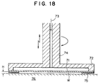
- the apparatus disclosed in the above mentioned Japanese first application entitled "An apparatus for mirror-polishing wafers” uses a flexible elastic membrane 71, by which a wafer is carried on during polishing.
- the membrane 71 are tight-stretched at and along the full periphery with a uniform tension applied by securing the periphery to the lower round end of the wafer mounting head 72.
- a fluid supply source 73 is arranged on the opposite side of the membrane 71 to the wafer W to feed a pressure adjusting fluid on the wafer W.
- the reference numerals 74. 75 and 76 are respectively a rotary shaft, a ring guide plate (or template) adhered to the lower surface of the elastic membrane, and a polishing turn table.
- the elastic membrane 71 which seals the wafer mounting head 72 in the shape of a ring, should be good in flexibility, whereby a uniform distribution of polishing pressure is applied across a wafer W, so that sloping A along the wafer periphery is prevented to occur to the polished wafer.
- the sloping A is illustrated in FIg. 22(b) .
- a polished wafer without the sloping A is shown schematically in section in Fig. 21(b).
- the apparatus for polishing as shown in Fig. 20 comprises a wafer mounting plate 81 made of a rigid material, a mounting pad 82 secured to and across the lower surface of the plate 81, a template 83 in the shape of a ring on the pad 82, a soft polishing pad 85 on the upper surface of a polishing turntable 84, and the polishing turntable 84.
- the front referenced polishing technique claims as indispensable conditions of application the uniform strength distribution of polishing pressure applied to the polished surface of a wafer as shown in Fig. 21(a) (uniformly distributed pressure) and limitation of the pressure application within the back surface area (the surface opposite to the polishing surface) of the wafer W, where the reference numeral 91 in Fig.21(a) designates a wafer mounting plate and the reference numeral 92 indicates a polishing pad.
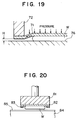
- the elastic membrane 71 is made in uniform thickness and tight-stretched at and along the full periphery in uniform tension to the wafer mounting head 72. Therefore as indicated in Fig.19, in case that the clearance H between the lower surface of the periphery portion of the elastic membrane 71 and the upper surface of the polishing turntable 76 is narrower than a value, the pressure applied in the periphery portion of a wafer grows too big to be normally required as illustrated in Fig.22(a), whereby sloping A comes to be subject to occur along the wafer W periphery.
- the present invention was made. It is an object of the present invention is to provide a method and apparatus to effectively perform the front referenced polishing in which the polished wafer is free from the sloping or raise along the periphery due to poor wafer mounting. It is another object of the present invention to provide a method and apparatus to effectively perform the front referenced polishing in which the surface flatness of the polished wafer is not degraded by inferior machine accuracy by poor assembly, limited accuracy of dimensions in machining of the components, or thermal or mechanical deformation during operation of the apparatus.
- a wafer is secured to a wafer mounting plate in contact with the backside of the wafer and a compressed fluid is supplied to on the side of the upperside of the plate so as to press the wafer toward a polishing turn table, where the influence of the pressure of the compressed fluid is contained within a region of the upperside face of the plate just facing the backside of the wafer mounted.
- the wafer mounting plate may be a thin flexible plate made of a rigid substance on which the wafer mounted, where the region of the flexible plate facing the wafer may be mated with the wafer in a almost perfect geometrical coincidence.
- the region of the wafer mounting plate on which the wafer is mounted which have a flexibility due to the small thickness in spite of being made of a rigid substance is connected to a wafer mounting head along the full periphery of the region of the plate by way of a flexible ring member interposed therebetween and what's more the inner space of the wafer mounting head is communicated with a compressed fluid source.
- the outside region of the wafer mounting plate may be designed to be more flexible than the region facing a wafer mounted, and the outside periphery of the plate may be directly secured to the lower end of the head.
- the thickness across the plate may be changed in such a manner that it is thinner in the outside region than in the region facing the wafer mounted and thereby the flexibility is adjusted so as to be more flexible in the region facing a wafer mounted than in the outside region.
- the thickness is selected in view of a pressure applied in wafer polishing, the elasticity and like that.
- the thickness is preferably between 0.5 mm and 5.0 mm for the region facing a wafer mounted and between 0.3 mm and 3.0 mm for the outside region.
- the thickness is preferred to be between 1.0 mm and 8.0 mm for the region facing a wafer mounted and between 0.5 mm and 4.0 mm for the outsider region.
- the thickness is preferred to be between 0.1 mm and 1.0 mm for the region facing a wafer mounted and between 0.01 mm and 0.05 mm for the outside region
- the thickness is preferred to be between 0.1 mm and 1.0 mm for the region facing a wafer mounted and between 0.01 mm and 0.05 mm for the outside region
- the region facing a wafer mounted may be arranged to have a plurality of vacuum chuck through-holes regularly positioned across the surface and those holes are hermetically sealed on the upperside with soft square rubber codes which have a long groove lengthwise in one of the four side faces, where the groove side is applied onto the upper side of the plate to be disposed to cover the vacuum chuck through-holes and thus a vacuum source may be communicated with all the vacuum chuck through-holes through a single connecting hose, the lower end of which is hermetically secured to a vacuum port of the plate, where the vacuum port is further communicated with all the through-holes by means of the square rubber codes as described above.
- the square rubber codes adhered on to the backside of the plate does not affect the total flexibility of the region.
- the inner space of the wafer holder may be sealed by securing the full periphery of a flexible ring member constructed out of a soft rubber sheet to an inner portion of the head, the inner periphery of which is again adhered to the full periphery of the region of the wafer mounting plate.
- plastic sponge or aggregate of elastic fibres that is, three-dimensionally open cellular structure is applied directly to the perforated surface and further a rubber sheet is used to cover all the plastic sponge or the aggregate of elastic fibres hermetically and still further the underside of the rubber sheet is connected pneumatically to a vacuum source at a vacuum port arranged thereon above the plate centre portion.
- a soft rubber plate a lower side of which a spiral groove is formed across, may be superimposed on the wafer mounting plate so that the spiral groove is positioned to communicate with all the vacuum through-holes in full and further the spiral groove of the soft rubber plate is hermetically connected to a vacuum source by way of a flexible hose.
- the present invention is always described with an emphasis on a method and apparatus for polishing a wafer at a time. however, a plurality of the structures similar to the wafer mounting plate with a wafer mounted thereunder and the components acompanied may be contained in the same opening of a larger wafer mounting head.
- a wafer is mounted on the lower side of the wafer mounting plate, a compressed fluid, for example, air is supplied to the space above the wafer from a compressed fluid source, and the wafer is pushed onto a polishing turntable at a pressure by the displacement of the plate by increase in the pressure of the space, so that the wafer polishing is operated on in the usual manner of the prior art.
- a compressed fluid for example, air is supplied to the space above the wafer from a compressed fluid source, and the wafer is pushed onto a polishing turntable at a pressure by the displacement of the plate by increase in the pressure of the space, so that the wafer polishing is operated on in the usual manner of the prior art.
- the flexible ring member is expandable or shrinkable to follow the displacement of the plate according to the pressure of the fluid in the space.
- the plate is constructed out of a thin plate of hard rubber and the like in the region facing a wafer mounted, so that the wafer is applied across the whole backside with uniform polishing pressure and that with application of the pressure strictly limited within the backside of the wafer as well as with flexible local deformation of the plate exactly following the surface contour of the backside of the wafer.
- global deformation of the wafer for example, bow is straighten on a polishing pad under polishing pressure.
- the inner periphery of the flexible ring member is secured to the periphery region of a wafer mounting plate facing a wafer mounted and the region facing the wafer is only applied with the pressure, so that the ring member works as a moving region together with the outside region and thereby errors in the machine assembly, poor dimensional accuracy of the components, or the thermal or mechanical deformation built-up with time elapsed in operation, which otherwise unavoidably amount to values on the order of ⁇ ms to tens of ⁇ ms in an extreme case, is never inactive on the flatness even of close tolerances of the polished wafer surface required in VLSI technology.
- the apparatus in which a wafer mounting plate directly secures the backside of a wafer on the lower side and a compressed fluid is supplied on to the upper side and the wafer is polished in contact under pressure with a polishing pad, comprises a wafer mounting head with a cylindrical body open downward and an annular downward projection integral therewith on the ceiling, a wafer mounting plate concentrically secured on the lower end of a short hollow cylinder and arranged by a template for surrounding and receiving a wafer on and along the full periphery of the lower surface of the plate, a sealed space produced by hermetically connecting an expansion pipe both with the annualar downward projection and with the plate respectively, a highly flexible support for supporting the plate in place secured both on and along the inner periphery of the cylindrical body open downward and along the outer periphery of the short hollow cylinder, and a flexible hose hermetically connected both with a vacuum port in the center portion of the ceiling and a vacuum port in the center portion
- the plate may be structured out of a rigid thin plate with a less flexibility than that of the flexible supporter surrounding the plate inside the cylindrical body of the head, where the flexible supporter serves the only one moving region within the head.
- the sealed space in the head is designed to be in the rough duplicates in shape and dimension of section both on the side of the plate and on the side of the head.
- the rigid thin plate for making of the wafer plate mounting plate for example, thin plates made of hard plastics, hard rubber, metal and so on may be listed.
- the hard plastics comprises such thermosetting resins as epoxy resin, phenol resin and such heat resistant hard resins as polyethylene terephtalate, polybuthylene telephtalate, polyimide, polysulfone and so on and they may be reinforced by glass fibres, carbon fibers, woven or nonwoven stuff thereof or the like.
- the hard plastics and hard rubber, inculding the substances with reinforcement by the above mentioned fibres or the fabrics thereof preferably have a thickness in the range of between 0.1 mm and 1.0 mm so as to show their flexibility in the form of a plate.
- the thicknesses according to the second aspect of the present invention are in general thinner than those of the first aspect of the present invention due to the structural differences therebetween around the wafer mounting plate.
- the thickness of the plate may be chosen in the range between 0.05 mm 0.2 mm to secure the flexibility in the form of a plate.
- the wafer carrier is suspended in the inner space of the wafer mounting head by the expansion pipe and the flexible supporter respectively secured to the different portions of the head, so that in a way similar to or more effective than the apparatus according to the first aspect of the present invention, errors is the machine assembly, poor dimensional accuracy of the components, or the thermal or mechanical deformation accumulated in the structure with time past in operation, which unavoidably amounts to a level on the order of ⁇ ms or tens of ⁇ ms in the worst, do not any more affect the flatness of a polished wafer to close tolerances and what's more the wafer is pressed on in a stable and assured way onto the polishing pad during operation.
- the mounted wafer is directly held on the lower side of the flexible plate and the flexible plate is pressed from the upper side by the compressed air.
- the bow of the wafer is thereby corrected and the plate itself is deformable following the local variation of the wafer thickness while still keeping the direct contactness all over the wafer back surface, so that the polishing surface of the wafer may be brought into a close contact as a whole with the polishing pad without any transmission of projections or recesses on the back surface to the front surface.
- the plate is permitted to be geometrically adaptable even in a microscopic sense to the surface contour of the wafer backside due to the cushioning effect of resilience.
- the wafer carrier comprises the short hollow cylinder that is rigid which supports the periphery of the plate and the plate which consists of the region facing a wafer mounted and the periphery region more flexible than the former' and forming a moving region. Accordingly, the flexible supporter does not deform the central region since the deformation resulted in the shape of the flexible supporter can not propagate across the moving region toward the center region of the plate, where the deformation of the flexible supporter is caused by the tensions generated within the supporter during the polishing.
- the vertical component of the tension of the flexible supporter and the self weigh of the short hollow cylinder, combined, are received by the template which is arranged beneath the plate periphery portion and which cages to retain a wafer within and the force pressing down the center region may be the one from a compressed air only and thereby the pressure acting the polishing front face may be controlled uniform across the whole face.
- the force acting from the side of the mounting head is larger than that, based on the pressure of the compressed air , pushing the wafer to the polishing pad from the wafer back side due to uniformity of the air pressure within the sealed space, so that the difference in magnitude between the forces is transmitted to the template by way of the short hollow cylinder and at the same time from the wafer mounting plate to the wafer.
- the force acting on the wafer consists of the only one, which is the air pressure, and thereby the polishing pressure may be uniform across the polishing face.
- the polishing pressure across the polishing face comes to be uniformly applied all over and thereby stock removal rates are constant at any point across the face, so that the front referenced planarization polishing may become a reality in practical use.
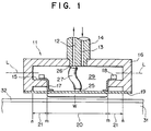
- Fig. 1 is a sectional view of the principal part of an apparatus for polishing a semiconductor wafer, where only one wafer is polished at a time.
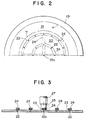
- Fig. 2 is a plan view of the wafer mounting plate ( hereinafter referred to as a mounting plate.)
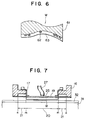
- Fig. 3 is the sectional view of the mounting plate.
- the mounting plate works as a vacuum chuck plate having a plurality of vacuum chuck holes therein and as shown in Fig, 1.
- the wafer holder 11, which carries and turns a wafer thereon, is facing the polishing pad 31 and adapted to be shiftable both upward and downward.
- the wafer mounting head 16 and mounting plate 19 are the principal parts of structure of an apparatus according to the first aspect of the present invention.
- the wafer holder 11 comprises the rotary shaft 14, through which the passes 12 and 13 are formed, the wafer mounting head 16 that is hollow and cylindrical, which is secured to the lower end of the rotary shaft 14, the ring projection 15 that is horizontally and inwardly extending, which is secured integrally to the inner periphery wall of the wafer mounting head 16 and the wafer mounting plate 19.
- the rotary shaft 14 is adapted to be rotatable and shiftable vertically by an external drive.
- the passes 12 and 13 are communicated with a vacuum pump and a compressor (neither of them shown) respectively.
- the ring projection 15 of the wafer holder 16 works as the place on which the upper flange of a flexible ring member 17 being constructed of a pan-shaped highly elastic sheet, for example a rubber sheet (hereinafter a flexible ring member will be also called a pan-shaped highly elastic sheet or a rubber sheet as well with the same reference numeral 17), is secured with screws and an annular mounting member 18 superimposed on the upper flange of the pan-shaped sheet 17, where the pan-shaped sheet 17 has a downward round opening in the centre portion, and effectively seals the annular securing portion on the upper face of the ring projection 15 with the elasticity of its own.
- the downward round opening of the sheet 17 has the same diameter as that of a wafer to be polished.
- the wafer mounting plate 19 is constructed out of a round thin disk made of such hard substances as hard plastics, hard rubber, metal and the like and thereby is designed to have an flexibility.
- the wafer mounting plate 19 comprises a round wafer holding region (a portion facing a wafer mounted) 20 in the center portion and the outside annular region 21, which is designed to be more flexible than the wafer holding region 20, which constitutes a moving region.
- the difference in flexibility between the wafer holding region 20 and the moving region 21 is realized by ,for example, making the thickness of the moving region 21 thinner or perforating a plurality of through-holes in the outside annular region 21 as will be described later in more detail.
- the mark m in Figs, 1 and 2 indicates the boundary between the wafer holding region 20 and the moving region 21 and the mark n indicates the boundary between the moving region 21 and the inner periphery of the lower end of the mounting head 16, where the mounting plate 19 is also secured onto the lower end.
- the holding region 20 of the mounting plate 19 has a plurality of vacuum chuck holes 22 (hereinafter referred to as a chuck hole) perforated through as shown in Fig 2.
- the chuck holes 22 consist of one in the center portion of the holding plate and the others arranged on a plurality of concentric circles around the center.
- the thin, narrow soft rubber codes 24 (or soft plastic codes) with a long groove 23 on one of the four sides are adhered onto the upperside surface of the mounting plate 19, which is the surface opposite to the surface where a wafer is mounted and thereby, seal all the chuck holes 22 including a vacuum hole 22c in the center portion to get each of the chuck holes 22 to hermetically communicate with all the other holes 22.
- the hollow connector 25 (see Fig.1 and 3) is mounted as a vacuum port at the chuck hole 22c in the center portion.
- another hollow connector 26 as a vacuum port is mounted at the opening end of the pass 12 formed through the rotary shaft 14 and the flexible hose 27 constructed out of a rubber hose is arranged between the connecters 25 and 26 for a hermetic communication.
- the outer periphery of the holding plate 19 is secured with screws along the lower end of the wafer mounting head 16.
- the wafer holding region 20 of the holding plate 19 is adhered along the full outer periphery to the annular lower end of the rubber sheet 17 to generate a sealed space 29 within the wafer holder 11.
- the structure as shown in Fig. 1 of the wafer holder 11 may be preferably divided into the two portion of the upper and the lower halves in order to be easy to overhaul or assemble.
- the structure is designed so as to be dismantled into the two portions being in a fitting relation at a horizontal intersecting plane on the alternate long and short dash line L-L in Fig.1 and to be set up with suitable fixturing means such as bolts and nuts in assembly.
- an easy and quick assembly may be realized in the steps of securing the mounting plate 19 onto the lower half of the wafer mounting head 16, connecting the flexible hose 27 with the vacuum ports 25 and 26, finally combining and fixturing the two halves into one.
- the mounting plate 19 comprises the wafer holding region 20 and the moving region 21 which is higher in flexibility than the wafer holding region(the examples will be explained later.) and the full periphery of the holding region 20 is secured on the rubber sheet 17 and besides the periphery of the mounting plate 19 is secured to fix on the lower end of the wafer mounting head 16.
- a plastic sheet in the shape of bellows may be used instead of the rubber sheet 17 as a pan-shaped sheet.
- Substance and a structure of the pan-shaped sheet have a limitation on the nature that the sheet may be freely shrinkable or extendible in accordance with the fluid pressure inside the wafer holder 11.
- Substances for constructing the mounting plate 19 are required to have such properties as a mechanical strength, flexibility, elasticity and heat resistance in suitable respective levels.
- the preferable among plastics are, for example, thermosetting resin, heat resistant thermoplastic resin, reinforced resins thereof mixed with glass fiber or plastic fiber, or laminated sheet thereof reinforced with fibres or paper.
- a thin plate made or constructed out of hard rubber or thin metallic sheet with anticorrosiveness may be used as substitute for plastic plate.
- the polishing pad 32 mounted on the polishing turntable 31 should not be subject to plastic deformation and may preferably be selected from a group comprising polishing pads constructed out of close cell type of polyurethane foam, polyurethane impregnated polyester non woven fabric and the like, which are well known in the prior art.
- the vacuum pump is actuated to breathe out the atmosphere in the holes in the mounting plate 19 and gap between the mounting plate 19 and the wafer W through the pass 12, whereby the wafer, as shown in section in Fig. 4 (where for better understanding the global surface undulation and minute step projections are shown in exaggeration.), is vacuum chucked on the mounting plate 19.
- the compressor gets started to feed a compressed air controlled at a given pressure to the sealed space 29 and thereby the mounting plate 19 and the rubber sheet 17 are displaced in a mutual positional relation kept unchanged with each other to force the wafer to be pressed onto the polishing pad 32 and in due course to get the wafer being polished under the well known mechanism.
- the rubber codes 24 are used to have the vacuum holes 22 in the plate 19 to be communicated with each other, so that the loss in flexibility is not brought about to the wafer holding region 20 of the mounting plate 19 and in addition to that, the flexible hose 27 is adopted as a member to communicate the mounting plate 19 with the pass 12 for evacuation and as a result the mounting plate 19 is free to displace the position in accordance with the pressure of the compressed air fed by way of the pass 13.
- the wafer mounting plate 19 is secured the lower end of the wafer mounting head 16, whereby the wafer may keep a constant position against the frictional force acting to the polishing surface of the wafer.
- the oxide film 63 covering the wafer front face is, as shown in Fig. 5, kept in a stable close contact with the polishing pad 32 all over the surface and in due course is polished in such a manner that the mounting plate 19 is kept under uniformity of polishing pressure across all the upperface and that in a condition in which the region thus under the influence of the polishing pressure is strictly confined within the back face space of the wafer W and in addition the mounting plate 19 is deformed to copy the wafer back surface in the surface morphology adapted in detail thereto.
- a minute step projections on the oxide film 64 which correspond to interconnections 62 deposited on the preceding surface, with the one to one basis, is selectively polished faster with less stock removal on the other area and that without periphery slopings due to more local removal rates or high spots generated due to less local removal rates around the wafer periphery region, whereby the thickness of the oxide 63 remains flat and parallel to the preceding surface during the polishing according to the above embodiment of the present invention.
- the apparatus for polishing have a wafer mounting plate 19, which is spatially divided into a moving region 21 higher in flexibility than a wafer holding region 20 and the wafer holding region 20.
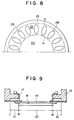
- the mounting plate 19 is constructed out of the same and one substance and as shown in Fig. 7, the moving region 21 smaller in thickness than the holding region 20.
- the preferred range of the thickness of the mounting plate 19 is affected by the polishing pressure of a wafer, the elasticity of the substance constructing the mounting plate.
- the thickness may be preferably selected in the range of 0.5 mm ⁇ 5.0 mm for the holding region 20 and in the range of 0.3 mm ⁇ 3.0 mm for the moving region 21, as for a hard rubber thin plate, in the range of 1.0 mm ⁇ 8.0 mm for the holding region 20 and in the range of 0.5 mm ⁇ 4.0 mm for the moving region 21, and as for a metal thin plate, in the range of 0.1 mm ⁇ 1.0 mm for the holding region 20 and in the range of 0.01 mm ⁇ 0.05 mm for the moving region 21.
- an apparatus according to the first aspect in general adopts a thicker plate with respect to both the wafer holding region 20 and moving region 21, since the first aspect lacks in the rigid short hollow cylinder of the second aspect surrounding the mounting plate 19 and being kept strictly in a body therewith when moving.
- the wafer mounting plate 19 is constructed as shown in Fig. 8 out of the same and one substance and a thin plate having a uniform thickness across it and includes a moving region 21 with a plurally of through-holes 28 in the shape of eclipse, circle or segment, where instead of through-holes 28 a plurally of recesses in the same shapes may be adopted with the thin recess bottom thereof, and that with a plurally of the recesses dispersed almost all over the moving region 21, eventually making the average thickness of the region to be thinner.
- the mounting plate 19 is constructed as shown in Fig.9 out of a two different substances, one of which is of hard plastic for the holding region 20 and the other of which is of rubber sheet mixed with plastic fibers, plastic fabrics or knitted sheet for the moving region 21.
- the two regions are connected with each other along the full peripheries.
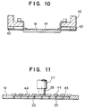
- the wafer mounting plate 19 is secured on the wafer mounting head 16 with a annular soft rubber sheet 42 interposed therebetween as shown in Fig.10. Examples of vacuum-related structures of the wafer mounting plate 19 are illustrated in the following description.
- a plurality of vacuum chuck holes 22 are arranged on the side mounting a wafer of the wafer mounting plate 19.
- the chuck holes have a depth reaching the mid point of the thickness and are arranged to locate with one at the centre and the others on concentric circles around the centre.
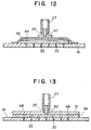
- Spiral groove 43 half way in depth is formed in the upperside surface of the mounting plate 19 to communicate with vacuum chuck holes 22.
- the spiral groove 43 is sealed with a spirally arranged code member 44, which is made of soft rubber or soft plastics.
- a vacuum port 25 is disposed at the centre portion, where the centre of the spiral groove 43 is also located. The vacuum port 25 is connected the flexible hose.
- vacuum chuck holes 22 of the mounting plate 19 are formed as through-holes in the bulk and covered with plastic sponge 45 (or aggregate of elastic fibers) on the upperside of the mounting plate 19.
- the sponge 45 is again covered with a soft rubber cover 46 at the center portion of which a through-hole 47 is opened.
- the through-hole 47 is communicated with a vacuum source by way of a vacuum port 25 and thereafter a flexible hose 27 disposed in that order.
- the vacuum chuck holes 22 are formed as a through hole in the bulk of the mounting plate 19.
- a soft rubber made plate member 49 in which a spiral bottomless groove 48 is formed, is superimposed on the upperside of the mounting plate 19 in such a manner that the vacuum holes are all communicated with the spiral bottomless groove 48.
- a soft rubber cover 51 which have a through-hole 50 in the central portion, is placed on the plate member 49 to cover.
- the through-hole 50 is adjusted laterally to communicate with a part of the spiral bottomless groove 48 and furthermore is communicated with a vacuum source by way of a vacuum port 25 and a flexible hose 27.
- a wafer mounting plate 19 has a spiral groove 43 on the front side and a through-hole 52 in the center portion.
- the spiral groove 43 and the through-hole 52 are communicatable with each other.
- the through-hole 52 is further communicated with a vacuum source by way of a vacuum port 25 and a flexible hose 27.
- a wafer mounting plate 19 has a plurality of through-holes 22 formed therein.
- a soft rubber made cover 53 has a spiral groove 43 on the lower side and a through-hole 52 at the centre of the spiral groove 43, where the groove and the through-hole 52 are communicated with each other. And the cover 53 is superimposed with lateral adjustment on the upperside of the mounting plate 19 to communicate with the spiral groove 43 and in addition to that, the through-hole 52 is made to communicate with a vacuum source by way of a vacuum port 25 and a flexible hose arranged in that order.
- vacuum holes 22 are formed as a through-hole in the mounting plate 19, further is communicated with a manifold 54 made of soft rubber or soft resin, where a manifold also communicated with a vacuum source by way of a flexible hose (not shown).
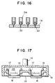
- Fig. 17 comprises a plurality of annular mounting members 18 and pan-shaped rubber sheets 17 secured to a wafer mounting head 16 and a plurality of wafer mounting plates 19 are also connected with the lower end of the wafer mounting head 16, which is equipped with a plurality of downward openings.
- the mounting plates 19 holds a plurality of wafers, each on each, to polish during the same and one operation, where a larger sealed space 29 is formed for common use within the wafer mounting head 16.
- all the mounting plates 19 are of a type of vacuum chucking but another type of mounting may be allowed to be in use for a method of polishing semiconductor wafers and apparatus therefor still within the spirit and scope of the present invention, in which the backside of a wafer is pressed to attach to a wetted resilient film having a microscopic open pore structure in the surface (hereafter referred to as backing pad fixturing).
- backing pad fixturing the attractive force between the film and wafer is too weak to resist shear forces during polishing and therefore the wafer edge have to caged by a retaining ring or a template secured on the lower face periphery of the wafer mounting plate 19.
- Fig. 24 is a sectional view showing an example embodying the principal part of a polishing apparatus according to the second aspect of the present invention.
- Fig. 25 is a plan view of a wafer mounting plate 102 of the example.
- Fig. 26 is a sectional view of the wafer mounting plate 102 shown in Fig. 25.
- a wafer holder 111 in which a wafer is held to rotate with which, is disposed above a polishing turn table 31 and is shiftable either upward or downward.
- the wafer holder 111 comprises a rotary shaft 14 in which passes 12 and 13 are formed, a wafer mounting head 106, which is fixedly secured to the lower end of the rotary shaft 14, a cylindrical hollow body open downward 106a and an annular downward projection 106b around the center of the ceiling of the inner space, which are both constituted integrally as parts of the wafer mounting head 106, and a wafer carrier 104 including a wafer mounting plate 102.
- the wafer carrier 104 which structure is detailed below, is secured to the wafer mounting head 106.
- the wafer carrier 104 is composed of the wafer mounting plate 102 (hereinafter referred to as a mounting plate.) and an annular template 103 secured on the lower face of the mounting plate 102.
- a short hollow cylinder 101 which is a component of the wafer carrier 104, is connected to the annular downward projection 106b on the inner periphery wall at least for sealing to eventually form a sealing space 107.
- the short hollow cylinder 101 is, on the other hand, connected to near the lower end of the cylindrical hollow body 106a by means of a interposing flexible support 108, which may be constructed out of, a plurality of high flexibility metal thin wires arrayed in all the radial directions from and around the short hollow cylinder 101 and combined into the form of an annular sheet, or as alternates an annular rubber, plastic, metallic or the like thin plate.
- the wafer carrier 104 is three-dimensionally free to shift a position due to the special structure of being suspended in the air inside the wafer mounting head 106.
- the pass 12 is communicated with a vacuum pump(not shown) by way of a pipe and valve (both not shown) and as shown in Figs. 25 and 26, vacuum chuck hole 22 (hereinafter referred to a chuck hole) in the mounting plate 102 are communicated with the fluid pass 12 by a vacuum port 25 disposed in the center portion of the mounting plate 102, a flexible hose 27 and a vacuum port 26 disposed in the center portion of the ceiling of the sealed space 107.
- the pass 12 is connected to a compressor (not shown ) by way of a pipe and a valve (both not shown) and further makes it possible to feed a compressed air into the sealed space 107.
- a plurality of chuck holes 22 as a through-hole formed in the mounting plate 102 are consisting of one in the central portion of the mounting plate 102 and the others on and along concentric circles about the one in the central portion.
- Soft rubber cords 24 (or soft rubber belts, which are small in both width and thickness, which have a long groove longitudinally on one of the sides, are adhered on the upperside of the mounting plate 102, that is, on the face opposite to the face on which a wafer is chucked, not only to seal all the chucked holes but also to make the chuck hole 22c in the central portion to communicate with all the other holes 22.
- the vacuum port 25 is disposed at the chuck hole 22c in the central portion of the mounting plate 102.
- the vacuum port 26 is disposed at the open end of the pass 12.
- the flexible hose 27 such as a rubber hose and the like is connected between the vacuum ports 25 and 26.
- the mounting plate 102 is all constructed out of a hard plastic plate, a hard rubber plate, a metallic plate or the like with a proper flexibility as a physical property. Different flexibilities may be preferably adopted for the respective two regions consisting of a less flexible wafer holding region 102a, on which the backside face of a wafer kept in contact, and a more flexible moving region 102b, which is annular in shape and which is the portion other than the wafer holding region (as shown in Figs. 24 ⁇ 26). The two regions are both under the influence of a compressed air at the same time.
- the mark m in Figs. 24 ⁇ 26 designates a boundary on which the mounting plate 102 is divided into the wafer holding region 102a and the moving region 102b and the mark n indicates a boundary between the moving region 102b and a fixture portion in the short hollow cylinder 101.
- the poorer uniformity is invited to the strength distribution profile of the force applied over the wafer with an increase in the width of the moving region 102b and therefore the better performance with the above structure is resulted in, the narrower in the width and/or the higher in the flexibility the moving region 102b is.
- thermosetting plastics or heat resistant thermoplastic resin with a moduli of elasticity either for tensile stress or for bending stress of both more than 5000 kf/cm2 and a thickness in the range of 0.1 mm ⁇ 1.0 mm.
- the hard rubber thin plate selected is the one having a thickness in the range of 0.1 mm ⁇ 8 mm and being made of ebonite or the like substances with a hardness equal to that of ebonite.
- stainless steel is selected as a substance and the thickness between 0.05 mm and 0.20 mm.
- the moving region 102b may be preferably designed to keep as narrow in the width as possible.
- the thicker wafer holding region 102a for example, may be chosen to increase a relative flexibility of the moving region 102b over that of the wafer holding region 102a. It is very easy to adjust the flexibility differential between the regions by use of the effect from thickness differential.
- the expansion pipe 105 is constructed out of, for example, a soft rubber sheet or the one reinforced by plastic fibres.
- the highly flexible support 108 may be constructed out of radially arranged thin metallic wires or a thin plate of rubber, plastic or metal.
- the sealed space 107 preferably coincides with a wafer mounted in cross sectional shape and dimensions both on the side of the wafer carrier 104 and on the side of the wafer mounting head 106.
- a wafer W shown in section in Fig. 4 is vacuum chucked on the wafer mounting plate 102 by a vacuum pump actuated.
- a wafer W may be chucked on the lower surface of the mounting plate 102 leaving a proper gap between the wafer and the inner periphery of the template 103.
- the chucking position is not specialized on the mounting plate, but if the mounting plate 102 is constructed out of the two of the holding region 102a and more flexible moving region 102b, the periphery of the wafer W have to be positioned so as to be precisely coincided with the periphery of the holding region 102a.
- Compressed air controlled at a pressure is supplied into the sealed space 107 to press the upperside of the mounting plate 102 and further to shift the wafer carrier 104 presses the wafer W onto a polishing pad 32 on a polishing turn table 31, so that thereafter on the wafer is polished under the same conditions as applied in the prior art.
- the wafer carrier 104 is suspended from the wafer mounting head 106 by the expandable and highly flexible members 105 and 108, the rubber cords 24 are used to have the chuck holes 22 of the mounting plate 102 to communicate with each other, such that any loss in the flexibility of the mounting plate 102 is not materialized.
- the load applied on the wafer carrier 104 is designed to be received by the template 103 arranged on a part of the lower end face of the mounting plate 102.
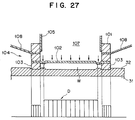
- the wafer holding region 102a is made flexible, and the flexible hose 27 is equipped to communicate the vacuum chuck holes 22 with the vacuum pass 12, So that the wafer mounting table 102 is, as shown in Fig. 27, freely displaced in accordance with the pressure of the compressed air as well as is deformable in conformity with the surface contour of the wafer W backside, the entire oxide film 63 on the front face of the wafer is, as shown in Fig. 5, put in close contact with the surface of the polishing pad 32 and the polishing pressure distribution profile D across all the backside face of the wafer comes to be uniform.
- Such projections as minute steps or high spots of the oxide film 64 are selectively polished off without producing sloping at the periphery due to local excess polishing or projections at or around the periphery due to, to the contrary, local poor polishing and thereby the oxide film 63 is polished off under conditions where removal rates are globally uniform all over the surface.
- the polished wafer W as shown in Fig. 6, may be obtained with the oxide film 63 of uniform thickness across the surface.
- the wafer mounting plate 102 is constructed out of the wafer holding region 102a lower and the moving region 102b higher in the flexibility and besides the periphery of the wafer W is positioned to coincide with the periphery of the wafer holding region 102a, so that the pressure in the vicinity of the wafer periphery may be control at the same strength as the rest portion with more ease than a case when all the mounting plate 102 is constructed out of a homogeneous flexible hard plastic and the like. Consequently the overall thickness of the oxide film 63 may be easier to obtain uniform as well as the flatness may be achieved of close tolerances across the wafer surface required for better performance of optical lithography in the making of a semiconductor electronics device.
- a wafer mounting plate 102 As is the same for the first aspect of the present invention, a wafer mounting plate 102 may be replaced by another wafer mounting plate on which the backing pad fixture is adopted as explained in the first aspect of the present invention.
- a method of polishing semiconductor wafers and apparatus therefor is featuring that in the apparatus, a pressure applying region is spatially restricted within the front polishing face of a wafer mounted, and a wafer holding region is flexible and constructed out of a hard plastic plate, so that the polishing pressure is applied in uniform distribution profile all over the wafer and restricted not to give any influence thereof outside of the backside face of the wafer and thereby the wafer is polished with the wafer mounting plate flexibly deformed in conformity with the global surface contour of the backside of the wafer.
- the so-called planarization to be applied in the fabrication process of a semiconductor device is effectively realized in practical sense and thereby an oxide film or an interlevel dielectric film having both a uniform thickness and a flatness to close tolerances across a wafer or substrate may be obtained without any minute high spot left unpolished off.
- the planarization technique thus achieved may make the processing yield in multilevel interconnections of VLSI technology improved as well as the reliability of a semiconductor device product higher.
- the wafer mounting plate is supported indirectly by the flexible support with the short hollow cylinder lying therebetween, which interfere with transmission of the stress caused by deformation in the flexible support to the wafer mounting plate, is free to be displaced three-dimensionally in a body with the other parts of the wafer carrier and besides is flexibly deformed to conform with the global surface contour of the backside of the wafer mounted under uniform strength distribution profile of polishing pressure across the entire wafer during a polishing operation, so that a polished wafer may be produced without slopings due to over polishing or high spots due to underpolishing along or in the vicinity of the periphery and thereby according to the second aspect, a front referenced polishing of a higher performance may be guaranteed to achieve.
Landscapes
- Engineering & Computer Science (AREA)
- Mechanical Engineering (AREA)
- Finish Polishing, Edge Sharpening, And Grinding By Specific Grinding Devices (AREA)
- Mechanical Treatment Of Semiconductor (AREA)
Applications Claiming Priority (6)
| Application Number | Priority Date | Filing Date | Title |
|---|---|---|---|
| JP28439393 | 1993-10-18 | ||
| JP28439393A JP2891068B2 (ja) | 1993-10-18 | 1993-10-18 | ウエーハの研磨方法および研磨装置 |
| JP284393/93 | 1993-10-18 | ||
| JP291330/93 | 1993-10-27 | ||
| JP29133093 | 1993-10-27 | ||
| JP29133093A JP2757112B2 (ja) | 1993-10-27 | 1993-10-27 | ウエーハ研磨装置 |
Publications (2)
| Publication Number | Publication Date |
|---|---|
| EP0653270A1 true EP0653270A1 (fr) | 1995-05-17 |
| EP0653270B1 EP0653270B1 (fr) | 1999-07-14 |
Family
ID=26555451
Family Applications (1)
| Application Number | Title | Priority Date | Filing Date |
|---|---|---|---|
| EP94306406A Expired - Lifetime EP0653270B1 (fr) | 1993-10-18 | 1994-08-31 | Méthode de polissage de wafers semi-conducteurs et appareil pour son exécution |
Country Status (3)
| Country | Link |
|---|---|
| US (1) | US5584746A (fr) |
| EP (1) | EP0653270B1 (fr) |
| DE (1) | DE69419479T2 (fr) |
Cited By (27)
| Publication number | Priority date | Publication date | Assignee | Title |
|---|---|---|---|---|
| WO1997000155A1 (fr) * | 1995-06-16 | 1997-01-03 | Optical Generics Limited | Procede de polissage optique et appareil associe |
| EP0747167A3 (fr) * | 1995-06-09 | 1997-01-29 | Applied Materials Inc | Appareil pour retenir une plaquette pendant le polissage |
| GB2317131A (en) * | 1995-06-16 | 1998-03-18 | Optical Generics Ltd | Method and apparatus for optical polishing |
| EP0841123A1 (fr) * | 1996-11-08 | 1998-05-13 | Applied Materials, Inc. | Plaque de support avec membrane flexible pour un dispositif de polissage mécano-chimique |
| EP0879678A1 (fr) * | 1997-05-23 | 1998-11-25 | Applied Materials, Inc. | Plaque de support avec dispositif de détection de substrat pour un dispositif de polissage mécano-chimique |
| EP0859399A3 (fr) * | 1997-02-13 | 1999-03-24 | Integrated Process Equipment Corp. | Appareil de polissage de tranche de semiconducteur avec plaque de support flexible |
| EP0922531A1 (fr) * | 1997-12-11 | 1999-06-16 | Speedfam Co., Ltd. | Support et dispositif de polissage mécano-chimique |
| US5964653A (en) * | 1997-07-11 | 1999-10-12 | Applied Materials, Inc. | Carrier head with a flexible membrane for a chemical mechanical polishing system |
| US5993302A (en) * | 1997-12-31 | 1999-11-30 | Applied Materials, Inc. | Carrier head with a removable retaining ring for a chemical mechanical polishing apparatus |
| US6080050A (en) * | 1997-12-31 | 2000-06-27 | Applied Materials, Inc. | Carrier head including a flexible membrane and a compliant backing member for a chemical mechanical polishing apparatus |
| US6146259A (en) * | 1996-11-08 | 2000-11-14 | Applied Materials, Inc. | Carrier head with local pressure control for a chemical mechanical polishing apparatus |
| GB2315365B (en) * | 1996-07-12 | 2001-05-30 | Tokyo Seimitsu Co Ltd | Semiconductor wafer polishing machine |
| EP1125686A4 (fr) * | 1999-02-12 | 2002-04-24 | Shinetsu Handotai Kk | Disque de maintien de piece pour polissage, appareil de maintien de piece et procede de polissage de piece |
| US6386947B2 (en) | 2000-02-29 | 2002-05-14 | Applied Materials, Inc. | Method and apparatus for detecting wafer slipouts |
| EP1031398A3 (fr) * | 1999-02-25 | 2002-05-22 | Obsidian, Inc. | Stabilisateur d'un moyen de polissage |
| US6398621B1 (en) | 1997-05-23 | 2002-06-04 | Applied Materials, Inc. | Carrier head with a substrate sensor |
| EP0947288A3 (fr) * | 1998-04-02 | 2002-06-05 | SpeedFam-IPEC Inc. | Support et dispositif de polissage mécano-chimique |
| US6485359B1 (en) | 2000-09-15 | 2002-11-26 | Applied Materials, Inc. | Platen arrangement for a chemical-mechanical planarization apparatus |
| EP1029632A3 (fr) * | 1999-02-17 | 2002-12-04 | Fujikoshi Kikai Kogyo Kabushiki Kaisha | Machine d'usinage par abrasion |
| US6561884B1 (en) | 2000-08-29 | 2003-05-13 | Applied Materials, Inc. | Web lift system for chemical mechanical planarization |
| US6722965B2 (en) | 2000-07-11 | 2004-04-20 | Applied Materials Inc. | Carrier head with flexible membranes to provide controllable pressure and loading area |
| US6837964B2 (en) | 2001-08-16 | 2005-01-04 | Applied Materials, Inc. | Integrated platen assembly for a chemical mechanical planarization system |
| US6857945B1 (en) | 2000-07-25 | 2005-02-22 | Applied Materials, Inc. | Multi-chamber carrier head with a flexible membrane |
| US6872122B2 (en) | 1998-12-30 | 2005-03-29 | Applied Materials, Inc. | Apparatus and method of detecting a substrate in a carrier head |
| US7198561B2 (en) | 2000-07-25 | 2007-04-03 | Applied Materials, Inc. | Flexible membrane for multi-chamber carrier head |
| US7255771B2 (en) | 2004-03-26 | 2007-08-14 | Applied Materials, Inc. | Multiple zone carrier head with flexible membrane |
| WO2009146274A1 (fr) * | 2008-05-30 | 2009-12-03 | Memc Electronic Materials, Inc. | Appareil de polissage de tranche de semi-conducteur et procédé de polissage |
Families Citing this family (84)
| Publication number | Priority date | Publication date | Assignee | Title |
|---|---|---|---|---|
| US5643053A (en) | 1993-12-27 | 1997-07-01 | Applied Materials, Inc. | Chemical mechanical polishing apparatus with improved polishing control |
| US5908530A (en) * | 1995-05-18 | 1999-06-01 | Obsidian, Inc. | Apparatus for chemical mechanical polishing |
| JPH09225819A (ja) * | 1996-02-21 | 1997-09-02 | Shin Etsu Handotai Co Ltd | 被加工物の保持機構 |
| US5876273A (en) * | 1996-04-01 | 1999-03-02 | Kabushiki Kaisha Toshiba | Apparatus for polishing a wafer |
| US6036587A (en) * | 1996-10-10 | 2000-03-14 | Applied Materials, Inc. | Carrier head with layer of conformable material for a chemical mechanical polishing system |
| US5830806A (en) * | 1996-10-18 | 1998-11-03 | Micron Technology, Inc. | Wafer backing member for mechanical and chemical-mechanical planarization of substrates |
| US5941758A (en) * | 1996-11-13 | 1999-08-24 | Intel Corporation | Method and apparatus for chemical-mechanical polishing |
| DE19651761A1 (de) * | 1996-12-12 | 1998-06-18 | Wacker Siltronic Halbleitermat | Verfahren und Vorrichtung zum Polieren von Halbleiterscheiben |
| US6056632A (en) * | 1997-02-13 | 2000-05-02 | Speedfam-Ipec Corp. | Semiconductor wafer polishing apparatus with a variable polishing force wafer carrier head |
| US5993298A (en) * | 1997-03-06 | 1999-11-30 | Keltech Engineering | Lapping apparatus and process with controlled liquid flow across the lapping surface |
| US5910041A (en) * | 1997-03-06 | 1999-06-08 | Keltech Engineering | Lapping apparatus and process with raised edge on platen |
| US5967882A (en) * | 1997-03-06 | 1999-10-19 | Keltech Engineering | Lapping apparatus and process with two opposed lapping platens |
| US6048254A (en) * | 1997-03-06 | 2000-04-11 | Keltech Engineering | Lapping apparatus and process with annular abrasive area |
| US6149506A (en) * | 1998-10-07 | 2000-11-21 | Keltech Engineering | Lapping apparatus and method for high speed lapping with a rotatable abrasive platen |
| US6120352A (en) * | 1997-03-06 | 2000-09-19 | Keltech Engineering | Lapping apparatus and lapping method using abrasive sheets |
| US6203414B1 (en) * | 1997-04-04 | 2001-03-20 | Tokyo Seimitsu Co., Ltd. | Polishing apparatus |
| US6244946B1 (en) | 1997-04-08 | 2001-06-12 | Lam Research Corporation | Polishing head with removable subcarrier |
| US6425812B1 (en) | 1997-04-08 | 2002-07-30 | Lam Research Corporation | Polishing head for chemical mechanical polishing using linear planarization technology |
| US6110025A (en) * | 1997-05-07 | 2000-08-29 | Obsidian, Inc. | Containment ring for substrate carrier apparatus |
| US5916015A (en) * | 1997-07-25 | 1999-06-29 | Speedfam Corporation | Wafer carrier for semiconductor wafer polishing machine |
| US5931719A (en) * | 1997-08-25 | 1999-08-03 | Lsi Logic Corporation | Method and apparatus for using pressure differentials through a polishing pad to improve performance in chemical mechanical polishing |
| US5888120A (en) * | 1997-09-29 | 1999-03-30 | Lsi Logic Corporation | Method and apparatus for chemical mechanical polishing |
| US6033293A (en) * | 1997-10-08 | 2000-03-07 | Lucent Technologies Inc. | Apparatus for performing chemical-mechanical polishing |
| US6068548A (en) * | 1997-12-17 | 2000-05-30 | Intel Corporation | Mechanically stabilized retaining ring for chemical mechanical polishing |
| US6142857A (en) * | 1998-01-06 | 2000-11-07 | Speedfam-Ipec Corporation | Wafer polishing with improved backing arrangement |
| US6531397B1 (en) | 1998-01-09 | 2003-03-11 | Lsi Logic Corporation | Method and apparatus for using across wafer back pressure differentials to influence the performance of chemical mechanical polishing |
| US6239473B1 (en) * | 1998-01-15 | 2001-05-29 | Kionix, Inc. | Trench isolation for micromechanical devices |
| US6102777A (en) * | 1998-03-06 | 2000-08-15 | Keltech Engineering | Lapping apparatus and method for high speed lapping with a rotatable abrasive platen |
| US6030275A (en) * | 1998-03-17 | 2000-02-29 | International Business Machines Corporation | Variable control of carrier curvature with direct feedback loop |
| JP2000015572A (ja) * | 1998-04-29 | 2000-01-18 | Speedfam Co Ltd | キャリア及び研磨装置 |
| FR2778129B1 (fr) * | 1998-05-04 | 2000-07-21 | St Microelectronics Sa | Disque support de membrane d'une machine de polissage et procede de fonctionnement d'une telle machine |
| US6106379A (en) * | 1998-05-12 | 2000-08-22 | Speedfam-Ipec Corporation | Semiconductor wafer carrier with automatic ring extension |
| US5985094A (en) * | 1998-05-12 | 1999-11-16 | Speedfam-Ipec Corporation | Semiconductor wafer carrier |
| US6143127A (en) * | 1998-05-14 | 2000-11-07 | Applied Materials, Inc. | Carrier head with a retaining ring for a chemical mechanical polishing system |
| US6436228B1 (en) * | 1998-05-15 | 2002-08-20 | Applied Materials, Inc. | Substrate retainer |
| US6174221B1 (en) * | 1998-09-01 | 2001-01-16 | Micron Technology, Inc. | Polishing chucks, semiconductor wafer polishing chucks, abrading methods, polishing methods, semiconductor wafer polishing methods, and methods of forming polishing chucks |
| US6402594B1 (en) * | 1999-01-18 | 2002-06-11 | Shin-Etsu Handotai Co., Ltd. | Polishing method for wafer and holding plate |
| US6176764B1 (en) * | 1999-03-10 | 2001-01-23 | Micron Technology, Inc. | Polishing chucks, semiconductor wafer polishing chucks, abrading methods, polishing methods, simiconductor wafer polishing methods, and methods of forming polishing chucks |
| US6196899B1 (en) * | 1999-06-21 | 2001-03-06 | Micron Technology, Inc. | Polishing apparatus |
| US6494774B1 (en) * | 1999-07-09 | 2002-12-17 | Applied Materials, Inc. | Carrier head with pressure transfer mechanism |
| US6383056B1 (en) | 1999-12-02 | 2002-05-07 | Yin Ming Wang | Plane constructed shaft system used in precision polishing and polishing apparatuses |
| US6450868B1 (en) * | 2000-03-27 | 2002-09-17 | Applied Materials, Inc. | Carrier head with multi-part flexible membrane |
| US6666756B1 (en) | 2000-03-31 | 2003-12-23 | Lam Research Corporation | Wafer carrier head assembly |
| US6336853B1 (en) | 2000-03-31 | 2002-01-08 | Speedfam-Ipec Corporation | Carrier having pistons for distributing a pressing force on the back surface of a workpiece |
| US7140956B1 (en) | 2000-03-31 | 2006-11-28 | Speedfam-Ipec Corporation | Work piece carrier with adjustable pressure zones and barriers and a method of planarizing a work piece |
| US6390905B1 (en) | 2000-03-31 | 2002-05-21 | Speedfam-Ipec Corporation | Workpiece carrier with adjustable pressure zones and barriers |
| US6447379B1 (en) | 2000-03-31 | 2002-09-10 | Speedfam-Ipec Corporation | Carrier including a multi-volume diaphragm for polishing a semiconductor wafer and a method therefor |
| US6540592B1 (en) | 2000-06-29 | 2003-04-01 | Speedfam-Ipec Corporation | Carrier head with reduced moment wear ring |
| TWI246448B (en) * | 2000-08-31 | 2006-01-01 | Multi Planar Technologies Inc | Chemical mechanical polishing (CMP) head, apparatus, and method and planarized semiconductor wafer produced thereby |
| US6527625B1 (en) * | 2000-08-31 | 2003-03-04 | Multi-Planar Technologies, Inc. | Chemical mechanical polishing apparatus and method having a soft backed polishing head |
| US6540590B1 (en) | 2000-08-31 | 2003-04-01 | Multi-Planar Technologies, Inc. | Chemical mechanical polishing apparatus and method having a rotating retaining ring |
| US7497767B2 (en) * | 2000-09-08 | 2009-03-03 | Applied Materials, Inc. | Vibration damping during chemical mechanical polishing |
| US6676497B1 (en) * | 2000-09-08 | 2004-01-13 | Applied Materials Inc. | Vibration damping in a chemical mechanical polishing system |
| US6848980B2 (en) | 2001-10-10 | 2005-02-01 | Applied Materials, Inc. | Vibration damping in a carrier head |
| US7255637B2 (en) | 2000-09-08 | 2007-08-14 | Applied Materials, Inc. | Carrier head vibration damping |
| US6592439B1 (en) | 2000-11-10 | 2003-07-15 | Applied Materials, Inc. | Platen for retaining polishing material |
| US6447368B1 (en) | 2000-11-20 | 2002-09-10 | Speedfam-Ipec Corporation | Carriers with concentric balloons supporting a diaphragm |
| US6468131B1 (en) | 2000-11-28 | 2002-10-22 | Speedfam-Ipec Corporation | Method to mathematically characterize a multizone carrier |
| US6509270B1 (en) * | 2001-03-30 | 2003-01-21 | Cypress Semiconductor Corp. | Method for polishing a semiconductor topography |
| US6582277B2 (en) | 2001-05-01 | 2003-06-24 | Speedfam-Ipec Corporation | Method for controlling a process in a multi-zonal apparatus |
| US6761619B1 (en) | 2001-07-10 | 2004-07-13 | Cypress Semiconductor Corp. | Method and system for spatial uniform polishing |
| US6739958B2 (en) | 2002-03-19 | 2004-05-25 | Applied Materials Inc. | Carrier head with a vibration reduction feature for a chemical mechanical polishing system |
| TWI274393B (en) * | 2002-04-08 | 2007-02-21 | Acm Res Inc | Electropolishing and/or electroplating apparatus and methods |
| US7018268B2 (en) * | 2002-04-09 | 2006-03-28 | Strasbaugh | Protection of work piece during surface processing |
| US6790123B2 (en) | 2002-05-16 | 2004-09-14 | Speedfam-Ipec Corporation | Method for processing a work piece in a multi-zonal processing apparatus |
| US6866571B1 (en) | 2002-05-21 | 2005-03-15 | Cypress Semiconductor Corp. | Boltless carrier ring/carrier plate attachment assembly |
| US7001245B2 (en) * | 2003-03-07 | 2006-02-21 | Applied Materials Inc. | Substrate carrier with a textured membrane |
| US7055229B2 (en) * | 2003-12-31 | 2006-06-06 | Intel Corporation | Support system for semiconductor wafers and methods thereof |
| JP2006305713A (ja) * | 2005-03-28 | 2006-11-09 | Nikon Corp | 吸着装置、研磨装置、半導体デバイス及び半導体デバイス製造方法 |
| KR100898793B1 (ko) * | 2005-12-29 | 2009-05-20 | 엘지디스플레이 주식회사 | 액정표시소자용 기판 합착 장치 |
| US7364496B2 (en) * | 2006-03-03 | 2008-04-29 | Inopla Inc. | Polishing head for polishing semiconductor wafers |
| JP5009101B2 (ja) * | 2006-10-06 | 2012-08-22 | 株式会社荏原製作所 | 基板研磨装置 |
| WO2009066351A1 (fr) * | 2007-11-20 | 2009-05-28 | Shin-Etsu Handotai Co., Ltd. | Tête de polissage et appareil de polissage |
| US8636561B2 (en) * | 2008-08-29 | 2014-01-28 | Shin-Etsu Handotai Co., Ltd. | Polishing head and polishing apparatus |
| DE102009044305A1 (de) * | 2009-10-21 | 2011-05-05 | Fooke Gmbh | Verfahren zum Halten und Bearbeiten eines Werkstückes mit Spannplatte, sowie Vorrichtung zum Aussteifen eines Werkstückes mit Spannplatte |
| US20120267423A1 (en) * | 2011-04-19 | 2012-10-25 | Taiwan Semiconductor Manufacturing Company, Ltd. | Methods and Apparatus for Thin Die Processing |
| TWI656944B (zh) * | 2014-05-14 | 2019-04-21 | 日商荏原製作所股份有限公司 | 研磨裝置 |
| JP6380333B2 (ja) * | 2015-10-30 | 2018-08-29 | 株式会社Sumco | ウェーハ研磨装置およびこれに用いる研磨ヘッド |
| US9873179B2 (en) * | 2016-01-20 | 2018-01-23 | Applied Materials, Inc. | Carrier for small pad for chemical mechanical polishing |
| US9962805B2 (en) * | 2016-04-22 | 2018-05-08 | Taiwan Semiconductor Manufacturing Company, Ltd. | Chemical mechanical polishing apparatus and method |
| CN111819032B (zh) | 2018-03-06 | 2021-10-08 | Ntt尖端技术株式会社 | 光连接器研磨夹具 |
| KR102607586B1 (ko) * | 2018-11-05 | 2023-11-30 | 삼성디스플레이 주식회사 | 기판 지지 장치 및 이를 이용한 기판 연마 방법 |
| JP7300297B2 (ja) * | 2019-04-02 | 2023-06-29 | 株式会社荏原製作所 | 積層メンブレン、積層メンブレンを備える基板保持装置および基板処理装置 |
| US11199562B2 (en) | 2019-08-08 | 2021-12-14 | Western Digital Technologies, Inc. | Wafer testing system including a wafer-flattening multi-zone vacuum chuck and method for operating the same |
Citations (3)
| Publication number | Priority date | Publication date | Assignee | Title |
|---|---|---|---|---|
| EP0362811A2 (fr) * | 1988-10-06 | 1990-04-11 | Shin-Etsu Handotai Company Limited | Dispositif de polissage |
| JPH0569310A (ja) * | 1991-04-23 | 1993-03-23 | Mitsubishi Materials Corp | ウエーハの鏡面研磨装置 |
| EP0548846A1 (fr) * | 1991-12-20 | 1993-06-30 | Cybeq Systems | Tête de polissage pour wafer munie d'un anneau de maintien flottant |
Family Cites Families (8)
| Publication number | Priority date | Publication date | Assignee | Title |
|---|---|---|---|---|
| US4508161A (en) * | 1982-05-25 | 1985-04-02 | Varian Associates, Inc. | Method for gas-assisted, solid-to-solid thermal transfer with a semiconductor wafer |
| US4671145A (en) * | 1983-12-23 | 1987-06-09 | Basf Aktiengesellschaft | Method and apparatus for the surface machining of substrate plates for magnetic memory plates |
| US4918869A (en) * | 1987-10-28 | 1990-04-24 | Fujikoshi Machinery Corporation | Method for lapping a wafer material and an apparatus therefor |
| US5029418A (en) * | 1990-03-05 | 1991-07-09 | Eastman Kodak Company | Sawing method for substrate cutting operations |
| US5036630A (en) * | 1990-04-13 | 1991-08-06 | International Business Machines Corporation | Radial uniformity control of semiconductor wafer polishing |
| JP3370112B2 (ja) * | 1992-10-12 | 2003-01-27 | 不二越機械工業株式会社 | ウエハーの研磨装置 |
| DE69316849T2 (de) * | 1992-11-27 | 1998-09-10 | Ebara Corp., Tokio/Tokyo | Verfahren und Gerät zum Polieren eines Werkstückes |
| US5423558A (en) * | 1994-03-24 | 1995-06-13 | Ipec/Westech Systems, Inc. | Semiconductor wafer carrier and method |
-
1994
- 1994-08-03 US US08/283,152 patent/US5584746A/en not_active Expired - Fee Related
- 1994-08-31 DE DE69419479T patent/DE69419479T2/de not_active Expired - Fee Related
- 1994-08-31 EP EP94306406A patent/EP0653270B1/fr not_active Expired - Lifetime
Patent Citations (3)
| Publication number | Priority date | Publication date | Assignee | Title |
|---|---|---|---|---|
| EP0362811A2 (fr) * | 1988-10-06 | 1990-04-11 | Shin-Etsu Handotai Company Limited | Dispositif de polissage |
| JPH0569310A (ja) * | 1991-04-23 | 1993-03-23 | Mitsubishi Materials Corp | ウエーハの鏡面研磨装置 |
| EP0548846A1 (fr) * | 1991-12-20 | 1993-06-30 | Cybeq Systems | Tête de polissage pour wafer munie d'un anneau de maintien flottant |
Non-Patent Citations (1)
| Title |
|---|
| PATENT ABSTRACTS OF JAPAN vol. 17, no. 385 (M - 1448) 20 July 1993 (1993-07-20) * |
Cited By (64)
| Publication number | Priority date | Publication date | Assignee | Title |
|---|---|---|---|---|
| US6024630A (en) * | 1995-06-09 | 2000-02-15 | Applied Materials, Inc. | Fluid-pressure regulated wafer polishing head |
| EP0747167A3 (fr) * | 1995-06-09 | 1997-01-29 | Applied Materials Inc | Appareil pour retenir une plaquette pendant le polissage |
| US6290577B1 (en) | 1995-06-09 | 2001-09-18 | Applied Materials, Inc. | Fluid pressure regulated wafer polishing head |
| US7101261B2 (en) | 1995-06-09 | 2006-09-05 | Applied Materials, Inc. | Fluid-pressure regulated wafer polishing head |
| US6443824B2 (en) | 1995-06-09 | 2002-09-03 | Applied Materials, Inc. | Fluid-pressure regulated wafer polishing head |
| US6652368B2 (en) | 1995-06-09 | 2003-11-25 | Applied Materials, Inc. | Chemical mechanical polishing carrier head |
| GB2317131A (en) * | 1995-06-16 | 1998-03-18 | Optical Generics Ltd | Method and apparatus for optical polishing |
| EP1048404A3 (fr) * | 1995-06-16 | 2001-08-29 | Optical Investments Limited | Procédé et dispositif pour le polissage optique |
| US6358114B1 (en) | 1995-06-16 | 2002-03-19 | Optical Generics Limited | Method and apparatus for optical polishing |
| WO1997000155A1 (fr) * | 1995-06-16 | 1997-01-03 | Optical Generics Limited | Procede de polissage optique et appareil associe |
| GB2317131B (en) * | 1995-06-16 | 1999-12-22 | Optical Generics Ltd | Method and apparatus for optical polishing |
| GB2315365B (en) * | 1996-07-12 | 2001-05-30 | Tokyo Seimitsu Co Ltd | Semiconductor wafer polishing machine |
| US6540594B2 (en) | 1996-11-08 | 2003-04-01 | Applied Materials, Inc. | Carrier head with a flexible membrane for a chemical mechanical polishing system |
| US6511367B2 (en) | 1996-11-08 | 2003-01-28 | Applied Materials, Inc. | Carrier head with local pressure control for a chemical mechanical polishing apparatus |
| EP1258317A1 (fr) * | 1996-11-08 | 2002-11-20 | Applied Materials, Inc. | Plaque de support avec menbrane flexible pour un dispositif de polissage mécano-chimique |
| US6857946B2 (en) | 1996-11-08 | 2005-02-22 | Applied Materials Inc. | Carrier head with a flexure |
| US6146259A (en) * | 1996-11-08 | 2000-11-14 | Applied Materials, Inc. | Carrier head with local pressure control for a chemical mechanical polishing apparatus |
| US6183354B1 (en) | 1996-11-08 | 2001-02-06 | Applied Materials, Inc. | Carrier head with a flexible membrane for a chemical mechanical polishing system |
| US7040971B2 (en) | 1996-11-08 | 2006-05-09 | Applied Materials Inc. | Carrier head with a flexible membrane |
| US6386955B2 (en) | 1996-11-08 | 2002-05-14 | Applied Materials, Inc. | Carrier head with a flexible membrane for a chemical mechanical polishing system |
| SG87925A1 (en) * | 1996-11-08 | 2002-04-16 | Applied Materials Inc | A carrier head with a flexible membrane for a chemical mechanical polishing system |
| US6368191B1 (en) | 1996-11-08 | 2002-04-09 | Applied Materials, Inc. | Carrier head with local pressure control for a chemical mechanical polishing apparatus |
| EP0841123A1 (fr) * | 1996-11-08 | 1998-05-13 | Applied Materials, Inc. | Plaque de support avec membrane flexible pour un dispositif de polissage mécano-chimique |
| EP0859399A3 (fr) * | 1997-02-13 | 1999-03-24 | Integrated Process Equipment Corp. | Appareil de polissage de tranche de semiconducteur avec plaque de support flexible |
| US6705924B2 (en) * | 1997-05-23 | 2004-03-16 | Applied Materials Inc. | Carrier head with a substrate detection mechanism for a chemical mechanical polishing system |
| US6343973B1 (en) * | 1997-05-23 | 2002-02-05 | Applied Materials, Inc. | Carrier head with a substrate detection mechanism for a chemical mechanical polishing system |
| EP0879678A1 (fr) * | 1997-05-23 | 1998-11-25 | Applied Materials, Inc. | Plaque de support avec dispositif de détection de substrat pour un dispositif de polissage mécano-chimique |
| US5957751A (en) * | 1997-05-23 | 1999-09-28 | Applied Materials, Inc. | Carrier head with a substrate detection mechanism for a chemical mechanical polishing system |
| US6547641B2 (en) | 1997-05-23 | 2003-04-15 | Applied Materials, Inc. | Carrier head with a substrate sensor |
| KR100366919B1 (ko) * | 1997-05-23 | 2003-03-17 | 어플라이드 머티어리얼스, 인코포레이티드 | 기판감지기구를갖춘화학기계식연마장치용캐리어헤드 |
| US6244932B1 (en) | 1997-05-23 | 2001-06-12 | Applied Materials, Inc. | Method for detecting the presence of a substrate in a carrier head |
| US6517415B2 (en) | 1997-05-23 | 2003-02-11 | Applied Materials, Inc. | Carrier head with a substrate detection mechanism for a chemical mechanical polishing system |
| US6398621B1 (en) | 1997-05-23 | 2002-06-04 | Applied Materials, Inc. | Carrier head with a substrate sensor |
| US6093082A (en) * | 1997-05-23 | 2000-07-25 | Applied Materials, Inc. | Carrier head with a substrate detection mechanism for a chemical mechanical polishing system |
| US6106378A (en) * | 1997-07-11 | 2000-08-22 | Applied Materials, Inc. | Carrier head with a flexible membrane for a chemical mechanical polishing system |
| US6648740B2 (en) | 1997-07-11 | 2003-11-18 | Applied Materials, Inc. | Carrier head with a flexible membrane to form multiple chambers |
| US6896584B2 (en) | 1997-07-11 | 2005-05-24 | Applied Materials, Inc. | Method of controlling carrier head with multiple chambers |
| US6277010B1 (en) | 1997-07-11 | 2001-08-21 | Applied Materials, Inc. | Carrier head with a flexible membrane for a chemical mechanical polishing system |
| US5964653A (en) * | 1997-07-11 | 1999-10-12 | Applied Materials, Inc. | Carrier head with a flexible membrane for a chemical mechanical polishing system |
| US6506104B2 (en) | 1997-07-11 | 2003-01-14 | Applied Materials, Inc. | Carrier head with a flexible membrane |
| US6012964A (en) * | 1997-12-11 | 2000-01-11 | Speedfam Co., Ltd | Carrier and CMP apparatus |
| EP0922531A1 (fr) * | 1997-12-11 | 1999-06-16 | Speedfam Co., Ltd. | Support et dispositif de polissage mécano-chimique |
| US6277009B1 (en) | 1997-12-31 | 2001-08-21 | Applied Materials, Inc. | Carrier head including a flexible membrane and a compliant backing member for a chemical mechanical polishing apparatus |
| US6080050A (en) * | 1997-12-31 | 2000-06-27 | Applied Materials, Inc. | Carrier head including a flexible membrane and a compliant backing member for a chemical mechanical polishing apparatus |
| US5993302A (en) * | 1997-12-31 | 1999-11-30 | Applied Materials, Inc. | Carrier head with a removable retaining ring for a chemical mechanical polishing apparatus |
| KR100357808B1 (ko) * | 1998-04-02 | 2002-10-25 | 스피드팜-아이펙, 인코포레이티드 | 캐리어 및 씨엠피 장치 |
| EP0947288A3 (fr) * | 1998-04-02 | 2002-06-05 | SpeedFam-IPEC Inc. | Support et dispositif de polissage mécano-chimique |
| US6872122B2 (en) | 1998-12-30 | 2005-03-29 | Applied Materials, Inc. | Apparatus and method of detecting a substrate in a carrier head |
| EP1125686A4 (fr) * | 1999-02-12 | 2002-04-24 | Shinetsu Handotai Kk | Disque de maintien de piece pour polissage, appareil de maintien de piece et procede de polissage de piece |
| EP1029632A3 (fr) * | 1999-02-17 | 2002-12-04 | Fujikoshi Kikai Kogyo Kabushiki Kaisha | Machine d'usinage par abrasion |
| EP1031398A3 (fr) * | 1999-02-25 | 2002-05-22 | Obsidian, Inc. | Stabilisateur d'un moyen de polissage |
| US6386947B2 (en) | 2000-02-29 | 2002-05-14 | Applied Materials, Inc. | Method and apparatus for detecting wafer slipouts |
| US6722965B2 (en) | 2000-07-11 | 2004-04-20 | Applied Materials Inc. | Carrier head with flexible membranes to provide controllable pressure and loading area |
| US6979250B2 (en) | 2000-07-11 | 2005-12-27 | Applied Materials, Inc. | Carrier head with flexible membrane to provide controllable pressure and loading area |
| US6857945B1 (en) | 2000-07-25 | 2005-02-22 | Applied Materials, Inc. | Multi-chamber carrier head with a flexible membrane |
| US7198561B2 (en) | 2000-07-25 | 2007-04-03 | Applied Materials, Inc. | Flexible membrane for multi-chamber carrier head |
| US6561884B1 (en) | 2000-08-29 | 2003-05-13 | Applied Materials, Inc. | Web lift system for chemical mechanical planarization |
| US6485359B1 (en) | 2000-09-15 | 2002-11-26 | Applied Materials, Inc. | Platen arrangement for a chemical-mechanical planarization apparatus |
| US6837964B2 (en) | 2001-08-16 | 2005-01-04 | Applied Materials, Inc. | Integrated platen assembly for a chemical mechanical planarization system |
| US7255771B2 (en) | 2004-03-26 | 2007-08-14 | Applied Materials, Inc. | Multiple zone carrier head with flexible membrane |
| US7842158B2 (en) | 2004-03-26 | 2010-11-30 | Applied Materials, Inc. | Multiple zone carrier head with flexible membrane |
| US8088299B2 (en) | 2004-03-26 | 2012-01-03 | Applied Materials, Inc. | Multiple zone carrier head with flexible membrane |
| WO2009146274A1 (fr) * | 2008-05-30 | 2009-12-03 | Memc Electronic Materials, Inc. | Appareil de polissage de tranche de semi-conducteur et procédé de polissage |
| US8192248B2 (en) | 2008-05-30 | 2012-06-05 | Memc Electronic Materials, Inc. | Semiconductor wafer polishing apparatus and method of polishing |
Also Published As
| Publication number | Publication date |
|---|---|
| DE69419479D1 (de) | 1999-08-19 |
| EP0653270B1 (fr) | 1999-07-14 |
| DE69419479T2 (de) | 2000-04-27 |
| US5584746A (en) | 1996-12-17 |
Similar Documents
| Publication | Publication Date | Title |
|---|---|---|
| EP0653270B1 (fr) | Méthode de polissage de wafers semi-conducteurs et appareil pour son exécution | |
| US6406361B1 (en) | Carrier head for chemical mechanical polishing | |
| JP4718750B2 (ja) | 化学的機械的研磨用の多層の止め輪を有するキャリア・ヘッド | |
| US6036587A (en) | Carrier head with layer of conformable material for a chemical mechanical polishing system | |
| US7029382B2 (en) | Apparatus for chemical-mechanical polishing (CMP) head having direct pneumatic wafer polishing pressure | |
| US6511367B2 (en) | Carrier head with local pressure control for a chemical mechanical polishing apparatus | |
| KR100939555B1 (ko) | 기판 유지 장치 | |
| US7897007B2 (en) | Substrate holding apparatus and substrate polishing apparatus | |
| US6143127A (en) | Carrier head with a retaining ring for a chemical mechanical polishing system | |
| US6602114B1 (en) | Multilayer retaining ring for chemical mechanical polishing | |
| JP2009033197A (ja) | 化学的機械研磨システムのための可撓膜を有する支持ヘッド | |
| US20030079836A1 (en) | Carrier head for chemical mechanical polishing | |
| US6641461B2 (en) | Chemical mechanical polishing apparatus having edge, center and annular zone control of material removal | |
| US20020081948A1 (en) | Flexible bending member for a workpiece carrier apparatus |
Legal Events
| Date | Code | Title | Description |
|---|---|---|---|
| PUAI | Public reference made under article 153(3) epc to a published international application that has entered the european phase |
Free format text: ORIGINAL CODE: 0009012 |
|
| AK | Designated contracting states |
Kind code of ref document: A1 Designated state(s): DE FR GB |
|
| 17P | Request for examination filed |
Effective date: 19950502 |
|
| 17Q | First examination report despatched |
Effective date: 19980427 |
|
| GRAG | Despatch of communication of intention to grant |
Free format text: ORIGINAL CODE: EPIDOS AGRA |
|
| GRAG | Despatch of communication of intention to grant |
Free format text: ORIGINAL CODE: EPIDOS AGRA |
|
| GRAH | Despatch of communication of intention to grant a patent |
Free format text: ORIGINAL CODE: EPIDOS IGRA |
|
| GRAG | Despatch of communication of intention to grant |
Free format text: ORIGINAL CODE: EPIDOS AGRA |
|
| GRAH | Despatch of communication of intention to grant a patent |
Free format text: ORIGINAL CODE: EPIDOS IGRA |
|
| GRAH | Despatch of communication of intention to grant a patent |
Free format text: ORIGINAL CODE: EPIDOS IGRA |
|
| GRAA | (expected) grant |
Free format text: ORIGINAL CODE: 0009210 |
|
| AK | Designated contracting states |
Kind code of ref document: B1 Designated state(s): DE FR GB |
|
| PG25 | Lapsed in a contracting state [announced via postgrant information from national office to epo] |
Ref country code: FR Free format text: LAPSE BECAUSE OF FAILURE TO SUBMIT A TRANSLATION OF THE DESCRIPTION OR TO PAY THE FEE WITHIN THE PRESCRIBED TIME-LIMIT Effective date: 19990714 |
|
| PGFP | Annual fee paid to national office [announced via postgrant information from national office to epo] |
Ref country code: FR Payment date: 19990810 Year of fee payment: 6 |
|
| REF | Corresponds to: |
Ref document number: 69419479 Country of ref document: DE Date of ref document: 19990819 |
|
| EN | Fr: translation not filed | ||
| PLBE | No opposition filed within time limit |
Free format text: ORIGINAL CODE: 0009261 |
|
| STAA | Information on the status of an ep patent application or granted ep patent |
Free format text: STATUS: NO OPPOSITION FILED WITHIN TIME LIMIT |
|
| 26N | No opposition filed | ||
| REG | Reference to a national code |
Ref country code: GB Ref legal event code: IF02 |
|
| PGFP | Annual fee paid to national office [announced via postgrant information from national office to epo] |
Ref country code: GB Payment date: 20030827 Year of fee payment: 10 |
|
| PG25 | Lapsed in a contracting state [announced via postgrant information from national office to epo] |
Ref country code: GB Free format text: LAPSE BECAUSE OF NON-PAYMENT OF DUE FEES Effective date: 20040831 |
|
| GBPC | Gb: european patent ceased through non-payment of renewal fee |
Effective date: 20040831 |
|
| PGFP | Annual fee paid to national office [announced via postgrant information from national office to epo] |
Ref country code: DE Payment date: 20050825 Year of fee payment: 12 |
|
| PG25 | Lapsed in a contracting state [announced via postgrant information from national office to epo] |
Ref country code: DE Free format text: LAPSE BECAUSE OF NON-PAYMENT OF DUE FEES Effective date: 20070301 |