EP0653621A1 - Procédé de fabrication d'un dispositif utilisant une technique ellipsométrique - Google Patents
Procédé de fabrication d'un dispositif utilisant une technique ellipsométrique Download PDFInfo
- Publication number
- EP0653621A1 EP0653621A1 EP94308068A EP94308068A EP0653621A1 EP 0653621 A1 EP0653621 A1 EP 0653621A1 EP 94308068 A EP94308068 A EP 94308068A EP 94308068 A EP94308068 A EP 94308068A EP 0653621 A1 EP0653621 A1 EP 0653621A1
- Authority
- EP
- European Patent Office
- Prior art keywords
- film
- wavelength
- substrate
- ellipsometric
- signal
- Prior art date
- Legal status (The legal status is an assumption and is not a legal conclusion. Google has not performed a legal analysis and makes no representation as to the accuracy of the status listed.)
- Granted
Links
Images
Classifications
-
- H—ELECTRICITY
- H01—ELECTRIC ELEMENTS
- H01J—ELECTRIC DISCHARGE TUBES OR DISCHARGE LAMPS
- H01J37/00—Discharge tubes with provision for introducing objects or material to be exposed to the discharge, e.g. for the purpose of examination or processing thereof
- H01J37/32—Gas-filled discharge tubes
- H01J37/32917—Plasma diagnostics
- H01J37/32935—Monitoring and controlling tubes by information coming from the object and/or discharge
-
- H—ELECTRICITY
- H10—SEMICONDUCTOR DEVICES; ELECTRIC SOLID-STATE DEVICES NOT OTHERWISE PROVIDED FOR
- H10P—GENERIC PROCESSES OR APPARATUS FOR THE MANUFACTURE OR TREATMENT OF DEVICES COVERED BY CLASS H10
- H10P52/00—Grinding, lapping or polishing of wafers, substrates or parts of devices
-
- G—PHYSICS
- G01—MEASURING; TESTING
- G01N—INVESTIGATING OR ANALYSING MATERIALS BY DETERMINING THEIR CHEMICAL OR PHYSICAL PROPERTIES
- G01N21/00—Investigating or analysing materials by the use of optical means, i.e. using sub-millimetre waves, infrared, visible or ultraviolet light
- G01N21/17—Systems in which incident light is modified in accordance with the properties of the material investigated
- G01N21/21—Polarisation-affecting properties
- G01N21/211—Ellipsometry
-
- H—ELECTRICITY
- H01—ELECTRIC ELEMENTS
- H01J—ELECTRIC DISCHARGE TUBES OR DISCHARGE LAMPS
- H01J37/00—Discharge tubes with provision for introducing objects or material to be exposed to the discharge, e.g. for the purpose of examination or processing thereof
- H01J37/32—Gas-filled discharge tubes
- H01J37/32917—Plasma diagnostics
- H01J37/32935—Monitoring and controlling tubes by information coming from the object and/or discharge
- H01J37/32972—Spectral analysis
Definitions
- the invention is directed to a process for fabricating integrated circuit devices and in particular utilizing a measuring technique in conjunction with such processes.
- An ellipsometer is frequently used to determine the characteristics of blanket films in the context of device fabrication.
- a beam of light is directed onto the surface of the film.
- the ellipsometer measures the light reflected from the film. From the reflected light the ellipsometer determines the angles DELTA ( ⁇ ) and PSI ( ⁇ ), which are defined as the change in phase of the light and the arc tangent of the factor by which the amplitude ratio of the incident and reflected light in the direction parallel to the plane of incident light changes, respectively.
- DELTA ( ⁇ ) and PSI ( ⁇ ) which are defined as the change in phase of the light and the arc tangent of the factor by which the amplitude ratio of the incident and reflected light in the direction parallel to the plane of incident light changes, respectively.
- Yu et al. first calculate the endpoint, which is the point when film of the desired thickness has been deposited, from the ⁇ and ⁇ values of a film of the desired thickness. Yu et al. calculate end point values of ⁇ and ⁇ from the known angle of incidence, the wavelength of the light source, the desired final film thickness, and the optical constants of the substrate and film at the process temperature. Therefore, the Yu et al. method is limited to controlling a process in which the precise endpoint is known.
- Masks as used herein are structures which are used to introduce a pattern onto or into a film or films overlying a substrate.
- Topography as used herein are surface irregularities or structures underlying films on a substrate. The optical path of an incident beam of light from an ellipsometer is affected by the presence of a mask or topography on a wafer, because the composition and/or configuration of the surface is irregular.
- Wafer as used herein, is a substrate with films thereon. These irregularities cause the light reflected from the surface to be different than light reflected from uniform, blanket films.
- the mask or topography also affects the planarization state of light and therefore creates interference which adversely affects the quality of the signal that is reflected from the surface.
- Henck, Steven A., et al., "In situ spectral ellipsometry for real-time thickness measurement: Etching multilyer stacks," J. Vac. Sci. Technol. A. , 11(4): 1179 propose using an ellipsometer to monitor the film thickness in a large unpatterned region at the center of the wafer during plasma etching.
- the ellipsometer is first calibrated using known techniques. Then the ellipsometric parameters, ⁇ and ⁇ , are determined from the thickness and the dielectric function of the film material. As the etch proceeds, the ellipsometer continues to transmit a beam of light toward the film and to measure the properties of the reflected light to obtain a useful signal.
- the changes in the reflected light indicate the decreasing thickness of the top layer of the film and the increasing proximity of the interface between the top layer and the layer underlying the top layer.
- an ellipsometer is used to determine how much of the top layer has been removed, which enables the etching to be terminated with a known film thickness remaining.
- the technique described by Henck et al. requires an unpatterned topography-free area (or test pad) on the wafer in which to make the required measurements.
- An unpatterned, topography-free area on a device is undesirable, because it sacrifices that portion of the device real estate.
- an unpatterned, topography-free test pad requires different masking, etching, and deposition steps than patterned topography-containing areas, it can also complicate the lithographic process. Therefore, manufacturing costs will increase if a significant portion of the wafer has to be sacrificed to provide an area on which to perform the technique described by Henck et al.
- the aspect ratios of masks or topography are typically greater than 1.0. Also, as design rules decrease, more severe topography and higher aspect ratios are expected. Therefore, an ellipsometric technique for process control that can be used in processes for fabricating small design rule devices with topography over essentially all of the entire surface of the wafer is desired.
- the process of the present invention uses an ellipsometric technique for process control during device fabrication. Specifically, the process is used to control those aspects of device fabrication that add materials to or remove materials from the substrate surface. In one example, the process is used to detect interfaces between two layers of a film on a substrate. Interface, as used herein, is the boundary between two layers of film, or between a layer of film and the substrate underlying the film.
- the process of the present invention provides information which is then used to control the device fabrication process either by changing the conditions under which a material is being deposited on or removed from a substrate, or by stopping the process altogether. The process provides this information by directing an ellipsometric light beam at the surface of the wafer being processed and monitoring the signal that is reflected.
- the light signal so monitored for process control must be of a particular wavelength or range of wavelengths in order to provide the information necessary for process control when the wafer surface is irregular.
- Such surface irregularity occurs when a mask is deposited over the surface of the wafer being processed (a "patterned surface” herein) or there is an irregular surface (“topography” herein) underlying the film being processed.
- the appropriate wavelength is selected such that the absorption length is significantly smaller, e.g., a factor of 10, than the optical path through the film that is being ellipsometrically monitored. (The absorption length is defined as the depth in the material at which the incident electric field is decreased by 1/e relative to the incident field amplitude on the material.)
- a way in which to select the initial wavelength is by performing the following calculation: wherein d is the initial nominal thickness of the layer being probed, n ⁇ is the refractive index of the layer, k ⁇ is the extinction coefficient of the film material at the wavelength ⁇ and ⁇ is the angle of the incident beam relative to the normal from the surface of the wafer.
- the optical path is reduced by about a factor of 10 in the above calculation. However, appropriate wavelengths are obtained if the optical path is reduced by a factor of about 5 to about 20.
- light of that wavelength is detected by the ellipsometer.
- the spectral refractive indices n ⁇ and extinction coefficients k ⁇ for various materials are obtained from sources for these coefficients such as Palik, D. E., et al., "Handbook of Optical Constants of Solids", Vol. 1 and 2 (1985).
- Another means by which the appropriate wavelength is determined is by scanning a number of different wavelengths in a signal reflected from the substrate surface during a process in which the film thickness is being increased or reduced.
- the values of ⁇ and ⁇ over time referred to as "ellipsometric traces", are observed. Those traces that exhibit an abrupt change in the slope of the values of ⁇ and/or ⁇ over time during the process are examined to determine if the abrupt change in slope indicates a transition in the process from one material to another.
- a trace that indicates the point during the process when the surface transitions from one layer of material to another is a useful tool for process control. Such an indication permits the process to be stopped at the appropriate time, or it permits process conditions to be changed in real time.
- the wavelength at which one such trace is obtained is used as the signal wavelength when performing the process on subsequent substrates with substantially identical films thereon.
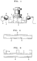
- FIG 1 Illustrated in FIG 1, is a simplified diagram of an ellipsometer as it is configured for use in the process of the present invention. It is contemplated that the process for controlling the removal of a film will be used in many different processes for thin film growth or etching of devices such as integrated circuits and other semiconductor and optical devices. However, the process of the present invention has been initially implemented in connection with the plasma etching of films upon a substrate and will be described in detail accordingly.
- a beam of incident light 10 is generated by the excitation head 20 of the ellipsometer 30.
- the light is generated from a light source (not shown) and transported to the head 20 via an optical fiber 25.
- the beam of light 10 is directed to strike a wafer 40.
- the excitation head 20 is positioned so that the angle of incidence 50 of the light beam 10 on the wafer 40 is about 70° from normal. Other angles of incidence are contemplated as useful depending upon the wafer. Angles of about 0° to about 90° are contemplated.
- the incident light 10 is reflected from the wafer 40.
- the light signal so reflected is detected by the detection head 60 of the ellipsometer 30.
- the detection head 60 transmits the optical signal to a monochromator via a an optical fiber (not pictured).
- the monochromator is used to select the desired wavelength of light, which is then transmitted to a detector.
- the detector converts the optical signal to an electrical signal and then transmits that signal to a signal processor, which determines the ⁇ and ⁇ values for the reflected light.
- the wafer 40 is placed in a chamber 70 in which the desired processing takes place.
- the chamber 70 depicted is suitable for plasma etching a film from the surface of the substrate.
- the chamber 70 is standard, except it is equipped with viewports 80 through which the ellipsometric signal enters and exits the chamber 70.
- the process of the present invention utilizes an ellipsometer for controlling the deposition and removal of films on substrates when there are patterned features with aspect ratios that are greater than 0.3 overlying the films, topography underlying the films or both patterned features over the film and topography under the film.
- the ellipsometer reports the values of ⁇ and ⁇ over time during a processing step in a device fabrication process. Since ⁇ and ⁇ are optical parameters of light reflected from the substrate, they are influenced by the optical path which the light must travel, i.e., through the layers on the substrate. As the thickness of these layers change, so do the values of ⁇ and ⁇ .
- ⁇ and ⁇ also change after a layer has been removed entirely from a portion of the wafer.
- An abrupt change in the slope of the trace of ⁇ and ⁇ over time during an etching step in a device fabrication process will indicate a change in the wafer surface, such as an interface between two materials.
- the process of the present invention achieves the desired degree of control by selecting a particular wavelength of light that provides a trace which is used for process control in the above described manner. Once the appropriate wavelength is selected, the ellipsometer is used to obtain traces of values of ⁇ and ⁇ over time during the process. If the appropriate wavelength of light has been selected, the trace will indicate when during the process an interface between two films is reached even though there is a mask overlying the film and/or topography underlying the film.
- the ellipsometric traces are referred to as signature traces, because they are substantially identical for a particular film etched under particular conditions. For example, if five wafers as illustrated in FIG. 2 were etched under substantially identical conditions, the traces obtained during the etch would be substantially identical as well. Thus, once a signature trace has been obtained for a particular wafer and process, the trace is used to control the processing of similar wafers in the same process. The traces also provide an indication that an interface is about to be reached during the process. This advance warning allows the process to be controlled with even greater accuracy.
- the wavelength of light used to generate the trace must be of a certain value. That wavelength is determined by considering a number of factors. Among these factors are: film thickness; the refractive index of the film material; the extinction coefficient of the film material at the relevant wavelength and the angle of incidence of the beam of light on the wafer surface.
- ⁇ and ⁇ are to be measured, the reflected light must be received by the detection head of the ellipsometer. Therefore, a wavelength must be selected such that the optical path through the layers is less than the absorption length of the light in those layers. The choice of wavelength is therefore dependent on the composition and thickness of the film or films being investigated.
- a wavelength is selected by using the following formula: wherein n ⁇ is the refractive index of the film being probed, k ⁇ is the extinction coefficient of the film material at the wavelength ⁇ , and ⁇ is the incident angle of the ellipsometric beam.
- the spectral refractive indices n ⁇ and extinction coefficients k ⁇ for the film materials are either obtained from reference data files or are determined experimentally using the ellipsometer to measure the spectrum of the blanket film. These values are also obtained in G. E. Jellison, Jr., "Optical Function of Silicon Determined by Two-channel Polarization Modulation Ellipsometry", Optical Materials , 1:46-47(1992) and Palik, D.
- n ⁇ and k ⁇ are selected for the top layer material.
- This formula provides a wavelength of light for which the absorption length through the particular film is much less than the optical path through the film. It is advantageous if the absorption length is a factor of about 5 to about 20 less than the optical path. It is particularly advantageous if the absorption length is at least a factor of 10 less than the optical path.
- the film on the substrate is a 2000 ⁇ -thick (d) film of polysilicon
- the following calculations are made to determine the appropriate wavelength: The above calculations illustrate that, for a 2000 ⁇ -thick film of polysilicon, a wavelength that would provide a useful trace is 375 nm or 428 nm, because at both wavelengths, the absorption length is much less than the optical path.
- the 632 nm wavelength is not useful because the absorption length is longer than the optical path. It is contemplated that, for multilayer films, the wavelength at which the trace is generated will be varied during the process to accommodate each of the individual films being deposited or removed.
- the wavelength it is also possible to select the wavelength by obtaining traces of a film during a process at a number of different wavelengths. By observing the traces obtained, the trace that indicates the interface with the desired degree of clarity is selected. The wavelength used to obtain that trace is then used to monitor the processing of subsequent films. The wavelength of the light used to generate the trace is varied from process to process and from film composition to film composition because the wavelength selected depends upon the characteristics of the film and the process. Therefore, it is advantageous if the ellipsometer used in the process is equipped with a broad spectral light source and a mechanism on the detector for selecting the desired wavelength of light to generate the desired trace.
- Example 1 Use of the Process of the Present Invention to Control a Plasma Etch
- the ellipsometer used to determine the ellipsometric parameters ( ⁇ , ⁇ ) was a UV-visible, phase modulated, spectroscopic ellipsometer made by the ISA division of Jobin-Yvon of Longjumeau, France.
- the ellipsometer was equipped with a white light source from a Xenon arc lamp. The light was polarized and passed through a phase modulator operating at 50 KHz.
- the excitation head of the ellipsometer was positioned such that the elliptically polarized light will hit a wafer at an angle of about 70° from normal.
- a detection head was mounted at -70° from normal.
- the wavelength of interest was observed by using a monochromator to exclude light of other wavelengths.
- the ellipsometer was used to monitor the etching of films on several different wafers.
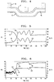
- One such film depicted in FIG. 2, was a 1000 ⁇ thick layer of titanium nitride 91 over a 2000 ⁇ thick layer of polysilicon 92 over a 70 ⁇ thick layer of an oxide of silicon 93.
- Another film depicted in FIG. 3, was the same film as depicted in FIG. 2 but with a 2000 ⁇ mask 94 of submicron features deposited thereover.
- a third film, as depicted in FIG. 4 is the film of FIG. 3, but deposited over a wafer with topography (not pictured) thereunder.
- the wafers were placed in an etching tool that was manufactured by Lucas Labs of Sunnyvale, California.
- the tool was configured for single wafer processing of 125 mm diameter wafers.
- the wafer was clamped to a chuck.
- the temperature of the wafer was controlled using backside cooling with a helium purge by controlling the temperature of the chuck at about 0°C.
- a low pressure, high density helicon plasma source also made by Lucas Labs, was used to generate the plasma, which consisted of ions, electrons and reactive neutrals.
- the wafer was placed in the reaction chamber into which a gas was introduced.
- the native oxide was removed by igniting a plasma with 100 sccm of HBr and 20 sccm of Cl2 at an rf-bias of 50 W for 10 seconds.
- the helicon source power was 2500 W and the reactor pressure was 2 mTorr.
- the flow of the Cl2 was shut off and the layer of titanium nitride was removed using the same conditions.
- the etchant recipe was changed by adding 20 sccm of a 20 percent/80 percent mixture of O2 and helium to the 100 sccm of HBr to etch the polysilicon layer.
- the plasma recipe was again changed by reducing the rf-bias from 50 W to 25 W to avoid etching the thin oxide layer beneath the polysilicon. This change was made about 10 seconds after the O2/helium was introduced.
- Ellipsometric traces were obtained while etching several wafers with the films described in FIGs. 2-4 deposited thereon.
- the ellipsometric traces were obtained using a monochromator to select various wavelengths to observe the effect of wavelength on the ellipsometric trace obtained.
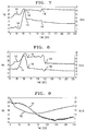
- a trace was obtained for a blanket film as illustrated in FIG. 2. This trace is illustrated in FIG. 5.
- the wavelength used to generate this trace was 632 nm. This wavelength is the wavelength used by single wavelength ellipsometers with a helium neon light source.
- the trace that was obtained indicates at what points in the process the first layer of titanium nitride and the second layer of polysilicon were removed. These points were indicated by abrupt changes in the slope of ⁇ 80 and ⁇ 90 over time during the process.
- the point in the process when the titanium nitride was removed is indicated by point 100 and the point in the process when the polysilicon was removed is illustrated by point 120.
- Such traces are useful for process control during device fabrication because, by observing the trace, one can change the conditions to which the film is subjected.
- FIG. 6 is another ellipsometric trace obtained while etching a film under the conditions described above.
- the film is again illustrated in FIG. 2.
- the wavelength of interest was selected by the process of the present invention. Again, the wavelength was obtained from the reflected light using a monochromator. The wavelength was 375 nm.
- the traces clearly indicated the points during the process when the first layer of titanium nitride 136 and the second layer of polysilicon 138 were removed. Again, these changes were indicated by an abrupt change in the slope of ⁇ 132 and ⁇ 134 over time during the process.
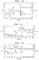
- FIGs. 7-9 are ellipsometric traces obtained while etching films described in FIG. 3 under the above-described conditions.
- the trace was obtained by first calculating the wavelength of interest to generate the trace using the method described above which was again 375 nm.
- the film had a silicon oxide mask thereover that was typical of masks used for integrated circuit fabrication.
- FIG. 8 illustrates the effect that a change in the wavelength used to generate the trace will have on the trace that is obtained.
- the trace was obtained while etching a film as illustrated in FIG. 3 under the conditions described above.
- the conditions were identical to the conditions under which the trace depicted in FIG. 7 was obtained.
- the only difference was that the wavelength used to generate the trace was 428 nm.
- FIG. 8 clearly indicates the points during the process when the titanium nitride 156 and the polysilicon 158 were removed. These points were again illustrated by abrupt changes in the slope of ⁇ 152 and ⁇ 154 over time during the process.
- FIGS. 7 and 8 illustrate that a range of appropriate wavelengths are provided by the above formula 1. This formula provides a mechanism to select a wavelength in the appropriate range. This wavelength is then increased or decreased, depending upon the requirements of a particular process. Once the appropriate wavelength is approximated, one skilled in the art will appreciate how much the wavelength will be increased or decreased in order to obtain specific processing objectives.
- FIG. 9 illustrates that, when processing films with a mask thereover, not every wavelength of light will provide a useful trace.
- the trace in FIG. 9 was obtained while etching a film as illustrated in FIG. 3 under the conditions described above.
- the mask 94 had an aspect ratio of 0.4 (2000 ⁇ high/5000 ⁇ wide).
- the wavelength of light used to generate the trace was 632 nm, a wavelength that is typically selected for performing ellipsometry.
- the trace obtained does not indicate at what points during the etch that the titanium nitride and polysilicon were removed because there is no point during the etch when the slope of ⁇ 162 and ⁇ 164 changed abruptly over time.
- the trace illustrated in FIG. 5 was also obtained at this wavelength. However, the trace in FIG. 5 does indicate when the interfaces were encountered during the process. This is due to the fact that the trace in FIG. 5 was obtained when etching a blanket film. Blanket films do not generate the same type of ellipsometric signals, nor do they provide the same degree of interference with these signals as do high aspect ratio masks and topography. Therefore, although a useful trace is obtained at a particular wavelength for a blanket film, that wavelength will not necessarily provide a useful trace for fabrication process control for patterned wafers. FIG. 9, therefore illustrates that the appropriate wavelength must be selected to obtain an ellipsometric trace that is useful for controlling a lithographic process when a mask is deposited on the wafer.
- a trace was obtained by etching a film as illustrated in FIG. 4 under the conditions described above.
- the wavelength of light used to generate the trace was 375 nm and was calculated as described above.
- the trace that was obtained is illustrated in FIG. 10.
- the trace clearly illustrates the points in the process when the titanium nitride 176 and the polysilicon 178 are removed from the wafer. These points are again indicated by an abrupt change in the slope of ⁇ 172 and ⁇ 174 over time.
- the process of the present invention is useful even if there is a mask or topography over the entire wafer surface.
- prior art ellipsometric processes required a large area with no mask and no topography in order to practice the ellipsometric technique.
- useful traces are obtained even if the mask is a series of submicron lines and spaces over the entire substrate surface.
- the lines in the mask used to obtain the trace depicted in FIG. 11 had an aspect ratio of about 1.
- the trace in FIG. 11 was obtained by etching a film as depicted generally in FIG. 3, wherein the mask was a series of submicron lines and spaces.
- the incident beam was in a direction that was parallel to the direction of the lines and spaces on the mask.
- the wavelength used to generate the trace was 375 nm and was calculated as described above.
- the trace obtained indicates the points during the etch when the titanium nitride 186 and the polysilicon 188 layers were removed from the wafer. However, this indication was provided only by the change in the rate at which the value of ⁇ 184 changed during the process. Therefore, the change in one of either optical parameter, ⁇ or ⁇ , will provide the information necessary for device fabrication process control.
- FIG. 12 was obtained under the identical conditions used to obtain the trace illustrated in FIG. 11, except that the direction of the incident beam of light was perpendicular to the direction of the lines and spaces on the mask overlying the film.
- FIG. 12 illustrates that the trace obtained under these conditions does indicate the points during the etch when the titanium nitride 196 and the polysilicon 198 were removed.
- the point in the process at which the titanium nitride was removed was indicated by the peak value of ⁇ 192 and the point at which the polysilicon was removed was indicated by the abrupt change in the slope of ⁇ 194.
- a signature trace is obtained for a particular film under particular conditions, that trace is used to control the processing of substantially identical films under substantially identical conditions. If the appropriate wavelength is selected, the point in the process between films will be indicated by a marked change in the value or slope of at least one of the ellipsometric angles ⁇ and ⁇ . The particular type of change will vary widely from trace to trace, however.
- the process of the present invention will be used to observe and control numerous aspects of device fabrication that require deposition or removal of materials over irregular surfaces.
- the process is used to control the deposition of films onto substrates in addition to controlling the removal of those films as described above.
- the process is used to control deposition much in the manner of the processes described in U.S. Patent No. 5,091,320 to Aspnes et al. and U.S. Patent No. 5,131,752 to Yu et al., both of which are incorporated by reference.
- the film will be grown under the dry deposition conditions described in Aspnes et al.
- the deposition of a multilayer film over topography or other surface irregularity is monitored and controlled by observing the trace being obtained in real time during the deposition process.
- the trace indicates the thickness of the first layer because the slope of ⁇ and/or ⁇ is relatively constant over a period of time. When that period of time has elapsed, the desired thickness has been deposited.
- the process conditions are then changed to begin depositing the second layer of film.
- the point in time when deposition of the second film begins is characterized by an abrupt change in the slope of ⁇ and/or ⁇ . This indicates the point during the process when the deposition begins for the second layer of film.
- the deposition of the second layer is controlled, because one can identify the point in time during the process when deposition of this layer commenced. From this information one can determine when the desired amount of material has been deposited by simply observing the length of time that elapses from the point during the process when deposition began. This observation cannot be made using a trace such as the one illustrated in FIG. 9, because no interface is indicated by the trace.
Landscapes
- Physics & Mathematics (AREA)
- Chemical & Material Sciences (AREA)
- Analytical Chemistry (AREA)
- Engineering & Computer Science (AREA)
- Plasma & Fusion (AREA)
- Biochemistry (AREA)
- Health & Medical Sciences (AREA)
- Life Sciences & Earth Sciences (AREA)
- Spectroscopy & Molecular Physics (AREA)
- General Health & Medical Sciences (AREA)
- General Physics & Mathematics (AREA)
- Immunology (AREA)
- Pathology (AREA)
- Drying Of Semiconductors (AREA)
- Polarising Elements (AREA)
- Testing Or Measuring Of Semiconductors Or The Like (AREA)
Applications Claiming Priority (2)
| Application Number | Priority Date | Filing Date | Title |
|---|---|---|---|
| US08/152,776 US5494697A (en) | 1993-11-15 | 1993-11-15 | Process for fabricating a device using an ellipsometric technique |
| US152776 | 1993-11-15 |
Publications (2)
| Publication Number | Publication Date |
|---|---|
| EP0653621A1 true EP0653621A1 (fr) | 1995-05-17 |
| EP0653621B1 EP0653621B1 (fr) | 2000-04-12 |
Family
ID=22544400
Family Applications (1)
| Application Number | Title | Priority Date | Filing Date |
|---|---|---|---|
| EP94308068A Expired - Lifetime EP0653621B1 (fr) | 1993-11-15 | 1994-11-02 | Procédé de fabrication d'un dispositif utilisant une technique ellipsométrique |
Country Status (5)
| Country | Link |
|---|---|
| US (1) | US5494697A (fr) |
| EP (1) | EP0653621B1 (fr) |
| JP (1) | JPH07183348A (fr) |
| KR (1) | KR100358265B1 (fr) |
| DE (1) | DE69423942T2 (fr) |
Cited By (5)
| Publication number | Priority date | Publication date | Assignee | Title |
|---|---|---|---|---|
| EP0768512A3 (fr) * | 1995-10-16 | 1998-10-21 | Lucent Technologies Inc. | Procédé de fabrication utilisant la lumière polarisée pour la détermination de l'épaisseur d'une couche mince |
| FR2771850A1 (fr) * | 1997-12-02 | 1999-06-04 | France Telecom | Procede de fabrication de dispositifs en couches minces utilisant la technique de la reflectance anisotrope |
| US6406641B1 (en) | 1997-06-17 | 2002-06-18 | Luxtron Corporation | Liquid etch endpoint detection and process metrology |
| US6868312B2 (en) * | 2000-08-10 | 2005-03-15 | L'air Liquide Societe Anonyme A Directoire Et Conseil De Surveillance Pour L'etude Et L'exploitation Des Procedes Georges Claude | Method for real-time control of the fabrication of a thin-film structure by ellipsometric measurement |
| US8709268B2 (en) | 2011-11-14 | 2014-04-29 | Spts Technologies Limited | Etching apparatus and methods |
Families Citing this family (27)
| Publication number | Priority date | Publication date | Assignee | Title |
|---|---|---|---|---|
| US5877032A (en) * | 1995-10-12 | 1999-03-02 | Lucent Technologies Inc. | Process for device fabrication in which the plasma etch is controlled by monitoring optical emission |
| US6059873A (en) * | 1994-05-30 | 2000-05-09 | Semiconductor Energy Laboratory Co., Ltd. | Optical processing method with control of the illumination energy of laser light |
| US5910021A (en) * | 1994-07-04 | 1999-06-08 | Yamaha Corporation | Manufacture of semiconductor device with fine pattens |
| US5552327A (en) * | 1994-08-26 | 1996-09-03 | North Carolina State University | Methods for monitoring and controlling deposition and etching using p-polarized reflectance spectroscopy |
| US5665214A (en) * | 1995-05-03 | 1997-09-09 | Sony Corporation | Automatic film deposition control method and system |
| US5871805A (en) * | 1996-04-08 | 1999-02-16 | Lemelson; Jerome | Computer controlled vapor deposition processes |
| US5702956A (en) * | 1996-08-26 | 1997-12-30 | Taiwan Semiconductor Manufactoring, Company Ltd | Test site and a method of monitoring via etch depths for semiconductor devices |
| US5717490A (en) * | 1996-10-17 | 1998-02-10 | Lsi Logic Corporation | Method for identifying order skipping in spectroreflective film measurement equipment |
| DE69735727T2 (de) * | 1997-01-27 | 2007-01-04 | Peter D. Louisville Haaland | Verfahren zur verminderung der reflexion von optischen substraten |
| US6172812B1 (en) | 1997-01-27 | 2001-01-09 | Peter D. Haaland | Anti-reflection coatings and coated articles |
| US5900644A (en) * | 1997-07-14 | 1999-05-04 | Taiwan Semiconductor Manufacturing Company, Ltd. | Test site and a method of monitoring via etch depths for semiconductor devices |
| US6483580B1 (en) * | 1998-03-06 | 2002-11-19 | Kla-Tencor Technologies Corporation | Spectroscopic scatterometer system |
| US6228277B1 (en) * | 1998-10-14 | 2001-05-08 | Lucent Technologies Inc. | Etch endpoint detection |
| US6475815B1 (en) * | 1998-12-09 | 2002-11-05 | Matsushita Electric Industrial Co., Ltd. | Method of measuring temperature, method of taking samples for temperature measurement and method for fabricating semiconductor device |
| US6214496B1 (en) * | 1999-03-29 | 2001-04-10 | Infineon Technologies North America Corp. | Method for reducing corner rounding in mask fabrication utilizing elliptical energy beam |
| US6636309B1 (en) * | 2001-07-27 | 2003-10-21 | J.A. Woollam Co. | Application of spectroscopic ellipsometry to in situ real time fabrication of multiple alternating high/low refractive index narrow bandpass optical filters |
| US6641746B2 (en) | 2001-09-28 | 2003-11-04 | Agere Systems, Inc. | Control of semiconductor processing |
| US6940592B2 (en) * | 2001-10-09 | 2005-09-06 | Applied Materials, Inc. | Calibration as well as measurement on the same workpiece during fabrication |
| US7280230B2 (en) * | 2001-12-19 | 2007-10-09 | Kla-Tencor Technologies Corporation | Parametric profiling using optical spectroscopic systems |
| US7216045B2 (en) * | 2002-06-03 | 2007-05-08 | Timbre Technologies, Inc. | Selection of wavelengths for integrated circuit optical metrology |
| US7006222B2 (en) * | 2003-01-08 | 2006-02-28 | Kla-Tencor Technologies Corporation | Concurrent measurement and cleaning of thin films on silicon-on-insulator (SOI) |
| DE10319843A1 (de) * | 2003-05-03 | 2004-12-02 | Infineon Technologies Ag | Verfahren zum Bestimmen der Tiefe einer vergrabenen Struktur |
| JP2005015885A (ja) * | 2003-06-27 | 2005-01-20 | Ebara Corp | 基板処理方法及び装置 |
| US7063991B1 (en) | 2004-07-28 | 2006-06-20 | Advanced Micro Devices, Inc. | Methods of determining characteristics of doped regions on device wafers, and system for accomplishing same |
| US7515253B2 (en) | 2005-01-12 | 2009-04-07 | Kla-Tencor Technologies Corporation | System for measuring a sample with a layer containing a periodic diffracting structure |
| DE102006012022A1 (de) * | 2006-03-14 | 2007-09-20 | Betriebsforschungsinstitut VDEh - Institut für angewandte Forschung GmbH | Verfahren zur Bestimmung der Auflage auf einem bewegten Metallband |
| US9147610B2 (en) | 2012-06-22 | 2015-09-29 | Infineon Technologies Ag | Monitor structures and methods of formation thereof |
Citations (1)
| Publication number | Priority date | Publication date | Assignee | Title |
|---|---|---|---|---|
| US5131752A (en) * | 1990-06-28 | 1992-07-21 | Tamarack Scientific Co., Inc. | Method for film thickness endpoint control |
Family Cites Families (15)
| Publication number | Priority date | Publication date | Assignee | Title |
|---|---|---|---|---|
| DE3473971D1 (en) * | 1984-06-20 | 1988-10-13 | Ibm | Method of standardization and stabilization of semiconductor wafers |
| US5087591A (en) * | 1985-01-22 | 1992-02-11 | Texas Instruments Incorporated | Contact etch process |
| US4874240A (en) * | 1988-03-01 | 1989-10-17 | Hoechst Celanese | Characterization of semiconductor resist material during processing |
| US5145554A (en) * | 1989-02-23 | 1992-09-08 | Seiko Epson Corporation | Method of anisotropic dry etching of thin film semiconductors |
| US5223914A (en) * | 1989-04-28 | 1993-06-29 | International Business Machines Corporation | Follow-up system for etch process monitoring |
| JPH047852A (ja) * | 1990-04-25 | 1992-01-13 | Fujitsu Ltd | 膜厚測定方法 |
| US5091320A (en) * | 1990-06-15 | 1992-02-25 | Bell Communications Research, Inc. | Ellipsometric control of material growth |
| US5362356A (en) * | 1990-12-20 | 1994-11-08 | Lsi Logic Corporation | Plasma etching process control |
| US5270222A (en) * | 1990-12-31 | 1993-12-14 | Texas Instruments Incorporated | Method and apparatus for semiconductor device fabrication diagnosis and prognosis |
| US5220403A (en) * | 1991-03-11 | 1993-06-15 | International Business Machines Corporation | Apparatus and a method for high numerical aperture microscopic examination of materials |
| US5208648A (en) * | 1991-03-11 | 1993-05-04 | International Business Machines Corporation | Apparatus and a method for high numerical aperture microscopic examination of materials |
| US5395769A (en) * | 1992-06-26 | 1995-03-07 | International Business Machines Corporation | Method for controlling silicon etch depth |
| WO1994002832A1 (fr) * | 1992-07-15 | 1994-02-03 | On-Line Technologies, Inc. | Procede et appareil de surveillance du traitement d'une couche |
| US5277747A (en) * | 1992-09-15 | 1994-01-11 | Bell Communications Research, Inc. | Extraction of spatially varying dielectric function from ellipsometric data |
| US5354575A (en) * | 1993-04-16 | 1994-10-11 | University Of Maryland | Ellipsometric approach to anti-reflection coatings of semiconductor laser amplifiers |
-
1993
- 1993-11-15 US US08/152,776 patent/US5494697A/en not_active Expired - Lifetime
-
1994
- 1994-11-02 DE DE69423942T patent/DE69423942T2/de not_active Expired - Fee Related
- 1994-11-02 EP EP94308068A patent/EP0653621B1/fr not_active Expired - Lifetime
- 1994-11-07 KR KR1019940029023A patent/KR100358265B1/ko not_active Expired - Lifetime
- 1994-11-14 JP JP6302650A patent/JPH07183348A/ja active Pending
Patent Citations (1)
| Publication number | Priority date | Publication date | Assignee | Title |
|---|---|---|---|---|
| US5131752A (en) * | 1990-06-28 | 1992-07-21 | Tamarack Scientific Co., Inc. | Method for film thickness endpoint control |
Non-Patent Citations (2)
| Title |
|---|
| M.HAVERLAG ET AL.: "In situ ellipsometry and reflectometry during etching of patterned surfaces: Experiments and simulations", JOURNAL OF VACUUM SCIENCE AND TECHNOLOGY: PART B, vol. 10, no. 6, November 1992 (1992-11-01), NEW YORK US, pages 2412 - 2418, XP000331696, DOI: doi:10.1116/1.586076 * |
| S.A.HENCK: "In situ spectral ellipsometry for real-time thickness measurement: Etching multilayer stacks", JOURNAL OF VACUUM SCIENCE AND TECHNOLOGY: PART A, vol. 11, no. 4, July 1993 (1993-07-01), NEW YORK US, pages 1179 - 1185, XP000403723, DOI: doi:10.1116/1.578490 * |
Cited By (7)
| Publication number | Priority date | Publication date | Assignee | Title |
|---|---|---|---|---|
| EP0768512A3 (fr) * | 1995-10-16 | 1998-10-21 | Lucent Technologies Inc. | Procédé de fabrication utilisant la lumière polarisée pour la détermination de l'épaisseur d'une couche mince |
| US6406641B1 (en) | 1997-06-17 | 2002-06-18 | Luxtron Corporation | Liquid etch endpoint detection and process metrology |
| FR2771850A1 (fr) * | 1997-12-02 | 1999-06-04 | France Telecom | Procede de fabrication de dispositifs en couches minces utilisant la technique de la reflectance anisotrope |
| EP0923121A1 (fr) * | 1997-12-02 | 1999-06-16 | France Telecom | Procédé de fabrication de dispositifs en couches minces utilisant la technique de la réflectance anisotrope |
| US6868312B2 (en) * | 2000-08-10 | 2005-03-15 | L'air Liquide Societe Anonyme A Directoire Et Conseil De Surveillance Pour L'etude Et L'exploitation Des Procedes Georges Claude | Method for real-time control of the fabrication of a thin-film structure by ellipsometric measurement |
| US8709268B2 (en) | 2011-11-14 | 2014-04-29 | Spts Technologies Limited | Etching apparatus and methods |
| US9640370B2 (en) | 2011-11-14 | 2017-05-02 | Spts Technologies Limited | Etching apparatus and methods |
Also Published As
| Publication number | Publication date |
|---|---|
| DE69423942T2 (de) | 2001-07-19 |
| KR950015627A (ko) | 1995-06-17 |
| JPH07183348A (ja) | 1995-07-21 |
| KR100358265B1 (ko) | 2003-02-19 |
| EP0653621B1 (fr) | 2000-04-12 |
| DE69423942D1 (de) | 2000-05-18 |
| US5494697A (en) | 1996-02-27 |
Similar Documents
| Publication | Publication Date | Title |
|---|---|---|
| EP0653621B1 (fr) | Procédé de fabrication d'un dispositif utilisant une technique ellipsométrique | |
| US5835221A (en) | Process for fabricating a device using polarized light to determine film thickness | |
| US6961131B2 (en) | Film thickness measuring method of member to be processed using emission spectroscopy and processing method of the member using the measuring method | |
| US5362356A (en) | Plasma etching process control | |
| US6489624B1 (en) | Apparatus and methods for detecting thickness of a patterned layer | |
| US7009715B2 (en) | Method and apparatus for determining endpoint of semiconductor element fabricating process and method and apparatus for processing member to be processed | |
| TWI711800B (zh) | 電漿處理方法、及電漿處理裝置 | |
| JP3854810B2 (ja) | 発光分光法による被処理材の膜厚測定方法及び装置とそれを用いた被処理材の処理方法及び装置 | |
| NL2000563C2 (nl) | Extraheren van gewone en buitengewone optische karakteristieken voor de meting van kritische afmetingen van anisotrope materialen. | |
| CN1217469A (zh) | 湿法腐蚀过程的终点探测方法 | |
| US6228277B1 (en) | Etch endpoint detection | |
| Lee et al. | Analysis of reflectometry and ellipsometry data from patterned structures | |
| US7092096B2 (en) | Optical scatterometry method of sidewall spacer analysis | |
| Maynard et al. | Plasma etching of submicron devices: in situ monitoring and control by multi-wavelength ellipsometry | |
| Vallon et al. | Real-time ultraviolet ellipsometry monitoring of gate patterning in a high-density plasma | |
| JP2000100797A (ja) | 素子の製造方法及び製造装置 | |
| KR100688478B1 (ko) | 반도체 웨이퍼 에칭 상태 계측방법 | |
| Ianno et al. | In situ spectroscopic ellipsometry studies of electron cyclotron resonance (ECR) plasma etching of oxides of silicon and GaAs | |
| KR100733120B1 (ko) | 반도체 웨이퍼처리의 검출방법 및 검출장치 | |
| KR100438379B1 (ko) | 반도체소자제조공정의 종점판정방법과 장치 및 그것을사용한 피처리재의 처리방법과 장치 | |
| JP4641890B2 (ja) | 測定方法、および半導体装置の製造方法 | |
| Reinhardt et al. | Use of beam profile reflectometry to determine depth of silicon etch damage and contamination | |
| KR20030072031A (ko) | 반도체 애싱설비의 스트립불량 감지장치 및 그 방법 | |
| JPH0567590A (ja) | 半導体装置のエツチングにおける終点検出方法 | |
| KR20030087804A (ko) | 반도체 애싱설비의 스트립불량 감지장치 및 그 방법 |
Legal Events
| Date | Code | Title | Description |
|---|---|---|---|
| PUAI | Public reference made under article 153(3) epc to a published international application that has entered the european phase |
Free format text: ORIGINAL CODE: 0009012 |
|
| AK | Designated contracting states |
Kind code of ref document: A1 Designated state(s): DE FR GB |
|
| RIN1 | Information on inventor provided before grant (corrected) |
Inventor name: LEE, TSENG-CHUNG Inventor name: IBBOTSON, DALE EDWARD Inventor name: BLAYO,NADINE |
|
| 17P | Request for examination filed |
Effective date: 19951102 |
|
| 17Q | First examination report despatched |
Effective date: 19980803 |
|
| GRAG | Despatch of communication of intention to grant |
Free format text: ORIGINAL CODE: EPIDOS AGRA |
|
| GRAG | Despatch of communication of intention to grant |
Free format text: ORIGINAL CODE: EPIDOS AGRA |
|
| GRAH | Despatch of communication of intention to grant a patent |
Free format text: ORIGINAL CODE: EPIDOS IGRA |
|
| GRAH | Despatch of communication of intention to grant a patent |
Free format text: ORIGINAL CODE: EPIDOS IGRA |
|
| GRAA | (expected) grant |
Free format text: ORIGINAL CODE: 0009210 |
|
| AK | Designated contracting states |
Kind code of ref document: B1 Designated state(s): DE FR GB |
|
| REF | Corresponds to: |
Ref document number: 69423942 Country of ref document: DE Date of ref document: 20000518 |
|
| ET | Fr: translation filed | ||
| PLBE | No opposition filed within time limit |
Free format text: ORIGINAL CODE: 0009261 |
|
| STAA | Information on the status of an ep patent application or granted ep patent |
Free format text: STATUS: NO OPPOSITION FILED WITHIN TIME LIMIT |
|
| 26N | No opposition filed | ||
| REG | Reference to a national code |
Ref country code: GB Ref legal event code: IF02 |
|
| PGFP | Annual fee paid to national office [announced via postgrant information from national office to epo] |
Ref country code: GB Payment date: 20071128 Year of fee payment: 14 Ref country code: FR Payment date: 20071119 Year of fee payment: 14 |
|
| PGFP | Annual fee paid to national office [announced via postgrant information from national office to epo] |
Ref country code: DE Payment date: 20071221 Year of fee payment: 14 |
|
| GBPC | Gb: european patent ceased through non-payment of renewal fee |
Effective date: 20081102 |
|
| REG | Reference to a national code |
Ref country code: FR Ref legal event code: ST Effective date: 20090731 |
|
| PG25 | Lapsed in a contracting state [announced via postgrant information from national office to epo] |
Ref country code: DE Free format text: LAPSE BECAUSE OF NON-PAYMENT OF DUE FEES Effective date: 20090603 |
|
| PG25 | Lapsed in a contracting state [announced via postgrant information from national office to epo] |
Ref country code: GB Free format text: LAPSE BECAUSE OF NON-PAYMENT OF DUE FEES Effective date: 20081102 |
|
| PG25 | Lapsed in a contracting state [announced via postgrant information from national office to epo] |
Ref country code: FR Free format text: LAPSE BECAUSE OF NON-PAYMENT OF DUE FEES Effective date: 20081130 |