EP0653783A2 - Verfahren zur Herstellung einer isolierenden Schicht - Google Patents
Verfahren zur Herstellung einer isolierenden Schicht Download PDFInfo
- Publication number
- EP0653783A2 EP0653783A2 EP94117440A EP94117440A EP0653783A2 EP 0653783 A2 EP0653783 A2 EP 0653783A2 EP 94117440 A EP94117440 A EP 94117440A EP 94117440 A EP94117440 A EP 94117440A EP 0653783 A2 EP0653783 A2 EP 0653783A2
- Authority
- EP
- European Patent Office
- Prior art keywords
- film
- forming
- siob
- bsg
- bsg film
- Prior art date
- Legal status (The legal status is an assumption and is not a legal conclusion. Google has not performed a legal analysis and makes no representation as to the accuracy of the status listed.)
- Withdrawn
Links
Images


Classifications
-
- H—ELECTRICITY
- H10—SEMICONDUCTOR DEVICES; ELECTRIC SOLID-STATE DEVICES NOT OTHERWISE PROVIDED FOR
- H10P—GENERIC PROCESSES OR APPARATUS FOR THE MANUFACTURE OR TREATMENT OF DEVICES COVERED BY CLASS H10
- H10P14/00—Formation of materials, e.g. in the shape of layers or pillars
- H10P14/60—Formation of materials, e.g. in the shape of layers or pillars of insulating materials
- H10P14/69—Inorganic materials
- H10P14/692—Inorganic materials composed of oxides, glassy oxides or oxide-based glasses
- H10P14/6921—Inorganic materials composed of oxides, glassy oxides or oxide-based glasses containing silicon
- H10P14/6922—Inorganic materials composed of oxides, glassy oxides or oxide-based glasses containing silicon the material containing Si, O and at least one of H, N, C, F or other non-metal elements, e.g. SiOC, SiOC:H or SiONC
- H10P14/6923—Inorganic materials composed of oxides, glassy oxides or oxide-based glasses containing silicon the material containing Si, O and at least one of H, N, C, F or other non-metal elements, e.g. SiOC, SiOC:H or SiONC the material being boron or phosphorus doped silicon oxides, e.g. BPSG, BSG or PSG
-
- C—CHEMISTRY; METALLURGY
- C03—GLASS; MINERAL OR SLAG WOOL
- C03C—CHEMICAL COMPOSITION OF GLASSES, GLAZES OR VITREOUS ENAMELS; SURFACE TREATMENT OF GLASS; SURFACE TREATMENT OF FIBRES OR FILAMENTS MADE FROM GLASS, MINERALS OR SLAGS; JOINING GLASS TO GLASS OR OTHER MATERIALS
- C03C3/00—Glass compositions
- C03C3/04—Glass compositions containing silica
- C03C3/076—Glass compositions containing silica with 40% to 90% silica, by weight
- C03C3/089—Glass compositions containing silica with 40% to 90% silica, by weight containing boron
-
- C—CHEMISTRY; METALLURGY
- C23—COATING METALLIC MATERIAL; COATING MATERIAL WITH METALLIC MATERIAL; CHEMICAL SURFACE TREATMENT; DIFFUSION TREATMENT OF METALLIC MATERIAL; COATING BY VACUUM EVAPORATION, BY SPUTTERING, BY ION IMPLANTATION OR BY CHEMICAL VAPOUR DEPOSITION, IN GENERAL; INHIBITING CORROSION OF METALLIC MATERIAL OR INCRUSTATION IN GENERAL
- C23C—COATING METALLIC MATERIAL; COATING MATERIAL WITH METALLIC MATERIAL; SURFACE TREATMENT OF METALLIC MATERIAL BY DIFFUSION INTO THE SURFACE, BY CHEMICAL CONVERSION OR SUBSTITUTION; COATING BY VACUUM EVAPORATION, BY SPUTTERING, BY ION IMPLANTATION OR BY CHEMICAL VAPOUR DEPOSITION, IN GENERAL
- C23C16/00—Chemical coating by decomposition of gaseous compounds, without leaving reaction products of surface material in the coating, i.e. chemical vapour deposition [CVD] processes
- C23C16/22—Chemical coating by decomposition of gaseous compounds, without leaving reaction products of surface material in the coating, i.e. chemical vapour deposition [CVD] processes characterised by the deposition of inorganic material, other than metallic material
- C23C16/30—Deposition of compounds, mixtures or solid solutions, e.g. borides, carbides, nitrides
- C23C16/40—Oxides
- C23C16/401—Oxides containing silicon
-
- H—ELECTRICITY
- H10—SEMICONDUCTOR DEVICES; ELECTRIC SOLID-STATE DEVICES NOT OTHERWISE PROVIDED FOR
- H10P—GENERIC PROCESSES OR APPARATUS FOR THE MANUFACTURE OR TREATMENT OF DEVICES COVERED BY CLASS H10
- H10P14/00—Formation of materials, e.g. in the shape of layers or pillars
- H10P14/60—Formation of materials, e.g. in the shape of layers or pillars of insulating materials
- H10P14/63—Formation of materials, e.g. in the shape of layers or pillars of insulating materials characterised by the formation processes
- H10P14/6326—Deposition processes
- H10P14/6328—Deposition from the gas or vapour phase
- H10P14/6334—Deposition from the gas or vapour phase using decomposition or reaction of gaseous or vapour phase compounds, i.e. chemical vapour deposition
-
- H—ELECTRICITY
- H10—SEMICONDUCTOR DEVICES; ELECTRIC SOLID-STATE DEVICES NOT OTHERWISE PROVIDED FOR
- H10P—GENERIC PROCESSES OR APPARATUS FOR THE MANUFACTURE OR TREATMENT OF DEVICES COVERED BY CLASS H10
- H10P14/00—Formation of materials, e.g. in the shape of layers or pillars
- H10P14/60—Formation of materials, e.g. in the shape of layers or pillars of insulating materials
- H10P14/66—Formation of materials, e.g. in the shape of layers or pillars of insulating materials characterised by the type of materials
- H10P14/668—Formation of materials, e.g. in the shape of layers or pillars of insulating materials characterised by the type of materials the materials being characterised by the deposition precursor materials
- H10P14/6681—Formation of materials, e.g. in the shape of layers or pillars of insulating materials characterised by the type of materials the materials being characterised by the deposition precursor materials the precursor containing a compound comprising Si
- H10P14/6684—Formation of materials, e.g. in the shape of layers or pillars of insulating materials characterised by the type of materials the materials being characterised by the deposition precursor materials the precursor containing a compound comprising Si the compound comprising silicon and oxygen
- H10P14/6686—Formation of materials, e.g. in the shape of layers or pillars of insulating materials characterised by the type of materials the materials being characterised by the deposition precursor materials the precursor containing a compound comprising Si the compound comprising silicon and oxygen the compound being a molecule comprising at least one silicon-oxygen bond and the compound having hydrogen or an organic group attached to the silicon or oxygen, e.g. a siloxane
-
- H—ELECTRICITY
- H10—SEMICONDUCTOR DEVICES; ELECTRIC SOLID-STATE DEVICES NOT OTHERWISE PROVIDED FOR
- H10P—GENERIC PROCESSES OR APPARATUS FOR THE MANUFACTURE OR TREATMENT OF DEVICES COVERED BY CLASS H10
- H10P14/00—Formation of materials, e.g. in the shape of layers or pillars
- H10P14/60—Formation of materials, e.g. in the shape of layers or pillars of insulating materials
- H10P14/69—Inorganic materials
- H10P14/692—Inorganic materials composed of oxides, glassy oxides or oxide-based glasses
- H10P14/6921—Inorganic materials composed of oxides, glassy oxides or oxide-based glasses containing silicon
- H10P14/6922—Inorganic materials composed of oxides, glassy oxides or oxide-based glasses containing silicon the material containing Si, O and at least one of H, N, C, F or other non-metal elements, e.g. SiOC, SiOC:H or SiONC
Definitions
- the present invention relates to a method for forming a borosilicate glass film (hereinafter referred to as a BSG film) by means of a CVD method.
- borosilicate glass film (BSG film) has been formed by means of a CVD method under the following conditions of gas and depositing temperature:
- the as-depo film according to the above CVD method is mixed with B2O3 + SiO2, and is not of glass structure.
- the as-depo means a state which is immediately after the formation.
- This film is poor in denseness and high in hygroscopicity.
- concentration of boron in the film exceeds 5 to 6 wt%, it abruptly becomes high in hygroscopicity. Therefore, it is not suitable for application to manufacturing process of a semiconductor device and the like.
- the film can be changed to a film of glass structure by heating the as-depo film at a high temperature of 800 °C or higher.
- An object of the invention is to provide a method for forming a film by which a BSG film with high denseness and low hygroscopicity can be obtained even immediately after the film has been formed at a low temperature.
- the inventors of the invention considered how an as-depo film of B2O3 + SiO2 is transformed to the film of glass structure by heat treatment at a high temperature. It led to a conclusion that bond of Si-O-B was formed due to a high temperature.
- a film forming method of the invention forms a BSG film, using a mixed gas which consists of an organometallic compound having bond of Si-O-B (SiOB source) and ozone (O3). With this, bond of Si-O-B is taken into the formed BSG film as its component as it is, and the as-depo BSG film has a glass structure. Accordingly, the as-depo BSG film is high in denseness and low in hygroscopicity.
- the SiOB source becomes easy to be decomposed due to using O3, it is possible to form a BSG film having Si-O-B bond in an as-depo state even in case that a depositing temperature is as low as 400 °C or lower.
- a film forming method of the invention can be applied to manufacturing process of a semiconductor device without being subject to restriction in its manufacturing process and without requiring some extra equipment or some extra time and labor.
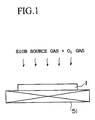
- Figure 1 is a cross-sectional view showing a state of forming a BSG film on the surface of a wafer according to the embodiment of the invention.
- Figures 2A to 2C are cross-sectional views showing a method for forming a BSG film as an interlayer insulating film to cover a lower interconnection layer according to the embodiment of the invention.
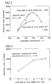
- Figure 3 is a characteristic diagram showing dependence of a deposition rate of a BSG film upon its depositing temperature according to the embodiment of the invention.
- Figure 4 is a characteristic diagram showing dependence of a deposition rate of a BSG film upon a flow rate of an SiOB gas according to the embodiment of the invention .
- Figure 5 is a characteristic diagram showing dependence of moisture content in an as-depo BSG film upon an additive ratio of O3 in O2 according to the embodiment of the invention.
- Figures 6 to 9 are diagrams showing general chemical formulas and constitutional formulas of organometallic compounds having Si-O-B bond according to the embodiment of the invention.
- An alkyl group is an atomic group obtained by removing one hydrogen atom from a paraffin hydrocarbon and is represented by a general chemical formula of C n H 2n+1 , and includes a methyl group (CH3), an ethyl group (C2H5), and the like.
- an aryl group is a generic name of the residual groups obtained by removing one hydrogen atom from the nucleus of aromatic hydrocarbon, and includes a phenyl group (C6H5-) and the like.
- This SiOB source has a boiling point of 184.5 °C, which is nearly equal to that of TEOS, and is a publicly known material very easy to use.
- a CVD method thermally decomposing the SiOB source gas at a temperature of 700°C or higher and a plasma-assisted CVD method are known as examples of CVD methods using an SiOB source gas having the SiOB source contained in a carrier gas.
- SiOB sources as represented by general chemical formulas and constitutional formulas as shown in Figures 6 to 9 instead of the above-mentioned SiOB source.
- a mixed gas obtained by adding ozone (O3) for oxidizing and decomposing the SiOB source to the above-mentioned SiOB source gas is used as a reactive gas in a CVD method.
- the SiOB source is promoted to be decomposed and can be thermally decomposed at a low temperature of 400°C or lower.
- a method for forming a BSG film on a semiconductor substrate by means of a CVD method using a mixed gas of the above-mentioned SiOB source and ozone (O3) according to an embodiment of the invention is described as referring to Figure 1 and Figures 2A to 2C.
- Figure 1 is a cross-sectional view showing a state of forming a BSG film on the surface of a wafer 1 on a wafer holder 51.
- Figures 2A to 2C are cross-sectional views showing a method for forming a BSG film 14 as an interlayer insulating film to cover a lower interconnection layer 13.
- the above-mentioned tris-trimethylsilylborate represented by a constitutional formula [(CH3)3SiO]3B is used as an SiOB source, and a mixed gas obtained by adding ozone (O3) to this tris-trimethylsilylborate [(CH3)3SiO]3B + O3 is used as a reaction gas.
- O3 is contained at a predetermined ratio in O2.
- a wafer (substrate) 1 is entered into a reaction chamber of an atmospheric pressure CVD apparatus, is set on a wafer holder 51 shown in Figure 1, and is heated as keeping its temperature at 400 °C or lower, provided that in the wafer 1 a ground insulating film 12 made of a silicon oxide film has been already formed on a semiconductor substrate 11 and furthermore a lower interconnection layer 13 made of an Al film has been formed on the backing insulating film 12.
- a mixed gas of an SiOB source gas having an SiOB source contained in such a carrier gas as N2 having a specified flow rate and O3 added by a specified additive ratio is introduced into the reaction chamber as a reaction gas.
- This gas-introducing state is kept for a specified time as shown in Figure 1.
- a BSG film 14 with specified thickness is formed on the wafer 1 as shown in Figure 2B.
- temperature of the wafer 1 is 400 °C or lower, it is possible to form an interlayer insulating film in a state where a lower interconnection layer 13 made of an Al film has been formed and to prevent the Al film from being subjected to a great thermal stress.
- the BSG film 14 formed in the above-mentioned manner was investigated for its film quality and other characteristics.
- the BSG film 14 formed in the above-mentioned manner proved to contain B of 15 to 18 mol% (equivalent to 5 to 6 wt%) in it.
- an Si/B ratio of the SiOB source is 3 and the ratio of B contained in the BSG film 14 is very near to its theoretical ratio (16.3 mol%).
- the B since the content of B contained in the BSG film 14 is determined almost according to an Si/B ratio in the SiOB source gas, the B can be doped accurately in concentration. And it is possible also to more finely adjust the concentration of B by adding TEOS.
- a BSG film containing so much B made by a film forming method of the prior art becomes nebular in its surface due to its moisture absorption immediately after forming the film, but on the other hand a BSG film according to this embodiment was very stable and did not absorbed moisture when it was left in the air for a short time. Furthermore, no abnormal state was found on the surface of the BSG film even after it was left in the air for a long time. It is thought that this is because the BSG film was improved in denseness by forming strong Si-O-B bond in it and so its moisture absorption was obstructed.
- the formed BSG film 14 has not only a stable film surface and good film quality as described above but also a high anti-crack ability.
- the BSG film 14 of about 3 um in thickness was crack-free.
- Figure 3 is a characteristic diagram showing dependence of a deposition rate of the film upon its depositing temperature.
- the axis of abscissas represents the depositing temperature(°C), and the axis of ordinates represents the deposition rate ( ⁇ /minute).
- the depositing temperature is in a range from 250°C to 400 °C, and other conditions are 4 SLM and 7 SLM in flow rate of the SiOB source gas and 6% in additive ratio of O3 in O2.
- the deposition rate is about 1000 ⁇ /minute and becomes greater as the temperature becomes higher, and reaches its maximum of about 4000 ⁇ /minute at the depositing temperature of 350°C, and after this it decreases as the temperature becomes still higher and becomes about 2500 ⁇ /minute at the depositing temperature of 400 °C.
- the flow rate of the SiOB source gas is 4 SLM, a trend similar to this appears and the deposition rate reaches its maximum of about 2600 ⁇ /minute at 350°C.
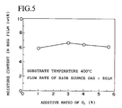
- Figure 4 is a characteristic diagram showing dependence of a deposition rate of the film upon a flow rate of the SiOB source gas.
- the axis of abscissas represents a flow rate of the SiOB source gas (SLM), and the axis of ordinates represents the deposition rate ( ⁇ /minute).
- the flow rate of the SiOB source gas is in a range from 2 SLM to 9 SLM, and other condition are 400°C in depositing temperature and 5.6 % in additive ratio of O3 in .
- the deposition rate is about 800 ⁇ /minute and becomes rapidly greater as the flow rate of the SiOB source gas becomes greater, and reaches about 1900 ⁇ /minute at 6 SLM in flow rate of the SiOB source gas, and after this the deposition rate increases gradually as the flow rate of the SiOB source gas becomes greater and it becomes about 2000 ⁇ /minute at 9 SLM in flow rate of the SiOB source gas.
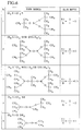
- Figure 5 is a characteristic diagram showing dependence of moisture content of the as-depo BSG film 14 upon an additive ratio of O3 in O2.
- the axis of abscissas represents the additive ratio of O3 (%), and the axis of ordinates represents the moisture content (wt%).
- the additive ratio of O3 in O2 is in a range from 1 % to 5.6 %, and other conditions are 400°C in depositing temperature and 8 SLM in flow rate of the SiOB source gas. In this case, the sample was left in the air for 6 hours after formation of the film till measurement of it.
- moisture content of the as-depo BSG film 14 proves to little depend upon an additive ratio of O3.
- a film forming method of the embodiment of the invention forms a BSG film 14, using a mixed gas of an organometallic compound having Si-O-B bond and ozone (O3).
- the as-depo BSG film 14 since the as-depo BSG film 14 has Si-O-B bond taken into it as a component of it as it is, the as-depo BSG film 14 comes to be of glass structure and results in being high in denseness and low in hygroscopicity.
- the SiOB source is made easier to be decomposed by using O3, it is possible to form a BSG film 14 having Si-O-B bond in an as-depo state even when depositing temperature is as low as 400 °C or lower.
- a film forming method of the embodiment of the invention can be applied to manufacturing process of a semiconductor device without restriction of materials used as the interconnection layer and without extra equipment or extra time and labor.
- the above-mentioned embodiment forms the BSG film 14 using a mixed gas of an organometallic compound having Si-O-B bond and ozone (O3), but it can also use another mixed gas obtained by adding tetra-ethylorthosilicate (TEOS) to these gases. By this, it is possible to adjust more finely the concentration of B in the BSG film to be formed.
- TEOS tetra-ethylorthosilicate
- the BSG film is formed by means of an atmospheric-pressure CVD method, but it can be also formed by means of a depressurized CVD method.
- the BSG film is formed on the interconnection layer made of Al, but it may be formed on an interconnection layer made of Al alloy containing at least one selected from group of Si, Cu and the like, other metal or a polycristalline silicon.
Landscapes
- Chemical & Material Sciences (AREA)
- Organic Chemistry (AREA)
- General Chemical & Material Sciences (AREA)
- Chemical Kinetics & Catalysis (AREA)
- Engineering & Computer Science (AREA)
- Materials Engineering (AREA)
- Mechanical Engineering (AREA)
- Metallurgy (AREA)
- Inorganic Chemistry (AREA)
- Life Sciences & Earth Sciences (AREA)
- Geochemistry & Mineralogy (AREA)
- Formation Of Insulating Films (AREA)
- Internal Circuitry In Semiconductor Integrated Circuit Devices (AREA)
Applications Claiming Priority (2)
| Application Number | Priority Date | Filing Date | Title |
|---|---|---|---|
| JP5281157A JPH0817173B2 (ja) | 1993-11-10 | 1993-11-10 | 成膜方法 |
| JP281157/93 | 1993-11-10 |
Publications (2)
| Publication Number | Publication Date |
|---|---|
| EP0653783A2 true EP0653783A2 (de) | 1995-05-17 |
| EP0653783A3 EP0653783A3 (de) | 1996-04-24 |
Family
ID=17635154
Family Applications (1)
| Application Number | Title | Priority Date | Filing Date |
|---|---|---|---|
| EP94117440A Withdrawn EP0653783A3 (de) | 1993-11-10 | 1994-11-04 | Verfahren zur Herstellung einer isolierenden Schicht. |
Country Status (3)
| Country | Link |
|---|---|
| US (1) | US5532193A (de) |
| EP (1) | EP0653783A3 (de) |
| JP (1) | JPH0817173B2 (de) |
Families Citing this family (11)
| Publication number | Priority date | Publication date | Assignee | Title |
|---|---|---|---|---|
| US7067442B1 (en) * | 1995-12-26 | 2006-06-27 | Micron Technology, Inc. | Method to avoid threshold voltage shift in thicker dielectric films |
| US6462394B1 (en) | 1995-12-26 | 2002-10-08 | Micron Technology, Inc. | Device configured to avoid threshold voltage shift in a dielectric film |
| US6114216A (en) * | 1996-11-13 | 2000-09-05 | Applied Materials, Inc. | Methods for shallow trench isolation |
| US6190955B1 (en) * | 1998-01-27 | 2001-02-20 | International Business Machines Corporation | Fabrication of trench capacitors using disposable hard mask |
| JP2994616B2 (ja) * | 1998-02-12 | 1999-12-27 | キヤノン販売株式会社 | 下地表面改質方法及び半導体装置の製造方法 |
| US6846739B1 (en) * | 1998-02-27 | 2005-01-25 | Micron Technology, Inc. | MOCVD process using ozone as a reactant to deposit a metal oxide barrier layer |
| US6136703A (en) * | 1998-09-03 | 2000-10-24 | Micron Technology, Inc. | Methods for forming phosphorus- and/or boron-containing silica layers on substrates |
| JP3251554B2 (ja) * | 1998-12-04 | 2002-01-28 | キヤノン販売株式会社 | 成膜方法及び半導体装置の製造方法 |
| JP2002274871A (ja) * | 2001-03-15 | 2002-09-25 | Asahi Denka Kogyo Kk | 光導波用珪酸系ガラス層の製造方法及びこれに用いられるcvd原料 |
| JP4329445B2 (ja) | 2003-08-04 | 2009-09-09 | セイコーエプソン株式会社 | 電気光学装置並びに電子機器 |
| DE102013223771B4 (de) | 2012-12-28 | 2023-07-06 | Volkswagen Aktiengesellschaft | Verfahren zur Vermessung eines axialen Bauraums |
Family Cites Families (6)
| Publication number | Priority date | Publication date | Assignee | Title |
|---|---|---|---|---|
| NL161306C (nl) * | 1971-05-28 | 1980-01-15 | Fujitsu Ltd | Werkwijze voor de vervaardiging van veldeffecttransis- toren met geisoleerde stuurelektrode. |
| US4892753A (en) * | 1986-12-19 | 1990-01-09 | Applied Materials, Inc. | Process for PECVD of silicon oxide using TEOS decomposition |
| US5104482A (en) * | 1989-02-21 | 1992-04-14 | Lam Research Corporation | Simultaneous glass deposition and viscoelastic flow process |
| JPH0766919B2 (ja) * | 1991-02-20 | 1995-07-19 | 株式会社半導体プロセス研究所 | 半導体製造装置 |
| JPH0782999B2 (ja) * | 1991-04-15 | 1995-09-06 | 株式会社半導体プロセス研究所 | 気相成長膜の形成方法、半導体製造装置、および半 導体装置 |
| EP0572704B1 (de) * | 1992-06-05 | 2000-04-19 | Semiconductor Process Laboratory Co., Ltd. | Verfahren zur Herstellung einer Halbleiteranordnung mittels eines Verfahren zur Reformierung einer Isolationsschicht die bei niederiger Temperatur durch CVD hergestellt ist |
-
1993
- 1993-11-10 JP JP5281157A patent/JPH0817173B2/ja not_active Expired - Fee Related
-
1994
- 1994-10-31 US US08/331,737 patent/US5532193A/en not_active Expired - Lifetime
- 1994-11-04 EP EP94117440A patent/EP0653783A3/de not_active Withdrawn
Non-Patent Citations (1)
| Title |
|---|
| JOURNAL OF THE ELECTROCHEMICAL SOCIETY, vol. 138, no. 10, 1 October 1991 pages 3019-3024, XP 000248007 FUJINO K ET AL 'DOPED SILICON OXIDE DEPOSITION BY ATMOSPHERIC PRESSURE AND LOW TEMPERATURE CHEMICAL VAPOR DEPOSITION USING TETRAETHOXYSILANE AND OZONE' * |
Also Published As
| Publication number | Publication date |
|---|---|
| JPH0817173B2 (ja) | 1996-02-21 |
| EP0653783A3 (de) | 1996-04-24 |
| JPH07135204A (ja) | 1995-05-23 |
| US5532193A (en) | 1996-07-02 |
Similar Documents
| Publication | Publication Date | Title |
|---|---|---|
| US5354387A (en) | Boron phosphorus silicate glass composite layer on semiconductor wafer | |
| US5204141A (en) | Deposition of silicon dioxide films at temperatures as low as 100 degree c. by lpcvd using organodisilane sources | |
| CN111041456B (zh) | 用于形成含硅和氧的薄膜的汽相沉积方法 | |
| KR102380197B1 (ko) | SiCON의 저온 분자층 증착 | |
| US5866205A (en) | Process for titanium nitride deposition using five- and six-coordinate titanium complexes | |
| KR100560654B1 (ko) | 질화실리콘막을 형성을 위한 질소화합물 및 이를 이용한질화실리콘 막의 형성방법 | |
| JP5031987B2 (ja) | 耐酸化性が良好な次世代ダマシンバリヤ適用のための二層膜 | |
| US20060084283A1 (en) | Low temperature sin deposition methods | |
| EP0421203B1 (de) | Integrierte Schaltungsstruktur mit einer zusammengesetzten Borphosphorsilikatglasschicht auf einer Halbleiterscheibe und verbesserte Herstellungsmethode dafür | |
| WO2004010467A2 (en) | Low temperature dielectric deposition using aminosilane and ozone | |
| CN103843118A (zh) | 用于半导体整合的不敏感干法移除工艺 | |
| KR20090130359A (ko) | 유기아미노실란 전구체로부터 산화규소 막을 형성시키는 방법 | |
| US5532193A (en) | Method for forming insulating film | |
| US5763021A (en) | Method of forming a dielectric film | |
| EP0711846A1 (de) | Titannitrid hergestellt mittels CVD | |
| US5324539A (en) | Method for forming CVD thin glass films | |
| JPS61502616A (ja) | 改良されたシリコンオキシニトリド材料及びその製造方法 | |
| US4546016A (en) | Deposition of borophosphosilicate glass | |
| JP2023529205A (ja) | 蒸着前駆体化合物及び使用のプロセス | |
| EP0932188A3 (de) | Abscheidung von Glas über eine Halbleiterscheibe | |
| US5569499A (en) | Method for reforming insulating film | |
| KR20240158300A (ko) | 규소-풍부 질화규소 필름의 제조 방법 | |
| Maxwell Jr et al. | Densification of SIPOS | |
| US6429149B1 (en) | Low temperature LPCVD PSG/BPSG process | |
| TW202532675A (zh) | 含碳氮化硼膜之成膜方法 |
Legal Events
| Date | Code | Title | Description |
|---|---|---|---|
| PUAI | Public reference made under article 153(3) epc to a published international application that has entered the european phase |
Free format text: ORIGINAL CODE: 0009012 |
|
| AK | Designated contracting states |
Kind code of ref document: A2 Designated state(s): DE FR GB IT NL |
|
| RIN1 | Information on inventor provided before grant (corrected) |
Inventor name: TOKUMASU, NOBORU C/O SEMICONDUCTOR PROCESS LAB. Inventor name: YUYAMA, YOSHIAKI C/O SEMICONDUCTOR PROCESS LAB. Inventor name: MAEDA, KAZUO C/O SEMICONDUCTOR PROCESS LABORATORY |
|
| PUAL | Search report despatched |
Free format text: ORIGINAL CODE: 0009013 |
|
| AK | Designated contracting states |
Kind code of ref document: A3 Designated state(s): DE FR GB IT NL |
|
| STAA | Information on the status of an ep patent application or granted ep patent |
Free format text: STATUS: THE APPLICATION IS DEEMED TO BE WITHDRAWN |
|
| 18D | Application deemed to be withdrawn |
Effective date: 19961025 |