EP0653786A2 - Verfahren zur Herstellung einer Halbleiteranordnung - Google Patents
Verfahren zur Herstellung einer Halbleiteranordnung Download PDFInfo
- Publication number
- EP0653786A2 EP0653786A2 EP94116726A EP94116726A EP0653786A2 EP 0653786 A2 EP0653786 A2 EP 0653786A2 EP 94116726 A EP94116726 A EP 94116726A EP 94116726 A EP94116726 A EP 94116726A EP 0653786 A2 EP0653786 A2 EP 0653786A2
- Authority
- EP
- European Patent Office
- Prior art keywords
- type
- forming
- region
- conduction type
- gate electrode
- Prior art date
- Legal status (The legal status is an assumption and is not a legal conclusion. Google has not performed a legal analysis and makes no representation as to the accuracy of the status listed.)
- Withdrawn
Links
Images










Classifications
-
- H—ELECTRICITY
- H10—SEMICONDUCTOR DEVICES; ELECTRIC SOLID-STATE DEVICES NOT OTHERWISE PROVIDED FOR
- H10D—INORGANIC ELECTRIC SEMICONDUCTOR DEVICES
- H10D30/00—Field-effect transistors [FET]
- H10D30/01—Manufacture or treatment
- H10D30/021—Manufacture or treatment of FETs having insulated gates [IGFET]
- H10D30/0221—Manufacture or treatment of FETs having insulated gates [IGFET] having asymmetry in the channel direction, e.g. lateral high-voltage MISFETs having drain offset region or extended-drain MOSFETs [EDMOS]
-
- H—ELECTRICITY
- H10—SEMICONDUCTOR DEVICES; ELECTRIC SOLID-STATE DEVICES NOT OTHERWISE PROVIDED FOR
- H10D—INORGANIC ELECTRIC SEMICONDUCTOR DEVICES
- H10D30/00—Field-effect transistors [FET]
- H10D30/01—Manufacture or treatment
- H10D30/021—Manufacture or treatment of FETs having insulated gates [IGFET]
- H10D30/028—Manufacture or treatment of FETs having insulated gates [IGFET] of double-diffused metal oxide semiconductor [DMOS] FETs
-
- H—ELECTRICITY
- H10—SEMICONDUCTOR DEVICES; ELECTRIC SOLID-STATE DEVICES NOT OTHERWISE PROVIDED FOR
- H10D—INORGANIC ELECTRIC SEMICONDUCTOR DEVICES
- H10D30/00—Field-effect transistors [FET]
- H10D30/60—Insulated-gate field-effect transistors [IGFET]
- H10D30/601—Insulated-gate field-effect transistors [IGFET] having lightly-doped drain or source extensions, e.g. LDD IGFETs or DDD IGFETs
- H10D30/603—Insulated-gate field-effect transistors [IGFET] having lightly-doped drain or source extensions, e.g. LDD IGFETs or DDD IGFETs having asymmetry in the channel direction, e.g. lateral high-voltage MISFETs having drain offset region or extended drain IGFETs [EDMOS]
-
- H—ELECTRICITY
- H10—SEMICONDUCTOR DEVICES; ELECTRIC SOLID-STATE DEVICES NOT OTHERWISE PROVIDED FOR
- H10D—INORGANIC ELECTRIC SEMICONDUCTOR DEVICES
- H10D30/00—Field-effect transistors [FET]
- H10D30/60—Insulated-gate field-effect transistors [IGFET]
- H10D30/64—Double-diffused metal-oxide semiconductor [DMOS] FETs
- H10D30/65—Lateral DMOS [LDMOS] FETs
-
- H—ELECTRICITY
- H10—SEMICONDUCTOR DEVICES; ELECTRIC SOLID-STATE DEVICES NOT OTHERWISE PROVIDED FOR
- H10D—INORGANIC ELECTRIC SEMICONDUCTOR DEVICES
- H10D84/00—Integrated devices formed in or on semiconductor substrates that comprise only semiconducting layers, e.g. on Si wafers or on GaAs-on-Si wafers
- H10D84/01—Manufacture or treatment
- H10D84/0107—Integrating at least one component covered by H10D12/00 or H10D30/00 with at least one component covered by H10D8/00, H10D10/00 or H10D18/00, e.g. integrating IGFETs with BJTs
- H10D84/0109—Integrating at least one component covered by H10D12/00 or H10D30/00 with at least one component covered by H10D8/00, H10D10/00 or H10D18/00, e.g. integrating IGFETs with BJTs the at least one component covered by H10D12/00 or H10D30/00 being a MOS device
-
- H—ELECTRICITY
- H10—SEMICONDUCTOR DEVICES; ELECTRIC SOLID-STATE DEVICES NOT OTHERWISE PROVIDED FOR
- H10D—INORGANIC ELECTRIC SEMICONDUCTOR DEVICES
- H10D84/00—Integrated devices formed in or on semiconductor substrates that comprise only semiconducting layers, e.g. on Si wafers or on GaAs-on-Si wafers
- H10D84/01—Manufacture or treatment
- H10D84/02—Manufacture or treatment characterised by using material-based technologies
- H10D84/03—Manufacture or treatment characterised by using material-based technologies using Group IV technology, e.g. silicon technology or silicon-carbide [SiC] technology
- H10D84/038—Manufacture or treatment characterised by using material-based technologies using Group IV technology, e.g. silicon technology or silicon-carbide [SiC] technology using silicon technology, e.g. SiGe
-
- H—ELECTRICITY
- H10—SEMICONDUCTOR DEVICES; ELECTRIC SOLID-STATE DEVICES NOT OTHERWISE PROVIDED FOR
- H10D—INORGANIC ELECTRIC SEMICONDUCTOR DEVICES
- H10D62/00—Semiconductor bodies, or regions thereof, of devices having potential barriers
- H10D62/10—Shapes, relative sizes or dispositions of the regions of the semiconductor bodies; Shapes of the semiconductor bodies
- H10D62/13—Semiconductor regions connected to electrodes carrying current to be rectified, amplified or switched, e.g. source or drain regions
- H10D62/149—Source or drain regions of field-effect devices
- H10D62/151—Source or drain regions of field-effect devices of IGFETs
-
- H—ELECTRICITY
- H10—SEMICONDUCTOR DEVICES; ELECTRIC SOLID-STATE DEVICES NOT OTHERWISE PROVIDED FOR
- H10D—INORGANIC ELECTRIC SEMICONDUCTOR DEVICES
- H10D62/00—Semiconductor bodies, or regions thereof, of devices having potential barriers
- H10D62/10—Shapes, relative sizes or dispositions of the regions of the semiconductor bodies; Shapes of the semiconductor bodies
- H10D62/17—Semiconductor regions connected to electrodes not carrying current to be rectified, amplified or switched, e.g. channel regions
- H10D62/393—Body regions of DMOS transistors or IGBTs
-
- H—ELECTRICITY
- H10—SEMICONDUCTOR DEVICES; ELECTRIC SOLID-STATE DEVICES NOT OTHERWISE PROVIDED FOR
- H10D—INORGANIC ELECTRIC SEMICONDUCTOR DEVICES
- H10D64/00—Electrodes of devices having potential barriers
- H10D64/20—Electrodes characterised by their shapes, relative sizes or dispositions
- H10D64/27—Electrodes not carrying the current to be rectified, amplified, oscillated or switched, e.g. gates
- H10D64/311—Gate electrodes for field-effect devices
- H10D64/411—Gate electrodes for field-effect devices for FETs
- H10D64/511—Gate electrodes for field-effect devices for FETs for IGFETs
- H10D64/514—Gate electrodes for field-effect devices for FETs for IGFETs characterised by the insulating layers
- H10D64/516—Gate electrodes for field-effect devices for FETs for IGFETs characterised by the insulating layers the thicknesses being non-uniform
Definitions
- the present invention relates to a low withstand voltage BiCMOS processing technique for mounting a power DMOS transistor, a bipolar transistor and a CMOS transistor on a common chip (the same base plate) and, more specifically, the present invention relates to a manufacturing method for the power DMOS transistor.
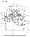
- Figure 18 shows a typical CMOS portion (a complementary insulated-gate field effect transistor) of a BiCMOS semiconductor apparatus which has a double-well (twin-tub) structure.
- the CMOS portion is comprised of an N+-type buried layer 2 formed on a P-type substrate 1; N-type epitaxial layer 3 grown over the buried layer 2; an isolated element island isolated by a P+-type isolation layer 4 which reaches the P-type substrate 1; and double wells (a P-type well 5 and an N-type well 6) formed in the isolated element island by ion-implantation and subsequent diffusion.
- a CMOS transistor is formed in the CMOS portion through the following steps.
- An active region is covered, for example, by a nitride film, and then element-isolating insulative film (local oxidation film : LOCOS) 7 is formed on the P+-type isolation layer 4 and the non-well portions between the P- and N-type wells 5 and 6 by selectively oxidizing the nitride film 7.
- An ion-implanted layer 8 is formed by implanting acceptor type (P-type) impurities such as BF2 shallowly from the major faces of the wells 5 and 6.
- P-type acceptor type
- Poly-silicon gate electrodes 10 are formed on the gate insulation film 9 deposited on the wells 5 and 6.
- An N+-type source region 11 NS and an N+-type drain region 11 ND are formed by self-alignment using the gate electrode 10 on the P-type well 5 as a mask.
- an N+-type well-contact region 11 NCON is formed simultaneously on the source side in the N-type well 6.
- a P+-type source region 11 PS and a P+-type drain region 11 PD are formed by the self-alignment technique using the gate electrode 10 on the N-type well 6 as a mask.
- a P+-type well-contact region 11 PCON is formed simultaneously on the source side in the P-type well 5.
- inter-layer insulation film 12 is formed, and, finally, source electrodes 13 NS , 13 PS and drain electrodes 13 ND , 13 PD , which fill contact holes punched through the insulation film 12 are deposited.
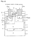
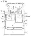
- Figures 19 and 20 show structures of a high-withstand voltage DMOS portion (double-diffusion type insulated gate field effect transistor) as a power MOS portion of the BiCMOS semiconductor apparatus.
- a P-type well 5 and an N-type well 6 of the N-channel type DMOSFET shown in Fig. 19 are formed through similar processes to those for the CMOS portion.
- the N-type well 6 constitutes an offset region which functions as an expanded drain for reducing ON-resistance of the MOSFET.
- An active region is covered, for example, by a nitride film, and then element-isolating insulative film (local oxidation film LOCOS) 7 is formed over the P+-type isolation layer 4 and thick local oxidation film 7a on the P-type well side on the N-type well 6 by selectively oxidizing the nitride film.
- An ion-implanted layer 8 is formed by implanting acceptor type (P-type) impurities such as BF2 shallowly from a major face of the P-type well 5.
- a gate electrode 10 is formed on gate insulation film 9 deposited on the P-type wells 5.
- a P-type base region (channel diffusion region) 21 is self-aligned in the P-type well 5 more deeply than the diffusion depth of the ion-implanted layer 8 by employing a process for forming a P-type base region of a bipolar transistor (NPN transistor) described later and by using the gate electrode 10 as a mask. Then, an N+-type source region 22 NS is formed from a major face side of the P-type base region 21 by employing the process for forming the N+- drain and source of the CMOS portion and by double diffusion using the gate electrode 10 as a mask, and an N+-type well-contact (drain) region 22 NCON from a major face of the N-type well 6.
- NPN transistor bipolar transistor
- Inter-layer insulation film 12 is formed, and, finally, a source electrode 23 NS and a drain electrode 23 ND which fill contact holes punched through the insulation film 12 are deposited.
- the thick local oxidation film 7a contributes to provision of higher withstand voltage by relaxing electric field convergence onto the edge of the drain.
- a P-type well 5 and an N-type well 6 of the P-channel type DMOSFET of the DMOS portion shown in Fig. 20 are formed through similar processes to those for the CMOS portion and the P-type well 5 constitutes an offset region which functions as an expanded drain for reducing ON-resistance of the MOSFET.
- an active region is covered, for example, by a nitride film, and then element-isolating insulative film 7 is formed on the P+-type isolation layer 4 and thick local oxidation film 7a on the N-type well side on the P-type well 5 by selectively oxidizing the nitride film.
- An ion-implanted layer 8 is formed by implanting acceptor type (P-type) impurities such as BF2 shallowly from a major face of the N-type well 6.
- a gate electrode 10 is formed on the gate insulation film 9 deposited on the N-type wells 6.
- a P+-type source region 22 PS is self-aligned in the N-type well 6 from its major face more deeply than the diffusion depth of the ion-implanted layer 8 by employing the process for forming the p+-type source and drain of the CMOS portion and by using the gate electrode 10 as a mask, and P+-type well-contact region 22 PCON in the P-type well 5.
- inter-layer insulation film 12 is formed, and finally, a source electrode 23 PS and a drain electrode 23 PD which fill contact holes punched through the insulation film 12 are deposited.
- the thick local oxidation film 7a contributes to provision of higher withstand voltage by relaxing electric field convergence onto the edge of the drain.
- the bipolar transistor portion of the BiCMOS semiconductor apparatus is comprised of a vertical NPN transistor and a transverse PNP transistor as shown in Fig. 21.
- the bipolar transistor portion is formed through processing steps similar to those for forming the CMOS portion as follows. At first, an N+-type buried layer 2 is formed on a P-type substrate 1. An N-type epitaxial layer 3 is grown over the buried layer 2, and then, a P+-type element isolation layer 4 which reaches the substrate 1 is formed to isolate an element island.
- a P-type base region 31 PB is formed in the N-type epitaxial layer 3, and then, an N+-type emitter region 32 NE and an N+-type collector region (collector-contact region) 32 NC are formed by employing the process for forming the N+-type source and drain of the CMOS portion.
- a base electrode 33 B After forming inter-layer insulation film 12, a base electrode 33 B , an emitter electrode 33 E , and a collector electrode 33 C , which fill contact holes punched through the insulation film 12, are formed.
- a P-type emitter region 31 PE and a P-type collector region 31 PC are formed in the N-type epitaxial layer 3 by employing the process for forming the P-type base region 31 PB of the vertical transistor, and then, N+-type base region (base-contact) 32 NB is formed by employing the process for forming the N+-type source and drain of the CMOS portion. Then, after forming inter-layer insulation film 12, a base electrode 34 B , an emitter electrode 34 E , and a collector electrode 34 C , which fill contact holes punched through the insulation film 12, are formed.
- the N-channel DMOSFET with double-well structure shown in Fig. 19, which functions as the power DMOS portion, may be constructed in a DMOS structure shown in Fig. 22 from which the P-type well 5 and the ion-implanted layer 8 are eliminated.
- an N+-type buried layer 2 is formed on a P-type substrate 1.
- An N-type epitaxial layer 3 is grown over the buried layer 2, and then, a P+-type element isolation layer 4 which reaches the substrate 1 is formed to isolate an element island.
- An N-type well 6 is formed in the isolated element island by ion-implantation and subsequent diffusion.
- the N-type well 6 functions as an offset region as an expanded drain for reducing ON-resistance of the MOSFET. Then, an active region is covered, for example, by a nitride film, and element-isolating insulative film 7 is formed on the P+-type isolation layer 4 and thick local oxidation film 7a is formed on the edge portion of the N-type well 6 by selectively oxidizing the nitride film.
- a gate electrode 10 is formed on gate insulation film 9 deposited on the N-type epitaxial layer 3.
- P-type base region (channel diffusion region) 21 is formed, as described earlier, by employing the process for forming the P-type base of the bipolar transistor (NPN transistor), by implanting impurity ions from a major face of the N-type epitaxial layer 3 by the self-alignment technique using the gate electrode 10 as a mask, and by subsequent heat treatment between 1000 and 1200 °C.
- NPN transistor bipolar transistor
- an N+-type source region 22 NS is formed from a major face of the P-type base region 21 by employing the process for forming the N+-type drain and source of the CMOS portion, and by ion-implantation using the gate electrode 10 as a mask followed by subsequent double diffusion.
- an N+-type well-contact region 22 Ncon is formed from a major face of the N-type well 6. Then, after depositing inter-layer insulation film 12, a source 23 NS and a drain electrode23 ND , which fill contact holes punched through the insulation film 12, are formed. Finally, a passivation film is deposited.
- the thick local oxidation film 7a contributes to provision of higher withstand voltage by relaxing electric field convergence onto the edge of the drain.
- the BiCMOS structure according to the prior art which is comprised of the above described DMOS portion as the power MOS portion accompanies following problems.
- ion-implanted layers 8 are formed by employing the ion-implantation process for forming the ion-implanted layer of the low-withstand voltage CMOS. Since ion-implantation process exclusive for forming an ion-implanted layer of the DMOS portions is not employed, the P-type ion-implanted layers 8, especially that of the N-channel MOSFET shown in Fig. 19, tend to suffer from insufficient withstand voltage caused by surface punching through because of deficit in total acceptor amount. Elongated channel length for avoiding this problem increases ON-resistance, which is hazardous for increasing current capacity. Withstand voltage increase and ON-resistance decrease are in trade-off relation to each other.
- the P-type base region 21 is formed by ion-implantation from the major face of the N-type epitaxial layer 3 using the gate electrode 10 as a mask for self-alignment and by heat treatment at high temperature for long period of time. Therefore, the process for forming the P-type base region 21 of Fig. 22 causes an increase in number of processing steps. Moreover, since impurities diffuse from the gate electrode 10 into the gate insulation film 9 and the channel portion in the surface of the P-type base region 21 during the heat treatment, the impurity concentration distribution (acceptor in N-type MOS and donor in P-type MOS) can not be controlled accurately.
- the first object of the present invention is to provide a manufacturing method which facilitates increasing withstand voltage and current capacity of the DMOS portion of the BiCMOS semiconductor apparatus.
- the second object of the present invention is to provide a manufacturing method which facilitates eliminating processes exclusive for forming the DMOS portion and forming the DMOS portion solely through the BiCMOS processing steps.
- the third object of the present invention is to provide a manufacturing method which facilitates suppressing crystal defect formation in the channel portion and forming the highly reliable DMOS portion.
- the fourth object of the present invention is to provide a manufacturing method which facilitates suppressing dispersion in the characteristics of the pertinent portions which affect the threshold voltage of the DMOS portion.
- the objects of the present invention are achieved by securing transverse diffusion length difference between the pertinent regions in the DMOS portion by forming side walls (or spacers) on both side faces of the gate electrode and by subsequently forming the source region using the side walls as a mask for self-alignment.
- a method of manufacturing a semiconductor apparatus comprising the steps of forming a gate electrode on a gate insulation film deposited on a major face of a semiconductor region of the first conduction type; forming a base region of a second conduction type from said major face of said semiconductor region by using said gate electrode as a mask for self-alignment; and forming a source region of the first conduction type from a major face of said base region of the second conduction type, said step of forming a source region further comprising a step of self-aligning said source region of the first conduction type by using a side wall formed on a side face of said gate electrode as a mask.
- a method of manufacturing a semiconductor apparatus comprising the steps of forming a well of a second conduction type in a semiconductor region of the first conduction type; forming a gate electrode on gate insulation film deposited on a major face of said well of the second conduction type; forming a base region of the second conduction type from said major face of said well of the second conduction type by using said gate electrode as a mask for self-alignment; and forming a source region of the first conduction type from a major face of said base region of the second conduction type, said step of forming a source region further comprising a step of self-aligning said source region of the first conduction type by using a side wall formed on a side face of said gate electrode as a mask.
- a method of manufacturing a semiconductor apparatus comprising the steps of forming an ion-implanted layer of a second conduction type from a major face of a semiconductor region of the first conduction type; forming a gate electrode on gate insulation layer deposited on a major face of said ion-implanted layer of the second conduction type; forming a base region of the second conduction type more deeply than diffusion depth of said ion-implanted layer of the second conduction type by using said gate electrode as a mask for self-alignment; and forming a source region of the first conduction type from a major face of said base region of the second conduction type, said step of forming a source region further comprising a step of self-aligning said source region of the first conduction type by using a side wall formed on a side face of said gate electrode as a mask.
- a method of manufacturing a semiconductor apparatus comprising the steps of forming a well of a second conduction type in a semiconductor region of the first conduction type; forming an ion-implanted layer by ion-implanting impurities of the second conduction type from a major face of said well of the second conduction type; forming a gate electrode on gate insulation film deposited on a major face of said well of the second conduction type; forming a base region of the second conduction type more deeply than diffusion depth of said ion-implanted layer of the second conduction type by using said gate electrode as a mask for self-alignment; and forming a source region of the first conduction type from a major face of said base region of the second conduction type; said step of forming a source region further comprising a step of self-aligning said source region of the first conduction type by using a side wall formed on a side
- the base region of the second conduction type may be formed after forming a well of the second conduction type in the semiconductor region of the first conduction type, or after forming an ion-implanted layer of the second conduction type.
- the source region of the first conduction type which may be formed through an exclusive process for forming the DMOS, is preferably formed through a following process when the semiconductor apparatus is comprised of a BiCMOS semiconductor apparatus further comprised of a CMOS transistor and a bipolar transistor formed on a common substrate. That is, by adopting a formation method of the LDD structure having side walls on both side faces of the DMOS transistor for forming the CMOS transistor, the side wall formation process of the CMOS transistor is employed for forming the side walls of the DMOS transistor.
- the base region of the second conduction type is formed by employing a process for forming a base region of the second conduction type of the bipolar transistor.
- the source region of the first conduction type of the DMOS transistor is formed by employing a process for forming a source and a drain of the first conduction type of the CMOS transistor.
- a method of manufacturing a semiconductor apparatus comprises the steps of forming a gate electrode on gate insulation film deposited on a major face of a semiconductor region of the first conduction type; forming a base region of a first conduction type from said major face of said semiconductor region of the first conduction type by using said gate electrode as a mask for self-alignment; and forming a source region of the second conduction type from a major face of said base region of the first conduction type, said step of forming a source region further comprising a step of self-aligning said source region of the second conduction type by using a side wall formed on a side face of said gate electrode as a mask.
- a method of manufacturing a semiconductor apparatus comprising the steps of forming a well of a first conduction type in a semiconductor region of the first conduction type; forming an ion-implanted layer by ion-implanting impurities of the second conduction type from a major face of said well of the first conduction type; forming a gate electrode on gate insulation film deposited on a major face of said ion-implanted layer; and forming a source region of the second conduction type from a major face of said well more deeply than diffusion depth of said ion-implanted layer, said step of forming a source region further comprising a step of self-aligning said source region of the second conduction type by using a side wall formed on a side face of said gate electrode as a mask.
- said semiconductor apparatus comprises a BiCMOS semiconductor apparatus further comprising a CMOS transistor and a bipolar transistor formed on a same semiconductor substrate, said CMOS transistor being formed by a method for forming a LDD structure having side walls on both sides of a gate electrode thereof, said side wall of said DMOS transistor is formed by employing a process for forming said side walls of said CMOS transistor.
- said source region of the second conduction type DMOS transistor is formed by employing a process for forming a source and a drain of the second conduction type of said CMOS transistor.
- the manufacturing method for the DMOS transistor with a channel of the first conduction type which forms the base region of the second conduction type from the major face of the semiconductor region of the first conduction type by a self-alignment technique using the gate electrode as a mask and forms the source region of the first conduction type from the major face of the base region by a self-alignment technique using the side wall formed on a side face of the gate electrode as a mask, suppresses the transverse diffusion of the source region by the width of the side wall and elongates the effective channel length by the width of the side wall. Therefore, the withstand voltage is improved, since the considerable portion of the total impurity amount of the base region remains in the channel portion as its total impurity amount.
- the effective channel length can successfully be shortened by compensating the channel length elongation by the side wall with the channel length decrease by the elimination of high temperature heat treatment.
- the channel resistance decrease and the current capacity increase are facilitated.
- the high temperature heat treatment for driving the base region can be eliminated, number of processing steps is decreased and impurity diffusion from the gate electrode is prevented, by which reliability of the gate insulation film is improved and the threshold voltage is stabilized.
- the dose amount of the impurities in the P-type base region can be decreased, crystal defects are decreased, which results in improved reliability.
- dispersion of the surface concentration of the P-type base region is decreased and dispersion of the threshold voltage is suppressed.
- the well of the second conduction type is formed in advance to the formation of the base region of the same conduction type in the manufacturing method of the DMOS transistor with a channel of the first conduction type which forms the base region of the second conduction type from the major face of the well of the second conduction formed in the semiconductor region of the first conduction type by a self-alignment technique using the gate electrode as a mask and forms the source region of the first conduction type from the major face of the base region by a self-alignment technique using the side wall formed on a side face of the gate electrode as a mask, this manufacturing method provides with the similar functions and effects as those of the aforementioned manufacturing method.
- the manufacturing method for the DMOS transistor with a channel of the first conduction type which forms the base region of the second conduction type deeper than the ion-implanted layer of the second conduction type by a self-alignment technique using the gate electrode as a mask and forms the source region of the first conduction type from the major face of the base region by a self-alignment technique using the side wall formed on a side face of the gate electrode as a mask, forms the source region without eroding the base region by the width of the side wall.
- the channel length is elongated in the base region and ratio of the high impurity concentration portion in the total channel portion is increased correspondingly.
- the well and the ion-implanted layer of the second conduction type are formed in advance to the formation of the base region of the same conduction type in the manufacturing method of the DMOS transistor with a channel of the first conduction type which forms the base region of the second conduction type more deeply than the diffusion depth of the ion-implanted layer by a self-alignment technique using the gate electrode as a mask and forms the source region of the first conduction type from the major face of the base region by a self-alignment technique using the side wall formed on a side face of the gate electrode as a mask, this manufacturing method provides with the similar functions and effects as those of the aforementioned manufacturing methods.
- the semiconductor apparatus is a BiCMOS semiconductor apparatus
- number of processing steps is decreased by adopting the LDD structure for the CMOS portion and by employing the side wall formation process of the CMOS transistor for forming the side wall in the DMOS portion.
- the CMOS portion and the DMOS portion can be integrated into a monolithic circuit, and in addition, reliability of the constituent elements is improved since hot carrier injection into the gate insulation film in the CMOS portion can be suppressed.
- the impurity concentration in the base region of the DMOS portion can be lowered and the current amplification factor h FE of the bipolar transistor can be increased, since the masking side wall prevents transverse diffusion of the source region of the first conduction type from eroding the base region of the second conduction type.
- number of processing steps is further decreased by employing the formation process of the source and the drain of the first conduction type of the CMOS transistor for forming the source region of the first conduction type of the DMOS transistor.
- the manufacturing method of the semiconductor apparatus which includes a DMOS transistor with a channel of the second conduction type according to the present invention facilitates preventing withstand voltage lowering caused by surface punching through and facilitates increasing current capacity, since the transverse diffusion length of the source region is shortened by the width of the side wall used as a mask for self-aligning the source region of the second conduction type and since the concentration of the first conduction type impurities in the surface layer of the well of the first conduction type beneath the gate electrode is increased similarly as described above.
- the semiconductor apparatus is a BiCMOS semiconductor apparatus the CMOS portion of which has the LDD structure, reliability of the CMOS portion is improved, the current amplification factor h FE of the bipolar transistor is increased and number of processing steps is decreased as described above.
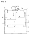
- Figure 1 is a sectional view showing an embodiment structure at gate electrode formation of the N-channel DMOSFET of the high withstand voltage DMOS portion in the BiCMOS process according to the present invention.
- an N+-type buried layer 2 is formed on a P-type semiconductor substrate 1.
- An N-type epitaxial layer 3 is grown over the buried layer 2, and then, a P+-type element isolation layer 4 which reaches the P-type semiconductor substrate 1 is formed to isolate an element island.
- a P-type well 5 and an N-type well 6 are formed in the isolated element island through ion-implantation processes for P- and N wells. In some cases, the P-type well 5 is not formed as described later.
- the N-type well 6 functions as an offset region as an expanded drain for reducing ON-resistance of the MOSFET.
- an active region is covered, for example, by a nitride film, and element-isolating insulative film (local oxidation film: LOGOS) 7 is formed on the P+-type isolation layer 4 and thick local oxidation film 7a is formed on the side of the P-type well 5 above the N-type well 6 by selectively oxidizing the nitride film.
- an ion-implanted layer 8 is formed by shallowly implanting impurities of the acceptor type (P-type) such as BF2 from the surface of the P-type well 5. As described later, the ion-implanted layer 8 is not formed in some cases.
- a gate electrode 10 is formed on gate insulation film 9 and the local oxidation film 7a.
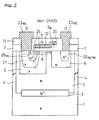
- Figure 2 is a sectional view showing an embodiment structure at source and drain electrode formation of the N-channel DMOSFET of the high withstand voltage DMOS portion in the BiCMOS process according to the present invention.
- a P-type base region (channel diffusion region) 21 is formed in the P-type well 5 more deeply than the diffusion depth of the ion-implanted layer 8 by employing a process for forming a P-type base of the bipolar transistor described later and by using the gate electrode 10 as a mask for self-alignment.
- side walls 25, 25, of, for example, oxide film deposited by the CVD technique, are formed on the side faces of the gate electrode 10 by an exclusive process or by employing a process for forming an LDD structure for the CMOS portion described later.
- an N+-type source region 26 NS is formed in the heavily doped P-type base region 21 by double diffusion using the gate electrode 10 and the side wall 25 as a mask for self-alignment, and at the same time, N+-type well-contact region (drain) 26 NCON is formed in the N-type well 6.
- inter-layer insulation film 12 contact holes are punched through the insulation film 12, and a source electrode 23 NS and a drain electrode 23 ND are formed. Then, a passivation film is deposited.
- the thick local oxidation film 7a relaxes electric field convergence onto the edge of the drain and contributes to increasing withstand voltage.
- N-channel type DMOS double diffused MOS
- DMOS double diffused MOS
- the DMOS structure usually facilitates reducing the P-type base resistance beneath the N+-type source region 26 NS
- a parasitic bipolar transistor comprised of the P-type base region 21 and the P-type well (drain region) 5 hardly operates, which prevents latching up and facilitates widening the safe operation area.
- the N+-type source region 26 NS is surrounded by the heavily doped P-type base region 21, punching through between the source and the drain is prevented, and withstand voltage increase is facilitated.
- the impurity concentration in the P-type base region 21 should be increased and its transverse diffusion length should be elongated for obtaining increased withstand voltage and current capacity. Since the P-type base region 21 is formed by employing the process for forming the P-type base region of the bipolar NPN transistor, the impurity concentration in the P-type base region of the NPN transistor exceeds the optimum concentration and the excess impurity concentration causes lowering of the current amplification factor h FE of the bipolar transistor.
- the present embodiment which prevents transverse diffusion of the N+-type source region from eroding too much the P-type base region by the side wall mask 25, rather facilitates lowering the impurity concentration in the P-type base region 21, by which increase of the current amplification factor h FE of the bipolar transistor is further facilitated.
- the present embodiment employs the process for forming the P-type base region of the bipolar transistor for forming the P-type base region 21, the process for forming the side walls of the LDD structure of the CMOS portion for forming the side wall 25, and the process for forming the N+-type source and drain of the CMOS portion for forming the N+-type source region 26 NS , respectively.
- a process for exclusively forming the N-type source may be inserted in advance to the formation process for the P-type base region 21 as the process sequence 2 of Table 1 describes. That is, as shown in Fig. 4, an N-type source region 26 NS ' is formed in the P-type well 5 by an exclusive process for forming the N-type source of the DMOS using the gate electrode 10 as a mask for self-alignment, and an N-type well-contact region 26 NCON ' in the N-type well 6. Then, the P-type base 21 is formed by employing the process for forming the P-type base region of the bipolar transistor using the gate electrode 10 as a mask for self-alignment. And, since the CMOS adopts the LDD structure, the contact holes are punched through the inter-layer insulation film 12 and the source electrode 23 NS and the drain electrode 23 ND are formed after the side walls 25, 25 are formed on the both side faces of the gate electrode 10.
- the impurity concentrations in the N-type source region 26 NS ' and the N-type well-contact region 26 NCON ' are lower than those in the N-type source region 26 NS and the N-type well-contact region 26 NCON shown in Fig. 2.
- the side wall 25 does not show a masking effect since the source region 26 NS ' is formed in advance to the side wall formation, the length of the P-type base region 21 in the total channel length can be set longer than that obtained by employing the CMOS process, since the impurity concentration in the N-type source region 26 NS ' can be controlled at the optimum value by the exclusive DMOS process. Therefore, the withstand voltage and the current capacity of the DMOS portion can be increased.
- the P-type base region is formed by employing the process for forming the P-type base region of the bipolar transistor in advance to the formation of the side wall 25, the DMOS structure which includes the N-type source region 26 NS ' and the P-type base region 21 in the P-type well 5 similarly as in the prior art can be obtained even when the side wall 25 is formed in the DMOS portion as well as in the CMOS portion. Therefore, the DMOS portion and the CMOS portion which include the side walls can be integrated into a monolithic circuit.
- the N-channel DMOSFET structure shown in Figs. 2 and 4 which is comprised of the P-type well 5 and the ion-implanted layer 8 may be replaced by an N-channel DMOSFET structure which lacks the P-type well and the ion-implanted layer as shown in Fig. 5.
- the DMOS portion of Fig. 5 is manufactured through the sequence 3 listed in Table 1.
- An N-type epitaxial layer 3 is grown over an N+-type buried layer 2 formed on a P-type semiconductor substrate 1, and then, an isolated element island is defined by forming a P+-type element isolation layer 4 which reaches the P-type semiconductor substrate 1. Then, only an N-type well 6 is formed in the isolated element island by ion-implantation and subsequent diffusion.
- the P-type well 5 is not formed.
- the N-type well 6 constitutes an offset region which functions as an expanded drain for decreasing ON-resistance of the MOSFET.
- element-isolating insulative film (local oxidation film: LOCOS) 7 is formed on the element isolation layer 4 and thick local oxidation film 7a on the edge side portion above the N-type well 6.
- a polysilicon gate electrode 10 is formed on gate insulation film 9 and the local oxidation film 7a.
- a P-type base region (channel diffusion region) 21 is formed by employing the base formation process of the bipolar transistor and by ion-implantation using the gate electrode 10 as a mask for self-alignment with respect to a broken line a-b in Fig. 5.
- a side wall 25 is formed on a side face of the gate electrode 10 by depositing oxide film by an exclusive process or by employing a CMOS process for forming an LDD structure described later, and by etching the oxide film by the anisotropic RIE technique.
- the width Lsw of the side wall is from 100 to 500 nm, which is controlled with accuracy of within 10 nm.
- an N+-type source region 26 NS is formed in the P-type base region 21 by employing a CMOS process for forming an N+-type source and a drain described later and by ion-implantation using the side wall 25 as a mask for self-alignment with respect to a broken line c-d in Fig. 5.
- an N+-type well-contact (drain) region 26 NCON is formed in the N-type well 6.
- the transverse diffusion length of the N+-type source region 26 NS and the side wall width Lsw should be selected so that the N+-type source region 26 NS may be positioned below the gate electrode 10.
- inter-layer insulation film 12 After forming inter-layer insulation film 12, contact holes are punched through the insulation film 12, and then, a source electrode 23 NS and a drain electrode 23 ND are formed. Then, a passivation film is formed.
- the thick local oxidation film 7a relaxes convergence of an electric field onto the drain edge and contributes to increasing withstand voltage. Since the thick local oxidation film 7a exists under the side wall on the drain side, the side wall does not affect to the formation of the N+-type drain region 26 NCON .
- the N+-type drain region 26 NCON is formed in a portion which is not covered by the thick local oxidation film 7a.
- Effective channel length Leff of the MOSFET is expressed by transverse diffusion length LPB of the P-type base region, transverse diffusion length LNS of the N+-type source region 26 NS , and the width Lsw of the side wall as follows.
- Leff LPB - LNS + Lsw (1) Since concentration gradient exists in the surface of the P-type base region 21, the acceptor amount in the offset portion introduced by the side wall formation occupies 80 % of the total acceptor amount.
- the effective channel length is extended to from 1 to 3 ⁇ m, if high temperature heat treatment is conducted for long period of time in forming the P-type base region 21.
- the DMOS structure of Fig. 5 reduces the channel resistance by from 58 to 86 % in comparison with the DMOS structure of Fig. 22.
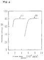
- Figure 6 shows the numerical simulation result on the relationship between dose amount in the P-type base and the breakdown voltage (withstand voltage of the device) for the DMOSFET (I) shown in Fig. 5 and the DMOSFET (II) the base region of which was not driven by high temperature heat treatment.
- the DMOSFETs (I) and (II) were manufactured through the similar process except the side wall formation for the DMOSFET (I). Though an excellent withstand voltage of 80 V is obtained by both DMOSFETs in the high dose amount region, withstand voltage decrease is caused by punching through between the source and the drain as the dose amount decreases.
- the dose amount for the DMOSFET (I) for obtaining the excellent withstand voltage of 80 V is one-third of that for the DMOSFET (II). That is, the crystal defects in the P-type base region is decreased by self-aligning the N+-type source region 26 NS using the side wall 25 as a mask.
- Figure 7 compares the surface concentration gradients of the DMOSFET (I) shown in Fig. 5 and the DMOSFET (II) shown in Fig. 22, the base region of which was not driven by high temperature heat treatment.
- threshold voltage dispersion caused by process parameter dispersion is reduced, since the maximum surface concentration is confined in the portion of small surface concentration gradient in the P-type base region 21 by forming the N+-type source region 26 NS using the side wall 25 as a mask for self-alignment.
- a DMOSFET structure shown in Fig. 8 does not include the ion-implanted layer 8, though it includes the P-type well as the DMOSFET structure of Fig. 2 does.
- the DMOS portion of Fig. 8 is manufactured through the sequence 4 of Table 1.
- An N-type epitaxial layer 3 is grown over an N+-type buried layer 2 formed on a P-type substrate 1, and then, an isolated element island is defined by forming a P+-type element isolation layer 4 which reaches the P-type semiconductor substrate 1.
- a P-type well 5 and an N-type well 6 are formed in the isolated element island by ion-implantation and subsequent thermal diffusion.
- the N-type well 6 constitutes an offset region which functions as an expanded drain for decreasing ON-resistance of the MOSFET. Then, after covering an active region with a nitride film and selectively oxidizing the nitride film, element-isolating insulative film (local oxidation film: LOCOS) 7 is formed on the element isolation layer 4 and thick local oxidation film 7a on the P-well side above the N-type well 6. A poly-silicon gate electrode 10 is formed on gate insulation film 9 and the local oxidation film 7a.
- LOCOS local oxidation film
- a P-type base region (channel diffusion region) 21 is formed by employing the base formation process of the bipolar transistor and by ion-implantation using the gate electrode 10 as a mask for self-alignment with respect to a broken line a-b in Fig. 8.
- a side wall 25 is formed on a side face of the gate electrode 10 by depositing oxide film by an exclusive process or by employing a CMOS process for forming an LDD structure described later, and by etching the oxide film by the anisotropic RIE technique.
- an N+-type source region 26 NS is formed in the P-type base region 21 by employing a CMOS process for forming an N+-type source and a drain described later and by ion-implantation using the side wall 25 as a mask for self-alignment with respect to a broken line c-d in Fig. 8.
- an N+-type well-contact region (drain) 26 NCON is formed in the N-type well 6.
- contact holes are punched through the insulation film 12, and then, a source electrode 23 NS and a drain electrode 23 ND are formed. Then, a passivation film is formed.
- This DMOSFET structure improves withstand voltage without so much deteriorating ON-resistance of the DMOSFET, since the P-type base region is diffused deeply and its surface concentration is relatively low.
- An N-channel DMOSFET structure shown in Fig. 9 includes an ion-implanted layer 8, though it does not include the P-type well.
- the DMOS portion of Fig. 9 is manufactured through the sequence 5 of Table 1.
- An N-type epitaxial layer 3 is grown over an N+-type buried layer 2 formed on a P-type semiconductor substrate 1, and then, an isolated element island is defined by forming a P+-type element isolation layer 4 which reaches the P-type semiconductor substrate 1.
- only an N-type well 6 is formed in the isolated element island by ion-implantation and subsequent thermal diffusion.
- the P-type well is not formed in this DMOSFET structure.
- the N-type well 6 constitutes an offset region which functions as an expanded drain for decreasing ON-resistance of the MOSFET. Then, after covering an active region with a nitride film and selectively oxidizing the nitride film, element-isolating insulative film (local oxidation film: LOCOS) 7 is formed on the element isolation layer 4 and thick local oxidation film 7a on the edge side portion above the N-type well 6. Then, in this embodiment, ion-implanted layer 8 is formed by implanting the acceptor (P-type) impurities such as BF2 shallowly by employing the CMOS process.
- P-type acceptor
- a polysilicon gate electrode 10 is formed on gate insulation film 9 and the local oxidation film 7a.
- a P-type base region (channel diffusion region) 21 is formed by employing the base formation process of the bipolar transistor and by ion-implantation using the gate electrode 10 as a mask for self-alignment with respect to a broken line a-b in Fig. 9.
- a side wall 25 is formed on a side face of the gate electrode 10 by depositing oxide film by an exclusive process or by employing a CMOS process for forming an LDD structure described later, and by etching the oxide film by the anisotropic RIE technique.
- an N+-type source region 26 NS is formed in the P-type base region 21 by employing a CMOS process for forming an N+-type source and a drain described later and by ion-implantation using the side wall 25 as a mask for self-alignment with respect to a broken line c-d in Fig. 8.
- an N+-type well-contact (drain) region 26 NCON is formed in the N-type well 6.
- contact holes are punched through the insulation film 12, and then, a source electrode 23 NS and a drain electrode 23 ND are formed. Finally, a passivation film is formed. This DMOSFET structure facilitates controlling the threshold voltage, since the process for forming the ion-implanted layer 8 exists.
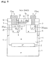
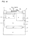
- Figure 10 is a sectional view showing an embodiment structure at gate electrode formation of the P-channel DMOSFET of the high withstand voltage DMOS portion in the BiCMOS process according to the present invention.
- the DMOS portion as described by the sequence 6 of Table 1, an N+-type buried layer 2 is formed on a P-type semiconductor substrate 1.
- An N-type epitaxial layer 3 is grown over the buried layer 2, and then, a P+-type element isolation layer 4 which reaches the P-type semiconductor substrate 1 is formed to isolate an element island.
- a P-type well 5 and an N-type well 6 are formed in the isolated element island by ion-implantation for P- and N wells and subsequent diffusion.
- the P-type well 5 functions as an offset region which functions as an expanded drain for reducing ON-resistance of the MOSFET.
- an active region is covered by a nitride film, and element-isolating insulative film (local oxidation film: LOCOS) 7 is formed on the P+-type isolation layer 4 and thick local oxidation film 7a is formed on the side of the N-type well above the P-type well 5 by selectively oxidizing the nitride film.
- an ion-implanted layer 8 is formed by shallowly implanting impurities of the acceptor type (P type) such as BF2 from the surface of the PS-type well 5.
- P type acceptor type
- a gate electrode 10 is formed on gate insulation film 9 and the local oxidation film 7a.
- Figure 11 is a sectional view showing an embodiment structure at source and drain electrode formation of the P-channel DMOSFET of the high withstand voltage DMOS portion in the BiCMOS process according to the present invention.
- a heavily doped P-type source region 22 PS is formed in the N-type well 6 by employing a process for forming a P-type base of the bipolar transistor using the gate electrode 10 as a mask for self-alignment.
- a P-type well-contact (drain) region 22 PCON is formed in the P-type well 5.
- side walls 25, 25 are formed on the side faces of the gate electrode 10 so as to conform with a process for forming an LDD structure adopted to the CMOS portion.
- an N+-type well-contact region 24 NCON is formed in the N-type well 6 by employing the process for forming the N+-type source and drain of the CMOS portion.
- contact holes are punched through the insulation film 12, and a source electrode 23 PS and a drain electrode 23 PD are formed.
- the thick local oxidation film 7a relaxes electric field convergence onto the drain edge and contributes to increasing withstand voltage.
- the DMOS structure comprised of the N-type well formed underneath the gate and the P-type source region 22 PS is obtained as by the prior art even when the side walls are formed in the DMOS portion as well as in the CMOS portion, since the P-type source region 22 PS and the P-type well-contact region (drain) 22 PCON are formed prior to the formation of the side wall 25. Therefore, the DMOS portion and the CMOS portion which includes the side walls can be integrated into a monolithic circuit.
- the P-type source region 22 PS and the P-type well-contact region 22 PCON of the P-channel DMOSFET transistor shown in Fig. 11 which are formed by employing the process for forming the P-type base region of the bipolar transistor may be replaced by a P-type source region 22 PS ' and a P-type well-contact region 22 PCON ' formed after the formation of the side wall 25 as shown in Fig. 12. That is, after the gate electrode 10 is formed, side walls 25 are formed, as described by the sequence 7 of Table 1, for the conformity with the CMOS process for forming the LDD structure.
- an N-type well-contact region 24 NCON ' is formed in the N-type well 6 by employing a CMOS process for forming an N+-type source and a drain.
- a P+-type source region 22 PS ' is formed by employing a CMOS process for forming its N+-type source and drain and by using the gate electrode 10 and the side wall 25 as a mask for self-alignment.
- a P+-type well-contact region 22 PCON ' is formed.
- contact holes are punched through the insulation film 12, and then, a source electrode 23 PS and a drain electrode 23 PD are formed.
- a DMOS structure is obtained which is comprised of the P+-type source region 22 PS ' and the N-type well 6.
- Transverse diffusion length of the heavily doped P+-type source region 22 PS ' of this DMOS structure is shorter by the side wall length (width) than that of the DMOS structure of Fig. 11, since the P+-type source region 22 PS ' is self-aligned by using the side wall 25 as a mask. Because of this, the DMOS structure of Fig. 12 facilitates suppressing withstand voltage decrease caused by surface punching through as well as increasing current capacity, since the total donor impurity amount in the surface layer of the N-type well underneath the gate electrode can be increased similarly as in the N-channel DMOS shown in Fig. 2.
- a P-channel region DMOS can be fabricated having a structure similar to that of the N-channel DMOS illustrated in Figure 5. That is, in place of the P-type base region 21 in Figure 5, an N-type base region is formed, and a P+-type source region is formed in place of N+-type source region 26 NS , a P-type well in place of N-type well 6, and a P+-type drain region in place of N+-type drain region 26 NCON .
- the N-type base region is formed using the gate electrode 10 as a mask for self-alignment
- the P+-type source region is formed using the side wall 25 as a mask for self-alignment.
- CMOS portion of the BiCMOS will be explained with reference to Figs. from 13 to 16.
- an N-type epitaxial layer 3 is grown over an N+-type buried layer 2 formed on a P-type semiconductor substrate 1, and then, an isolated element island is defined by forming a P+-type element isolation layer 4 which reaches the P-type semiconductor substrate 1.
- a P-type well 5 and an N-type well 6 are formed in the isolated element island by ion-implantation for P- and N wells and subsequent diffusion.
- a nitride film an active region is covered by a nitride film, and element-isolating insulative film (local oxidation film: LOCOS) 7 are formed on the P+-type isolation layer 4 and between the wells 5, 6 by selectively oxidizing the nitride film.
- ion-implanted layers 8, 8 are formed by shallowly implanting impurities of the acceptor type (P type) such as BF2 from the surface of the P-type well 5 and the N-type well 6.
- P type acceptor type
- gate electrodes 10, 10 are formed on gate insulation film 9 on the P-type well 5 and the N-type well 6.
- lightly doped N-type regions (LDD : lightly doped drain) 15, 15 are formed by implanting N-type impurities such as phosphorus using the gate electrode 10 on the P-type well 5 as a mask for self-alignment.
- N-type impurities such as phosphorus
- a P-type well-contact region 11 PCON is formed in the P-type well 5 by employing a process for forming a P-type base region of the bipolar transistor.
- a P-type source 11 PS and a P-type drain 11 PD are formed in the N-type well 6 by a self-alignment technique using the gate electrode 10 on the N-type well 6 as a mask.
- oxide film is deposited, for example by the CVD technique, and side walls 25 are formed on the side faces of the gate electrodes 10.
- an N-type source region 11 NS and an N-type drain region 11 ND are formed in the P-type well 5 by a self-alignment technique using the side wall 25 and the gate electrode 10 as a mask.
- N-type well-contact region 11 NCON is formed in the N-type well 6.
- the N-channel MOSFET of the DMOS portion in an LDD structure, an electric field in the drain is relaxed, hot carrier injection into the gate insulation film 9 is greatly suppressed, and reliability of the N-channel MOSFET is improved by preventing the gate insulation film 9 from deteriorating with elapse of time.
- a process for forming exclusively the P-type source and drain of the CMOS portion is eliminated from the above described processes for forming the LDD structure, which forms the P-type well-contact region 11 PCON in the P-type well 5 by employing the process for forming the P-type base region of the bipolar transistor and self-aligns the P-type source 11 PS and the P-type drain 11 PD in the N-type well 6 by using its gate electrode 10 as a mask.
- processing step decrease is realized even in constructing the LDD structure.
- the P-type well-contact region 11 PCON , the P-type source region 11 PS , and the P-type drain region 11 PD may be formed by employing the process for forming the P-type source and the drain of the CMOS portion as the sequence 9 of Table 1 describes. That is, as shown in Fig. 16, lightly doped N-type regions 15 are self-aligned by implanting N-type impurities such as phosphorus using the gate electrode 10 on the P-type well 5 as a mask, and then, side walls 25 are formed on the side faces of the gate electrodes 10. Then, an N+-type source 11 NS and an N+-type drain 11 ND are self-aligned in the P-type well 5 by using the side wall 25 and the gate electrode 10 as a mask.
- N+-type well-contact region 11 NCON is formed in the N-type well 6.
- a P+-type well-contact region 11 PCON , a P+-type source region 11 PS , and a P+-type drain region 11 PD are formed by employing the process for forming the P-type source and the drain of the CMOS portion. Even by the manufacturing method of the prior art, hot carrier injection into the gate insulation film 9 is greatly suppressed, and reliability of the N-channel MOSFET is improved.
- the bipolar transistor is comprised of a vertical NPN transistor and a transverse PNP transistor as shown in Fig. 17.
- an N-type epitaxial layer 3 is grown over anN+-type buried layer 2 formed on a P-type substrate 1, and then, an isolated element island is defined by forming a P+-type element isolation layer 4 which reaches the P-type semiconductor substrate 1.
- a P-type base region 31 PB is formed in the epitaxial layer 3.
- an N+-type emitter region 31NE and an N+-type collector region 32 NC are formed by employing the process for forming the N+-type source and the drain of the CMOS portion. Then, after forming inter-layer insulation film 12, contact holes are punched through the insulation film 12, and a base electrode 33 B , an emitter electrode 33 E and a collector electrode 33 C are formed.
- an N+-type base region 32 NB is formed by employing the process for forming the N+-type source and the drain of the CMOS portion, after forming in the epitaxial layer 3 a P-type emitter region 31 PE and a P-type collector region 31 PC by employing the process for forming the P-type base region 31 PB of the vertical transistor. Then, after forming the inter-layer insulation film 12, contact holes are punched through the insulation film 12, and a base electrode 34 B , an emitter electrode 34 E and a collector electrode 34 C are formed.
- the process for forming the N+-type source and the drain of the CMOS portion may be employed for forming the N+-type emitter region 32 NE and the N+-type collector region 32 NC of the NPN transistor as the sequence 12 of Table 1 describes.
- the process for forming the P-type base and drain of the CMOS portion can be employed for forming the P-type emitter region 31 PE and the P-type collector region 31 PC of the NPN transistor as described by the sequences 13 and 14 of Table 1.
- the process for forming the N-type source and drain of the DMOS portion can be employed for forming the N+-type base region (base-contact region) 32 NB of the PNP transistor as described by the sequence 15 of Table 1.
- the present invention is applicable also to the self-separation scheme which separates the elements by a P-type or an N-type semiconductor substrate.
- the present invention which forms a side wall on a side face of the gate electrode and utilizes the side wall as a mask for self-aligning the source region of the DMOS portion of the BiCMOS semiconductor apparatus for securing the transverse diffusion length difference in the DMOS portion, affords the following effects.
Landscapes
- Metal-Oxide And Bipolar Metal-Oxide Semiconductor Integrated Circuits (AREA)
Applications Claiming Priority (4)
| Application Number | Priority Date | Filing Date | Title |
|---|---|---|---|
| JP266761/93 | 1993-10-26 | ||
| JP26676193 | 1993-10-26 | ||
| JP110621/94 | 1994-05-25 | ||
| JP6110621A JPH07176640A (ja) | 1993-10-26 | 1994-05-25 | 半導体装置の製造方法 |
Publications (2)
| Publication Number | Publication Date |
|---|---|
| EP0653786A2 true EP0653786A2 (de) | 1995-05-17 |
| EP0653786A3 EP0653786A3 (de) | 1996-03-20 |
Family
ID=26450217
Family Applications (1)
| Application Number | Title | Priority Date | Filing Date |
|---|---|---|---|
| EP94116726A Withdrawn EP0653786A3 (de) | 1993-10-26 | 1994-10-24 | Verfahren zur Herstellung einer Halbleiteranordnung. |
Country Status (3)
| Country | Link |
|---|---|
| US (1) | US5591657A (de) |
| EP (1) | EP0653786A3 (de) |
| JP (1) | JPH07176640A (de) |
Cited By (8)
| Publication number | Priority date | Publication date | Assignee | Title |
|---|---|---|---|---|
| EP0682362A3 (de) * | 1994-05-13 | 1996-11-27 | Fuji Electric Co Ltd | Herstellungsverfahren für ein Halbleiterbauelement mit DMOS-Transistor. |
| EP0764988A3 (de) * | 1995-08-31 | 1998-03-04 | Texas Instruments Incorporated | Isolierter Leistungstransistor |
| US5739061A (en) * | 1993-10-26 | 1998-04-14 | Fuji Electric Co., Ltd. | Method of manufacturing a semiconductor device using gate side wall as mask for self-alignment |
| EP1271639A3 (de) * | 2001-06-29 | 2007-06-06 | ATMEL Germany GmbH | Verfahren zur Herstellung eines DMOS-Transistors |
| US7795691B2 (en) | 2008-01-25 | 2010-09-14 | Cree, Inc. | Semiconductor transistor with P type re-grown channel layer |
| EP2765612A4 (de) * | 2011-09-08 | 2015-07-22 | Tamura Seisakusho Kk | Ga2o3-halbleiterlement |
| US9461124B2 (en) | 2011-09-08 | 2016-10-04 | Tamura Corporation | Ga2O3 semiconductor element |
| CN114038758A (zh) * | 2022-01-07 | 2022-02-11 | 广州粤芯半导体技术有限公司 | 改善热载流子注入的nmos的形成方法 |
Families Citing this family (22)
| Publication number | Priority date | Publication date | Assignee | Title |
|---|---|---|---|---|
| US6303961B1 (en) | 1998-04-29 | 2001-10-16 | Aqere Systems Guardian Corp. | Complementary semiconductor devices |
| GB2374456A (en) | 2000-12-09 | 2002-10-16 | Esm Ltd | High-voltage metal oxide semiconductor device and method of forming the device |
| US6825543B2 (en) * | 2000-12-28 | 2004-11-30 | Canon Kabushiki Kaisha | Semiconductor device, method for manufacturing the same, and liquid jet apparatus |
| US20020130361A1 (en) * | 2001-03-16 | 2002-09-19 | Semiconductor Components Industries, Llc | Semiconductor device with laterally varying p-top layers |
| JP5151258B2 (ja) * | 2006-06-15 | 2013-02-27 | 株式会社リコー | 昇圧型dc−dcコンバータ用の半導体装置及び昇圧型dc−dcコンバータ |
| US7723785B2 (en) * | 2007-07-31 | 2010-05-25 | Taiwan Semiconductor Manufacturing Company, Ltd. | High performance power MOS structure |
| KR101405310B1 (ko) * | 2007-09-28 | 2014-06-12 | 삼성전자 주식회사 | 반도체 집적 회로 장치 및 그 제조 방법 |
| US20090090981A1 (en) * | 2007-10-05 | 2009-04-09 | Kazuhiro Natsuaki | Semiconductor device |
| US7915128B2 (en) * | 2008-02-29 | 2011-03-29 | Taiwan Semiconductor Manufacturing Company, Ltd. | High voltage semiconductor devices |
| JP5354951B2 (ja) * | 2008-05-13 | 2013-11-27 | ラピスセミコンダクタ株式会社 | 半導体装置及びその製造方法 |
| JP5359107B2 (ja) * | 2008-08-11 | 2013-12-04 | ミツミ電機株式会社 | 半導体装置及びその製造方法 |
| JP2010118622A (ja) | 2008-11-14 | 2010-05-27 | Panasonic Corp | 半導体装置及びその製造方法 |
| US9184097B2 (en) * | 2009-03-12 | 2015-11-10 | System General Corporation | Semiconductor devices and formation methods thereof |
| KR101098447B1 (ko) | 2009-12-04 | 2011-12-26 | 매그나칩 반도체 유한회사 | 반도체 장치 |
| KR101175228B1 (ko) * | 2009-12-04 | 2012-08-21 | 매그나칩 반도체 유한회사 | 반도체 장치 |
| US9076837B2 (en) * | 2012-07-06 | 2015-07-07 | Taiwan Semiconductor Manufacturing Company, Ltd. | Lateral insulated gate bipolar transistor structure with low parasitic BJT gain and stable threshold voltage |
| JP6064240B2 (ja) * | 2012-08-17 | 2017-01-25 | ローム株式会社 | 半導体装置および半導体装置の製造方法 |
| US9917168B2 (en) | 2013-06-27 | 2018-03-13 | Taiwan Semiconductor Manufacturing Company, Ltd. | Metal oxide semiconductor field effect transistor having variable thickness gate dielectric |
| CN104701372B (zh) * | 2013-12-06 | 2017-10-27 | 无锡华润上华科技有限公司 | 横向扩散金属氧化物半导体器件及其制造方法 |
| JP7148440B2 (ja) | 2019-03-06 | 2022-10-05 | 株式会社東芝 | 半導体装置 |
| US11430866B2 (en) * | 2020-03-26 | 2022-08-30 | Intel Corporation | Device contact sizing in integrated circuit structures |
| JP7398339B2 (ja) * | 2020-05-29 | 2023-12-14 | ルネサスエレクトロニクス株式会社 | 半導体装置 |
Family Cites Families (10)
| Publication number | Priority date | Publication date | Assignee | Title |
|---|---|---|---|---|
| US4104784A (en) * | 1976-06-21 | 1978-08-08 | National Semiconductor Corporation | Manufacturing a low voltage n-channel MOSFET device |
| US4217688A (en) * | 1978-06-12 | 1980-08-19 | Rca Corporation | Fabrication of an integrated injection logic device incorporating an MOS/bipolar current injector |
| US4503598A (en) * | 1982-05-20 | 1985-03-12 | Fairchild Camera & Instrument Corporation | Method of fabricating power MOSFET structure utilizing self-aligned diffusion and etching techniques |
| US4716126A (en) * | 1986-06-05 | 1987-12-29 | Siliconix Incorporated | Fabrication of double diffused metal oxide semiconductor transistor |
| ATE93654T1 (de) * | 1988-04-22 | 1993-09-15 | Asea Brown Boveri | Abschaltbares leistungshalbleiterbauelement. |
| US5072267A (en) * | 1989-06-28 | 1991-12-10 | Nec Corporation | Complementary field effect transistor |
| JP2525257B2 (ja) * | 1989-11-16 | 1996-08-14 | セイコー電子工業株式会社 | 半導体集積回路装置の製造方法 |
| JPH03244135A (ja) * | 1990-02-22 | 1991-10-30 | New Japan Radio Co Ltd | Mosトランジスタの製造方法 |
| US5171699A (en) * | 1990-10-03 | 1992-12-15 | Texas Instruments Incorporated | Vertical DMOS transistor structure built in an N-well CMOS-based BiCMOS process and method of fabrication |
| JP3196313B2 (ja) * | 1991-09-05 | 2001-08-06 | 富士電機株式会社 | 半導体装置の製造方法 |
-
1994
- 1994-05-25 JP JP6110621A patent/JPH07176640A/ja active Pending
- 1994-10-24 EP EP94116726A patent/EP0653786A3/de not_active Withdrawn
- 1994-10-26 US US08/329,943 patent/US5591657A/en not_active Expired - Fee Related
Cited By (11)
| Publication number | Priority date | Publication date | Assignee | Title |
|---|---|---|---|---|
| US5739061A (en) * | 1993-10-26 | 1998-04-14 | Fuji Electric Co., Ltd. | Method of manufacturing a semiconductor device using gate side wall as mask for self-alignment |
| EP0682362A3 (de) * | 1994-05-13 | 1996-11-27 | Fuji Electric Co Ltd | Herstellungsverfahren für ein Halbleiterbauelement mit DMOS-Transistor. |
| EP0764988A3 (de) * | 1995-08-31 | 1998-03-04 | Texas Instruments Incorporated | Isolierter Leistungstransistor |
| EP1271639A3 (de) * | 2001-06-29 | 2007-06-06 | ATMEL Germany GmbH | Verfahren zur Herstellung eines DMOS-Transistors |
| US7795691B2 (en) | 2008-01-25 | 2010-09-14 | Cree, Inc. | Semiconductor transistor with P type re-grown channel layer |
| EP2765612A4 (de) * | 2011-09-08 | 2015-07-22 | Tamura Seisakusho Kk | Ga2o3-halbleiterlement |
| US9437689B2 (en) | 2011-09-08 | 2016-09-06 | Tamura Corporation | Ga2O3 semiconductor element |
| US9461124B2 (en) | 2011-09-08 | 2016-10-04 | Tamura Corporation | Ga2O3 semiconductor element |
| US10249767B2 (en) | 2011-09-08 | 2019-04-02 | Tamura Corporation | Ga2O3-based semiconductor element |
| CN114038758A (zh) * | 2022-01-07 | 2022-02-11 | 广州粤芯半导体技术有限公司 | 改善热载流子注入的nmos的形成方法 |
| CN114038758B (zh) * | 2022-01-07 | 2022-04-15 | 广州粤芯半导体技术有限公司 | 改善热载流子注入的nmos的形成方法 |
Also Published As
| Publication number | Publication date |
|---|---|
| JPH07176640A (ja) | 1995-07-14 |
| US5591657A (en) | 1997-01-07 |
| EP0653786A3 (de) | 1996-03-20 |
Similar Documents
| Publication | Publication Date | Title |
|---|---|---|
| US5591657A (en) | Semiconductor apparatus manufacturing method employing gate side wall self-aligning for masking | |
| US5171699A (en) | Vertical DMOS transistor structure built in an N-well CMOS-based BiCMOS process and method of fabrication | |
| KR101145558B1 (ko) | 비대칭 헤테로―도핑된 고―전압mosfet(ah2mos) | |
| US7602024B2 (en) | Modular bipolar-CMOS-DMOS analog integrated circuit and power transistor technology | |
| EP1193767B1 (de) | Bipolartransistor mit isoliertem Gate | |
| US7187033B2 (en) | Drain-extended MOS transistors with diode clamp and methods for making the same | |
| US5465000A (en) | Threshold adjustment in vertical DMOS devices | |
| EP0731504B1 (de) | Verfahren zur Herstellung von intergrierten Schaltungen mit Hochspannungs- und Niederspannungs-lateralen-DMOS-Leistungsbauelementen und nichtflüchtigen Speicherzellen | |
| KR20130103640A (ko) | 절연 트랜지스터 및 다이오드 | |
| EP0682362B1 (de) | Herstellungsverfahren für ein Halbleiterbauelement mit DMOS-Transistor | |
| JPH06318697A (ja) | Dmos構造及びその製造方法 | |
| US5739061A (en) | Method of manufacturing a semiconductor device using gate side wall as mask for self-alignment | |
| US20120299114A1 (en) | Semiconductor device and method of manufacturing the same | |
| KR100425230B1 (ko) | 반도체 장치와 그 제조 방법 | |
| US6153473A (en) | Method of symmetrically implanted punch-through stopper for a rugged DMOS power device | |
| US20070200171A1 (en) | Seminconductor device and method of manufacturing the same | |
| GB2561388B (en) | Silicon carbide integrated circuit | |
| JP4800566B2 (ja) | 半導体装置及びその製造方法 | |
| US6297119B1 (en) | Semiconductor device and its manufacture | |
| JPH09134965A (ja) | 半導体装置及びその製造方法 | |
| CN101589471A (zh) | 半导体器件及形成半导体器件的方法 | |
| JP3300238B2 (ja) | 半導体装置及びその製造方法 |
Legal Events
| Date | Code | Title | Description |
|---|---|---|---|
| PUAI | Public reference made under article 153(3) epc to a published international application that has entered the european phase |
Free format text: ORIGINAL CODE: 0009012 |
|
| AK | Designated contracting states |
Kind code of ref document: A2 Designated state(s): DE FR NL |
|
| PUAL | Search report despatched |
Free format text: ORIGINAL CODE: 0009013 |
|
| AK | Designated contracting states |
Kind code of ref document: A3 Designated state(s): DE FR NL |
|
| RHK1 | Main classification (correction) |
Ipc: H01L 21/8249 |
|
| STAA | Information on the status of an ep patent application or granted ep patent |
Free format text: STATUS: THE APPLICATION IS DEEMED TO BE WITHDRAWN |
|
| 18D | Application deemed to be withdrawn |
Effective date: 19960921 |