EP0653850A2 - Circuit pour reconnaître l'interférence d'un canal adjacent - Google Patents
Circuit pour reconnaître l'interférence d'un canal adjacent Download PDFInfo
- Publication number
- EP0653850A2 EP0653850A2 EP94116879A EP94116879A EP0653850A2 EP 0653850 A2 EP0653850 A2 EP 0653850A2 EP 94116879 A EP94116879 A EP 94116879A EP 94116879 A EP94116879 A EP 94116879A EP 0653850 A2 EP0653850 A2 EP 0653850A2
- Authority
- EP
- European Patent Office
- Prior art keywords
- signal
- channel interference
- circuit arrangement
- adjacent channel
- arrangement according
- Prior art date
- Legal status (The legal status is an assumption and is not a legal conclusion. Google has not performed a legal analysis and makes no representation as to the accuracy of the status listed.)
- Granted
Links
Images



Classifications
-
- H—ELECTRICITY
- H04—ELECTRIC COMMUNICATION TECHNIQUE
- H04B—TRANSMISSION
- H04B1/00—Details of transmission systems, not covered by a single one of groups H04B3/00 - H04B13/00; Details of transmission systems not characterised by the medium used for transmission
- H04B1/06—Receivers
- H04B1/16—Circuits
- H04B1/1646—Circuits adapted for the reception of stereophonic signals
- H04B1/1661—Reduction of noise by manipulation of the baseband composite stereophonic signal or the decoded left and right channels
-
- H—ELECTRICITY
- H04—ELECTRIC COMMUNICATION TECHNIQUE
- H04B—TRANSMISSION
- H04B1/00—Details of transmission systems, not covered by a single one of groups H04B3/00 - H04B13/00; Details of transmission systems not characterised by the medium used for transmission
- H04B1/06—Receivers
- H04B1/10—Means associated with receiver for limiting or suppressing noise or interference
- H04B1/1027—Means associated with receiver for limiting or suppressing noise or interference assessing signal quality or detecting noise/interference for the received signal
-
- Y—GENERAL TAGGING OF NEW TECHNOLOGICAL DEVELOPMENTS; GENERAL TAGGING OF CROSS-SECTIONAL TECHNOLOGIES SPANNING OVER SEVERAL SECTIONS OF THE IPC; TECHNICAL SUBJECTS COVERED BY FORMER USPC CROSS-REFERENCE ART COLLECTIONS [XRACs] AND DIGESTS
- Y10—TECHNICAL SUBJECTS COVERED BY FORMER USPC
- Y10S—TECHNICAL SUBJECTS COVERED BY FORMER USPC CROSS-REFERENCE ART COLLECTIONS [XRACs] AND DIGESTS
- Y10S977/00—Nanotechnology
- Y10S977/84—Manufacture, treatment, or detection of nanostructure
- Y10S977/849—Manufacture, treatment, or detection of nanostructure with scanning probe
- Y10S977/86—Scanning probe structure
- Y10S977/872—Positioner
Definitions
- the invention relates to a circuit arrangement for the detection of adjacent channel interference in a stereo broadcast receiver in which a stereo multiplex signal is present. Furthermore, the invention is concerned with measures for reducing the subjectively perceived interference effect of adjacent channel interference.
- the object of the present invention is therefore to detect such faults, which should preferably be implemented using digital circuits, preferably using integrated circuit technology. It is also intended within the scope of the invention to reduce the subjective interference effect of adjacent channel interference.
- the detection of adjacent channel interference is effected in the circuit arrangement according to the invention in that, depending on a DC voltage component and in Depending on spectral components above 60 kHz, a signal indicating the adjacent channel interference (adjacent channel interference signal) is derived.
- adjacent channel interference By using two criteria for recognizing adjacent channel interference, a distinction can be made between adjacent channel interference and other types of interference in the circuit arrangement according to the invention, which also lead to higher-frequency spectral components in the stereo multiplex signal.
- interference is, for example, multi-path reception or ignition interference.
- a first auxiliary signal is derived when the direct voltage component of the stereo multiplex signal is greater than a first reference value
- a second auxiliary signal is formed when the amplitudes of the spectral components above 60 kHz of the stereo Multiplex signals are greater than a second reference value
- Advantageous embodiments of the circuit arrangement according to the invention consist in that the first auxiliary signal is derived in that the stereo multiplex signal is low-pass filtered and rectified and in that the rectified signal is compared with the first reference value and that the high-pass filtered Stereo multiplex signal is rectified and low-pass filtered and that the low-pass filtered signal is compared with the second reference value.
- a reduction in the subjectively perceived interference effect with the aid of the adjacent channel interference signal can result from an attenuation of the audio signals by, for example, 10 dB to 20 dB.
- a particularly advantageous way of reducing the interference effect is, however, that the adjacent channel interference signal can be fed to an integrator which integrates in one direction in the presence of adjacent channel interference and in the opposite direction in the absence of adjacent channel interference, and in that the output signal of the integrator attenuates from the stereo multiplex signal obtained audio signals in such a way that when integrated in the opposite direction, the attenuation increases.
- the duration of adjacent channel interference is taken into account in an advantageous manner. It is advantageous if the time constant of the integrator in one direction is less than in the opposite direction or equal to zero. In order to avoid excessive damping, it can be provided that the output signal of the integrator is passed through a limiter.
- circuit arrangement according to the invention consists in that when further signals representing the reception quality are derived, the adjacent channel interference signal is superimposed on these signals and that the signal which is produced as a result is subsequently limited.
- circuit arrangement according to the invention can be implemented in various ways. For example, individual or groups of the blocks shown can be implemented using suitable circuits, in particular integrated circuits. With a very high degree of integration, it is also possible to implement the entire digital signal processing of the receiver in an integrated circuit, signal processing steps, such as filtering or nonlinear weighting, being carried out by arithmetic operations.
- An integrated circuit can be used to implement a receiver
- digital signal processors and other digital circuits such as shift registers, flip-flops etc., can be arranged together.
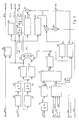
- a stereo multiplex signal MPX is supplied, which has a sampling rate of 228 kHz, which has proven to be advantageous in the previous digital signal processing. Since a substantially lower sampling rate is sufficient to form the first auxiliary signal SKU, the stereo multiplex signal MPX is passed via a low-pass filter 2 to a circuit 3 for reducing the sampling rate around the divider 24.
- the resulting signal is fed to a further low-pass filter 4, the cut-off frequency of which is very low, so that at its output there is practically only the DC voltage component of which the amount is formed at 5.
- This is compared in a comparator 6 with a constant C1 supplied at 7 of, for example, 0.07 (based on the maximum amplitude). If the amount of the DC voltage component is smaller than the constant C1, a 1 appears at the output x ⁇ y of the comparator 6, which is fed to an input of an AND circuit 8.
- a signal FST is fed to a further input 9 of the circuit arrangement according to FIG. 1, which corresponds to the field strength of the respectively received signal.
- This signal is low-pass filtered at 10 and compared to a constant C2 at 11. If the field strength is greater than a value specified by the constant C2, a 1 appears at the output x ⁇ y of the comparator 11, which also corresponds to the AND circuit 8 is directed. If both conditions are met, the stop signal SLS at the output 12 of the AND circuit 8 also assumes level 1.
- auxiliary signal SKU To derive the auxiliary signal SKU, a further comparator 13 is supplied, to which a constant C3 is supplied as a reference value. If the DC voltage component supplied by the magnitude generator 5 is greater than or equal to C3, the first auxiliary signal SKU assumes level 1 at the output 14.
- Fig. 2 shows the processing of a multiplex signal MPX1 up to audio signals for four channels.
- a digital stereo multiplex signal MPX1 is fed to an input 43 from an FM demodulator, while a further input 44 receives the signal AM1 from an AM demodulator.
- the sampling rate of the MPX1 signal is 456 kHz, which is an integer multiple of the carrier frequency of the radio data signal (57 kHz).
- this high sampling frequency requires a large number of arithmetic operations per second.
- the aim is therefore to work with the lowest possible sampling rates which are adapted to the bandwidth of the respective signal.
- the signal MPX1 is therefore subjected to a sampling rate halving at 45, for which purpose a low-pass filtering 46 is required beforehand.
- a low-pass filter 46 since the low-pass filter required per se, with a rectilinear frequency response over most of the pass band and a steep drop in the half-sampling frequency range, is very expensive, a low-pass filter 46 has been used which has a gradual drop.
- a compensation filter 47 with an opposite frequency response cancels the error that arises as a result.
- the signal MPX2 with a sampling frequency of 228 kHz is fed to a circuit 48 for automatic interference suppression. Such circuits suppress short pulse-shaped interference and have become known under the abbreviation ASU.
- the output signal MPX3 of the circuit 48 goes into a stereo decoder 49, which generates the two audio signals L1 and R1 (left and right), which are subjected to a sampling rate conversion around the divider 5 at 50.
- the resulting audio signals L2, R2 are fed via a circuit 51 with controllable damping as signals LFM and RFM inputs to a source switch 52. In a manner not shown, other audio signals can be fed to the source switch, for example from a CD player or a tape device.
- the output signals of the source switch 52 arrive as signals L, R at an audio processor 53, with the aid of which settings, such as volume, fader, balance and raising and lowering or raising, are carried out.
- the audio processor 53 has four outputs 54, 55, 56, 57, of which the signals LF, LR, RF and RR can each be fed to an output stage (not shown) for four loudspeakers.
- the stereo multiplex signal MPX2 also reaches a decoder 58 for traffic radio signals and / or radio data signals.
- the signal MPX2 is also required by a circuit 59 for the search stop and the first auxiliary signal SKU. An embodiment of this circuit has been described in connection with FIG. 1.
- a control unit 60 receives signals from the circuits 58, 59 and 42 and from the stereo decoder 49. It outputs signals to the circuit 42, the source switch 52 and the audio processor 53. Further connections of the control unit 60 - For example, with control and display devices - are not shown in Fig. 2.
- a signal is required which consists of the parts of the stereo multiplex signal above 60 kHz. This is generated in the circuit 41, to which the signals MPX1 and MPX2 are supplied.
- An exemplary embodiment of the circuit 41 is explained in more detail in patent application P 43 09 518.6 together with other details of the block diagrams according to FIGS. 2 and 3.
- FIG 3 illustrates details of circuit 42 ( Figure 2) used to derive signals describing the quality of the signals received.
- the output signal AM1 of an amplitude demodulator not shown, is supplied. It serves as a measure of the field strength.
- the signal AM1 with a sampling frequency of 456 kHz is first subjected to low-pass filtering in a filter 62. Together with the comb filter 65, this prevents that in the subsequent subsampling by a factor of 2 at 63 and later by a factor of 24 at 64, higher-frequency spectral components map to the direct component and falsify it in an impermissible manner.
- Another low-pass filtering (comb filter) 65 is provided between the scanning elements 63 and 64.
- the field strength signal thus decimated with respect to the sampling rates is averaged in two low-pass elements 66, 67 with different time constants.
- a switch 68 forwards one of the output signals of the low-pass elements 66, 67 as the signal AMC. This is weighted at 69 in the form of a noise curve to generate the noise attenuation A FE .
- the field strength signal of the smaller time constant, ie the "fast" field strength signal FST16 at the output of the Low-pass element 66 also serves to reduce the stereo channel separation D when the field strength drops.
- the further processing of the signals A FE and FST16 is explained in the patent application P 43 09 518.6 by the applicant.
- a high-pass detector 70, a symmetry detector 71 and a logic network 72 are used to generate the further signal DD2, the output signal DD1 of which is passed via a pulse width discriminator 73.
- the high-pass detector 70 which is explained in detail in FIG. 4, is supplied with an MPX5 signal via an input 74 and a sampling rate reduction 75, which contains portions of the stereo multiplex signal above 60 kHz, but which is already in the baseband are transformed.
- the second auxiliary signal BHD is set to level 1 in the high-pass detector 70 if spectral components above 60 kHz are present.
- This second auxiliary signal BHD together with the first auxiliary signal SKU supplied at 95, is fed to a non-AND circuit 96, which forms the adjacent channel interference signal DD3, which assumes the level, 0 in the event of adjacent channel interference.
- This signal is fed to an input of an integrator 81.
- Another output signal AHD of the high-pass detector 70 assumes the value 1 if the amplitude of signal components above 60 kHz is above a threshold value. This has the fundamental advantage of being able to react very punctually to any type of malfunction - including those that are not multi-way malfunctions. In extreme cases, however, it can lead to a fault being reported, but which does not yet lead to any audible disturbances in the receiver's external NF signal. In this case, however, the measures envisaged for masking faults would still occur be initiated.
- the symmetry of the carrier-frequency stereo difference signal is evaluated to detect audible interference that is not an adjacent channel interference. It is important in this procedure, on the one hand, that an undisturbed signal must be symmetrical to the carrier due to the two-sideband amplitude modulation, and, on the other hand, that the useful signal is considered directly here. An asymmetry therefore leads to the conclusion that there is an interference that can also be heard in the LF signal.
- Signals are fed to the symmetry detector 71 via inputs 76 to 79 from a stereo decoder (FIG. 2), which essentially represent the product of the carrier-frequency stereo difference signal with a reference carrier which is in quadrature with the subcarrier.
- the output signal ASD of the symmetry detector assumes the value 1 if there is asymmetry.
- the use of one of the signals AHD or ASD as a further signal DD2 already brings considerable advantages.
- both detectors 70, 71 are provided, the output signals AHD and ASD being routed via a logic network 72.
- this has the advantage that in the case of pure mono broadcasts in which no carrier-frequency stereo difference signal is transmitted, the further auxiliary signal DD2 is derived by the high-pass detector 70.
- the derivation of the further signal DD2 is also possible with methods for stereo signal transmission which deviate from the European standard - for example with the FMX method in the USA.
- the logical network enables the selection or the type of logical combination of the two signals AHD and ASD to signal DD1.
- the signal DD1 is over a Pulse width discriminator 73 passed, which ensures that the output signal DD2 only indicates a fault when the input signal DD1 is active for an adjustable minimum period.
- the signal DD2 switches between a large and a small time constant when the field strength signal is formed.
- the signal DD2 also serves as a trigger signal for two asymmetrical integrators 80, 81, of which an exemplary embodiment is shown in FIG. 5.
- the output signals AT1 and AMU of the asymmetrical integrators 80, 81 jump to 0 at the moment of triggering or to a preset value between 0 and 1 and remain at these values as long as DD2 and DD3 are at zero, in order to then linearly increase with adjustable time constants to increase a maximum value.
- the signal AT1 is fed to a multiplier 83 together with the field strength signal WF2 weighted at 82. This forms a signal that masks interference in the LF signal by reducing the stereo channel separation. This is multiplied in a further multiplier 84 by a signal FMO supplied at 85, which is used to forcibly cancel the stereo channel separation.
- Signal D can be taken from output 86 and fed to the stereo decoder.
- the output signal AMU of the asymmetrical integrator 81 is fed together with the signal A FE to a further multiplier 87, which, after limitation at 97 and sampling rate conversion at 98 and 99, produces a signal AFE_AMU which attenuates the LF signal by a maximum of that caused by the limiter 97 causes predetermined value that can be taken from the output 88.
- the circuit arrangement according to FIG. 3 has three further outputs 89, 90, 91, at which signals can be removed which describe the field strength.
- the FST16 signal is 16 bit accurate. For some purposes, however, a signal with lower accuracy is also sufficient, which is why a field strength signal FST8 with a bit width of 8 is generated with the aid of a compression characteristic curve 92.
- the signals FST16 and FST8 are fast enough for the purpose of identifying the signal quality, but they are not free from a certain inertia due to the filters described in connection with FIG. 3 and possibly due to the amplitude demodulation.
- a signal VFST can be fed in via an input 93 from a microcontroller (not shown).
- a signal DFST is generated from this signal and the signal FST16 with the aid of a comparator 94, the respective level (0 or 1) of which depends on whether the signal VFST or the signal FST16 is larger.
- the signal DFST which can be taken off at output 89 indicates the direction of change of the field strength.
- the high-pass detector 70 is explained in more detail below with reference to FIG. 4.
- the signal MPX5 can be fed to an input 100 of the high-pass detector in accordance with FIG. If the averaged signal exceeds a threshold HDS, the output signal of a comparator consisting of a subtractor 103 and a sign recognition 104, 105 assumes the value 1.
- the signal AHD at the output 106 also assumes the value 1 if the sign of the output signal of the subtractor 103 is positive.
- Another comparator is formed by a further subtractor 107 and a further sign recognition 108, 109.
- the second auxiliary signal BHD at output 110 assumes the value 1 if the higher-frequency spectral components exceed the reference value HDT.
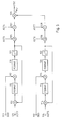
- FIG. 5 An embodiment of the asymmetrical integrator 81 (FIG. 3) is shown in FIG. 5.
- Two integrators are provided per se, to which the signals DD2 and DD3 can be fed via inputs 111 and 112.
- Each integrator consists of an adder 113, 114, two format converters 115, 116 and 119, 120, a multiplier 117, 118 and a delay 121, 122 by one sampling period.
- AST2 and AST5 are applied.
- the signal DD3 changes to the value 0. This has the consequence that the integrator for the adjacent channel interference signal DD3 is set to 0.
- DD3 At the end of an adjacent channel disturbance, DD3 returns to level 1, whereupon the integrator starts up to the value 1 by integrating the constants AST5.
- the procedure for signal DD2 is similar.
- the output signals of both integrators are evaluated at 125, 126 with a constant AST3, AST6 and then added at 127, 128 to a further constant AST4, AST7.
- the results are multiplied together at 129 and can be taken from an output 130 as signal A MU .
Landscapes
- Engineering & Computer Science (AREA)
- Computer Networks & Wireless Communication (AREA)
- Signal Processing (AREA)
- Stereo-Broadcasting Methods (AREA)
- Noise Elimination (AREA)
- Monitoring And Testing Of Transmission In General (AREA)
- Stereophonic System (AREA)
- Time-Division Multiplex Systems (AREA)
Applications Claiming Priority (2)
| Application Number | Priority Date | Filing Date | Title |
|---|---|---|---|
| DE4338700 | 1993-11-12 | ||
| DE4338700A DE4338700C2 (de) | 1993-11-12 | 1993-11-12 | Schaltungsanordnung zum Erkennen von Nachbarkanalstörungen in einem Stereo-Multiplex-Rundfunkempfänger |
Publications (3)
| Publication Number | Publication Date |
|---|---|
| EP0653850A2 true EP0653850A2 (fr) | 1995-05-17 |
| EP0653850A3 EP0653850A3 (fr) | 1995-11-29 |
| EP0653850B1 EP0653850B1 (fr) | 2002-02-27 |
Family
ID=6502466
Family Applications (1)
| Application Number | Title | Priority Date | Filing Date |
|---|---|---|---|
| EP94116879A Expired - Lifetime EP0653850B1 (fr) | 1993-11-12 | 1994-10-26 | Circuit pour reconnaítre l'interférence d'un canal adjacent |
Country Status (6)
| Country | Link |
|---|---|
| US (1) | US5631963A (fr) |
| EP (1) | EP0653850B1 (fr) |
| JP (1) | JPH07193553A (fr) |
| AT (1) | ATE213883T1 (fr) |
| DE (2) | DE4338700C2 (fr) |
| ES (1) | ES2173104T3 (fr) |
Cited By (2)
| Publication number | Priority date | Publication date | Assignee | Title |
|---|---|---|---|---|
| WO1997023959A3 (fr) * | 1995-12-22 | 1997-09-12 | Philips Electronics Nv | Recepteur et dispositif de detection des interferences entre canaux voisins |
| DE102012201372A1 (de) * | 2012-01-31 | 2013-08-01 | Sennheiser Electronic Gmbh & Co. Kg | Stationärer, analoger FM-Empfänger zum Empfangen von analogen, drahtlos übertragenen FM-Audiosignalen von mindestens einer mobilen Einheit und Verfahren zum Empfangen eines analogen, frequenzmodulierten Audiosignals von einem mobilen analogen FM-Sender |
Families Citing this family (6)
| Publication number | Priority date | Publication date | Assignee | Title |
|---|---|---|---|---|
| DE4434451A1 (de) * | 1994-09-27 | 1996-03-28 | Blaupunkt Werke Gmbh | Amplitudendemodulator |
| US6453251B1 (en) * | 1999-10-07 | 2002-09-17 | Receptec Llc | Testing method for components with reception capabilities |
| US7127008B2 (en) | 2003-02-24 | 2006-10-24 | Ibiquity Digital Corporation | Coherent AM demodulator using a weighted LSB/USB sum for interference mitigation |
| JP4133604B2 (ja) * | 2003-06-10 | 2008-08-13 | アルパイン株式会社 | ラジオ受信機 |
| DE602006011422D1 (fr) | 2006-02-15 | 2010-02-11 | Sony Deutschland Gmbh | |
| ATE527759T1 (de) * | 2009-05-11 | 2011-10-15 | Harman Becker Automotive Sys | Signalanalyse zur verbesserten erkennung von geräuschen aus einem benachbarten kanal |
Family Cites Families (6)
| Publication number | Priority date | Publication date | Assignee | Title |
|---|---|---|---|---|
| JPS5843301Y2 (ja) * | 1977-07-02 | 1983-09-30 | ヤマハ株式会社 | 受信機における受信状態自動選択回路 |
| US5204904A (en) * | 1986-12-01 | 1993-04-20 | Carver Corporation | Apparatus for receiving and processing frequency modulated electromagnetic signals |
| DE3721918C1 (en) * | 1987-07-02 | 1988-11-24 | Becker Autoradio | Method for evaluating the suitability for reception of the frequency-modulated broadcast transmissions received in an FM broadcast receiver, and circuit arrangement for carrying out the method |
| US5201062A (en) * | 1990-03-28 | 1993-04-06 | Pioneer Electronic Corporation | Noise reducing circuit |
| DE4309518A1 (de) * | 1993-03-24 | 1994-10-06 | Blaupunkt Werke Gmbh | Schaltungsanordnung zur Ableitung mindestens eines von der Qualität eines empfangenen Signals abhängigen Qualitätssignals |
| DE4311933A1 (de) * | 1993-04-10 | 1994-10-13 | Blaupunkt Werke Gmbh | Schaltungsanordnung zur Erzeugung eines Stopp-Signals für einen Sendersuchlauf |
-
1993
- 1993-11-12 DE DE4338700A patent/DE4338700C2/de not_active Expired - Fee Related
-
1994
- 1994-10-26 ES ES94116879T patent/ES2173104T3/es not_active Expired - Lifetime
- 1994-10-26 AT AT94116879T patent/ATE213883T1/de not_active IP Right Cessation
- 1994-10-26 DE DE59410060T patent/DE59410060D1/de not_active Expired - Lifetime
- 1994-10-26 EP EP94116879A patent/EP0653850B1/fr not_active Expired - Lifetime
- 1994-10-31 US US08/331,762 patent/US5631963A/en not_active Expired - Lifetime
- 1994-11-02 JP JP6269983A patent/JPH07193553A/ja active Pending
Cited By (2)
| Publication number | Priority date | Publication date | Assignee | Title |
|---|---|---|---|---|
| WO1997023959A3 (fr) * | 1995-12-22 | 1997-09-12 | Philips Electronics Nv | Recepteur et dispositif de detection des interferences entre canaux voisins |
| DE102012201372A1 (de) * | 2012-01-31 | 2013-08-01 | Sennheiser Electronic Gmbh & Co. Kg | Stationärer, analoger FM-Empfänger zum Empfangen von analogen, drahtlos übertragenen FM-Audiosignalen von mindestens einer mobilen Einheit und Verfahren zum Empfangen eines analogen, frequenzmodulierten Audiosignals von einem mobilen analogen FM-Sender |
Also Published As
| Publication number | Publication date |
|---|---|
| US5631963A (en) | 1997-05-20 |
| EP0653850B1 (fr) | 2002-02-27 |
| ES2173104T3 (es) | 2002-10-16 |
| DE59410060D1 (de) | 2002-04-04 |
| DE4338700A1 (de) | 1995-05-18 |
| EP0653850A3 (fr) | 1995-11-29 |
| ATE213883T1 (de) | 2002-03-15 |
| JPH07193553A (ja) | 1995-07-28 |
| DE4338700C2 (de) | 2000-12-21 |
Similar Documents
| Publication | Publication Date | Title |
|---|---|---|
| DE69228650T2 (de) | FM-Empfänger mit zwei Zwischenfrequenz-Bandpass-Filtern | |
| DE69110934T2 (de) | Rauschreduktionsschaltung. | |
| EP0617519B1 (fr) | Méthode pour dériver au moins un signal indiquant la qualité d'un signal reçu | |
| DE3904505C2 (de) | Rausch-Unterdrückungssystem für MW-Radioempfänger | |
| DE69029022T2 (de) | Reduktion von hörbarem Rauschen | |
| DE2817387A1 (de) | Schaltungsanordnung zur entstoerung einer signalquelle entnommener frequenzmodulierter signale | |
| DE68922086T2 (de) | Kombinierte Entzerrungs- und Störsperr-Schaltung. | |
| DE3231123A1 (de) | Empfaenger fuer stereofone rundfunksignale | |
| DE4338700C2 (de) | Schaltungsanordnung zum Erkennen von Nachbarkanalstörungen in einem Stereo-Multiplex-Rundfunkempfänger | |
| DE60014790T2 (de) | Vorrichtung zum Reduzieren von Rauschen | |
| EP0642715B1 (fr) | Recepteur radio a traitement numerique de signaux | |
| DE2643570C3 (de) | Funkempfänger für den UKW-FM-Sprechfunk | |
| EP0642714B1 (fr) | Recepteur radio a traitement numerique de signaux | |
| EP0691048B1 (fr) | Filtre numerique | |
| EP0691050B1 (fr) | Circuit pour la derivation de signaux de masquage de signaux audio | |
| EP1248364B1 (fr) | Dispositif de détection et suppression de bruit et méthode correspondante | |
| DE3439898A1 (de) | Vorrichtung zum demodulieren eines frequenzmodulierten eingangssignals | |
| DE3818751A1 (de) | Fm-empfangsteil | |
| DE10152628A1 (de) | Adaptives Kanalfilter für Mobilfunkempfänger und Verfahren zur adaptiven Kanalfilterung | |
| DE69731455T2 (de) | Interferenzdetektionsschaltung mit diskrimination durch amplitudenfrequenzdomänedefinition | |
| EP0691049B1 (fr) | Methode pour la derivation d'un signal de qualite dependant de la qualite d'un signal multiplex de reception | |
| DE3879883T2 (de) | Vorrichtung zur verbesserung des hoerkomforts durch unterdrueckung der einschwingvorgaenge in einer empfangskette einer fm/pm-schmalbandeinrichtung, insbesondere fuer funkfernsprechen. | |
| WO1994022230A1 (fr) | Circuit pour la derivation d'un signal indicateur d'interferences dans un signal multiplex stereo de reception | |
| DE3504407A1 (de) | Frequenznachlaufeinrichtung in einem stereo-fm-rundfunkempfaenger | |
| EP0751654B1 (fr) | Synchronisation de trame, en particulier pour signaux à modulation multiporteuse |
Legal Events
| Date | Code | Title | Description |
|---|---|---|---|
| PUAI | Public reference made under article 153(3) epc to a published international application that has entered the european phase |
Free format text: ORIGINAL CODE: 0009012 |
|
| AK | Designated contracting states |
Kind code of ref document: A2 Designated state(s): AT CH DE ES FR IT LI |
|
| PUAL | Search report despatched |
Free format text: ORIGINAL CODE: 0009013 |
|
| AK | Designated contracting states |
Kind code of ref document: A3 Designated state(s): AT CH DE ES FR IT LI |
|
| 17P | Request for examination filed |
Effective date: 19960529 |
|
| 17Q | First examination report despatched |
Effective date: 19990913 |
|
| GRAG | Despatch of communication of intention to grant |
Free format text: ORIGINAL CODE: EPIDOS AGRA |
|
| GRAG | Despatch of communication of intention to grant |
Free format text: ORIGINAL CODE: EPIDOS AGRA |
|
| GRAH | Despatch of communication of intention to grant a patent |
Free format text: ORIGINAL CODE: EPIDOS IGRA |
|
| GRAH | Despatch of communication of intention to grant a patent |
Free format text: ORIGINAL CODE: EPIDOS IGRA |
|
| GRAA | (expected) grant |
Free format text: ORIGINAL CODE: 0009210 |
|
| AK | Designated contracting states |
Kind code of ref document: B1 Designated state(s): AT CH DE ES FR IT LI |
|
| REF | Corresponds to: |
Ref document number: 213883 Country of ref document: AT Date of ref document: 20020315 Kind code of ref document: T |
|
| REG | Reference to a national code |
Ref country code: CH Ref legal event code: EP |
|
| REG | Reference to a national code |
Ref country code: CH Ref legal event code: NV Representative=s name: SCINTILLA AG, DIREKTION |
|
| REF | Corresponds to: |
Ref document number: 59410060 Country of ref document: DE Date of ref document: 20020404 |
|
| ET | Fr: translation filed | ||
| REG | Reference to a national code |
Ref country code: ES Ref legal event code: FG2A Ref document number: 2173104 Country of ref document: ES Kind code of ref document: T3 |
|
| PLBE | No opposition filed within time limit |
Free format text: ORIGINAL CODE: 0009261 |
|
| STAA | Information on the status of an ep patent application or granted ep patent |
Free format text: STATUS: NO OPPOSITION FILED WITHIN TIME LIMIT |
|
| 26N | No opposition filed |
Effective date: 20021128 |
|
| PGFP | Annual fee paid to national office [announced via postgrant information from national office to epo] |
Ref country code: AT Payment date: 20061023 Year of fee payment: 13 |
|
| PG25 | Lapsed in a contracting state [announced via postgrant information from national office to epo] |
Ref country code: AT Free format text: LAPSE BECAUSE OF NON-PAYMENT OF DUE FEES Effective date: 20071026 |
|
| PGFP | Annual fee paid to national office [announced via postgrant information from national office to epo] |
Ref country code: ES Payment date: 20091026 Year of fee payment: 16 Ref country code: CH Payment date: 20091026 Year of fee payment: 16 |
|
| PGFP | Annual fee paid to national office [announced via postgrant information from national office to epo] |
Ref country code: IT Payment date: 20091023 Year of fee payment: 16 Ref country code: FR Payment date: 20091110 Year of fee payment: 16 |
|
| PGFP | Annual fee paid to national office [announced via postgrant information from national office to epo] |
Ref country code: DE Payment date: 20091215 Year of fee payment: 16 |
|
| REG | Reference to a national code |
Ref country code: CH Ref legal event code: PL |
|
| PG25 | Lapsed in a contracting state [announced via postgrant information from national office to epo] |
Ref country code: LI Free format text: LAPSE BECAUSE OF NON-PAYMENT OF DUE FEES Effective date: 20101031 Ref country code: FR Free format text: LAPSE BECAUSE OF NON-PAYMENT OF DUE FEES Effective date: 20101102 Ref country code: CH Free format text: LAPSE BECAUSE OF NON-PAYMENT OF DUE FEES Effective date: 20101031 |
|
| REG | Reference to a national code |
Ref country code: FR Ref legal event code: ST Effective date: 20110630 |
|
| REG | Reference to a national code |
Ref country code: DE Ref legal event code: R119 Ref document number: 59410060 Country of ref document: DE Effective date: 20110502 |
|
| REG | Reference to a national code |
Ref country code: ES Ref legal event code: FD2A Effective date: 20111118 |
|
| PG25 | Lapsed in a contracting state [announced via postgrant information from national office to epo] |
Ref country code: IT Free format text: LAPSE BECAUSE OF NON-PAYMENT OF DUE FEES Effective date: 20101026 |
|
| PG25 | Lapsed in a contracting state [announced via postgrant information from national office to epo] |
Ref country code: ES Free format text: LAPSE BECAUSE OF NON-PAYMENT OF DUE FEES Effective date: 20101027 |
|
| PG25 | Lapsed in a contracting state [announced via postgrant information from national office to epo] |
Ref country code: DE Free format text: LAPSE BECAUSE OF NON-PAYMENT OF DUE FEES Effective date: 20110502 |