EP0654782A2 - Magnetkopf mit einer Kopfseite und einer Dünnfilmstruktur und Magnetkopfherstellungsverfahren - Google Patents
Magnetkopf mit einer Kopfseite und einer Dünnfilmstruktur und Magnetkopfherstellungsverfahren Download PDFInfo
- Publication number
- EP0654782A2 EP0654782A2 EP94203349A EP94203349A EP0654782A2 EP 0654782 A2 EP0654782 A2 EP 0654782A2 EP 94203349 A EP94203349 A EP 94203349A EP 94203349 A EP94203349 A EP 94203349A EP 0654782 A2 EP0654782 A2 EP 0654782A2
- Authority
- EP
- European Patent Office
- Prior art keywords
- magnetic
- magnetic head
- flux
- layer
- intermediate layer
- Prior art date
- Legal status (The legal status is an assumption and is not a legal conclusion. Google has not performed a legal analysis and makes no representation as to the accuracy of the status listed.)
- Granted
Links
Images


Classifications
-
- G—PHYSICS
- G11—INFORMATION STORAGE
- G11B—INFORMATION STORAGE BASED ON RELATIVE MOVEMENT BETWEEN RECORD CARRIER AND TRANSDUCER
- G11B5/00—Recording by magnetisation or demagnetisation of a record carrier; Reproducing by magnetic means; Record carriers therefor
- G11B5/127—Structure or manufacture of heads, e.g. inductive
- G11B5/33—Structure or manufacture of flux-sensitive heads, i.e. for reproduction only; Combination of such heads with means for recording or erasing only
- G11B5/39—Structure or manufacture of flux-sensitive heads, i.e. for reproduction only; Combination of such heads with means for recording or erasing only using magneto-resistive devices or effects
- G11B5/3903—Structure or manufacture of flux-sensitive heads, i.e. for reproduction only; Combination of such heads with means for recording or erasing only using magneto-resistive devices or effects using magnetic thin film layers or their effects, the films being part of integrated structures
- G11B5/3906—Details related to the use of magnetic thin film layers or to their effects
- G11B5/3916—Arrangements in which the active read-out elements are coupled to the magnetic flux of the track by at least one magnetic thin film flux guide
- G11B5/3919—Arrangements in which the active read-out elements are coupled to the magnetic flux of the track by at least one magnetic thin film flux guide the guide being interposed in the flux path
- G11B5/3922—Arrangements in which the active read-out elements are coupled to the magnetic flux of the track by at least one magnetic thin film flux guide the guide being interposed in the flux path the read-out elements being disposed in magnetic shunt relative to at least two parts of the flux guide structure
Definitions
- the invention relates to a magnetic head having a head face and a thin-film structure, with a magnetoresistive element and a flux-guiding element of a magnetically permeable material having a relatively high relative magnetic permeability, a peripheral area of the magnetoresistive element extending opposite the flux-guiding element and an electrically insulating intermediate layer being present at least between the peripheral area and the flux-guiding element.
- a magnetic head of this type is known from US 4,425,593 (PHN 9357, herewith incorporated by reference).
- the known magnetic head is a read head which is used for detecting information-representing magnetic fields on a magnetic recording medium moving with respect to the magnetic head, particularly a magnetic tape.
- the magnetic head has a head face and comprises a substrate of a ferrite which constitutes a magnetic yoke, together with two aligned layer-shaped flux guides of a material having a relatively high relative magnetic permeability, for example, a nickel-iron alloy whose relative magnetic permeability is typically 1000.
- the magnetic head also comprises an elongate layer-shaped magnetoresistive element (MR element) provided with equipotential strips which has contact faces at two opposite ends and has such a magnetic anisotropy that the easy axis of magnetization at least substantially coincides with its longitudinal axis.
- the MR element is arranged within the magnetic yoke in such a way that a gap, which is present between the flux guides, is bridged by the MR element.
- the flux guides have facing end portions which are present opposite peripheral areas of the MR element extending parallel to the head face.
- An insulation layer of quartz extends both between the ferrite substrate and the electrically conducting MR element and between the MR element and the electrically conducting flux guides. Consequently, the known magnetic head incorporates a non-magnetic, electrically insulating material in the overlap areas constituted by the peripheral areas of the MR element and the facing end portions of the flux guides.
- a drawback of the known magnetic head is that, due to the distance caused by the non-magnetic material between the peripheral areas of the MR element and the facing end portions of the flux guides, only a small portion of the magnetic flux originating from the magnetic recording medium is actually passed through the MR element during operation. In other words, the known magnetic head has a low efficiency.
- the magnetic head according to the invention is characterized in that the intermediate layer is magnetically permeable and has a relative magnetic permeability ⁇ r which complies with the condition: 1.1 ⁇ u,, ⁇ 25.
- an intermediate layer having a relatively low relative magnetic permeability is used between the MR element and the flux-guiding element. It has surprisingly been found that such an intermediate layer yields a considerable increase of the magnetic flux between the MR element and the flux-guiding element when a magnetic medium is being read, and consequently has an essentially improved efficiency.
- the intermediate layer is preferably in direct contact with the magnetoresistive element as well as the flux-guiding element. It has even been found that an intermediate layer having a permeability of between 2 and 10 results in a surprisingly high efficiency.
- the magnetic head according to the invention further has a technological advantage. It is relatively simple to form the intermediate layer having a relative permeability of between 1.1 and 25, while known deposition methods such as sputtering, MO-CVD or laser ablation are applicable.
- An oxidic soil-magnetic material such as a ferrite, for example MnZn ferrite, NiZn ferrite, LiZn ferrite, MgMnZn ferrite or a garnet, for example Co/Si doped YIG (Y3 Fes 012) is preferably used for forming the intermediate layer. It has been found that the intermediate layer has the required relative permeability already at a thin layer thickness.
- the layer thickness d is preferably between 0.1 and 1.0 am.
- US 4,754,354 proposes to provide a magnetic guide having a relatively high relative magnetic permeability as an intermediate layer between an MR element and a magnetically permeable yoke portion.
- a drawback of the measure proposed in US 4,754,354 is its very difficult realisation. From a technological point of view, it is not easy to form thin layers having a relatively high relative magnetic permeability, because the desired stoichiometry is difficult to realise in the microstructure to be formed.
- US 4,754,354 describes as a sole example a Fe 3 0 4 layer as a magnetic guide which is formed by means of the special techniques described in US 4,477,319 (herewith incorporated by reference).
- the invention also relates to a method of manufacturing a magnetic head having a head face and a thin-film structure, with a magnetoresistive element and a flux-guiding element having a relatively high relative magnetic permeability, in which a peripheral area of the magnetoresistive element extends opposite the flux-guiding element and in which an electrically insulating intermediate layer is present at least between the peripheral area and the flux-guiding element.
- the method according to the invention is characterized in that magnetic material is deposited until said electrically insulating layer has a relative magnetic permeability ⁇ r of between 1.1 and 25.
- the method according to the invention is an easily realisable method of manufacturing a magnetic head having a high efficiency.
- a practical embodiment of the method according to the invention is characterized in that magnetic material is directly deposited on the flux-guiding element for forming the intermediate layer, whereafter the magnetoresistive element is provided on the layer formed.
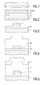
- a first embodiment of the magnetic head according to the invention as well as a method of manufacturing this embodiment will be described with reference to Figs. 1 to 16.
- the method starts from a plane substrate 1 of ferrite, in this example an NiZn ferrite.
- An insulation layer 5a of A1 2 0 3 is formed, for example, by means of sputtering deposition on a substrate face 3a obtained by polishing.
- Si0 2 may be used instead of A1 2 0 3 .
- an adhesive layer 7a of Mo, a layer 7b of Au and an adhesive layer 7c of Mo are successively deposited, for example by means of sputtering on the layer 5a for forming a test and/or bias winding 7.
- An insulation layer 5b of, for example A1 2 0 3 is provided, for example by means of sputtering on the layer 5a and the winding 7 on this layer.
- the layers 5a and 5b jointly constitute a relatively thick layer 5 of a non-magnetic material.
- a layer 9 of Mo is provided, for example by means of sputtering deposition on the layer 5 which is present on the substrate 1, whereafter Mo is removed in two areas 11 a and 11 by means of etching. Subsequently, a sputter-etching operation is performed in which the layer 9 functions as a mask and in which two recesses 15a and 15b are formed in the main layers 5.
- a layer 17 of a soil-magnetic material is provided on the layer 5 thus structured, with the recesses 15a and 15b being filled up for forming two flux-guiding elements 17a and 17b.
- the layer 17 is formed by sputtering deposition of a FeNbSi alloy.
- a FeNbSi alloy instead of a FeNbSi alloy, it is alternatively possible to use a CoZrNb alloy, a FeSiAI alloy or an NiFe alloy.
- the soil-magnetic material from which the flux-guiding elements are formed have a relatively high to high relative magnetic permeability which is roughly between 100 and 2000.
- a polishing treatment is carried out.
- a thin electrically insulating, magnetic intermediate layer 21 having a relative magnetic permeability of between 1.1 and 25 is formed on the main face 19 which is preferably obtained by means of mechanochemical polishing.
- the method described in European Patent Application no. 93200995.4 (PHN 14.428; herewith incorporated by reference) is preferably used in this case.
- the intermediate layer 21 has a relative permeability ⁇ r of 5.
- a layer 23a of a magnetoresistive material is formed on the intermediate layer 21, for which purpose an alloy of NiFe is sputtered in this example.
- the layer 23a is subsequently structured by means of a photoresist mask and etching to form a magnetoresistive element (MR element) 23.
- MR element magnetoresistive element
- the MR element 23 bridges the distance between the two flux-guiding elements 17a and 17b, with peripheral areas 23b ad 23c of the MR element 23 being present opposite the elements 17a and 17b and being magnetically coupled to the flux-guiding elements via said intermediate layer 21.
- a layer 25a of an electrically conducting material, for example Au is provided on the MR element 23, which layer is structured by means of a photoresist mask and etching to form equipotential strips 25 of a barberpole structure and to form electrically conducting strips 25b for the electrical connection of the MR element to a measuring device (not shown).
- a insulation layer 27 of, for example A1 2 0 3 is provided by means of, for example sputtering deposition.
- Apertures 29 extending as far as the conducting strips 25b so as to render electrical connections possible are etched in this insulation layer, whereafter a protective counterblock 31 of, for example BaTi0 3 or CaTi0 3 is secured by means of, for example an adhesive agent.
- the layer 27 may be planed in advance to the desired thickness, for example by means of mechanical polishing.
- processing operations for example grinding, the unit now obtained is provided with a head face 33 for cooperation with a magnetic recording medium, particularly a magnetic tape.
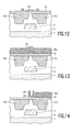
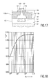
- Fig. 17 shows a second embodiment of the magnetic head according to the invention.
- This magnetic head has a head face 133 and comprises a thin-film structure provided on a ferrite substrate 101.
- the thin-film structure comprises as its main elements a magnetoresistive element (MR element) 123 oriented transversely of the head face 133 and a flux-guiding element 117a terminating in the head face 133, while an electrically insulating intermediate layer 121 having a magnetic permeability of between 1 and 25 extends between a peripheral portion 123a, which is parallel to the head face 133, of the MR element 123 and the flux-guiding element 117a.
- MR element magnetoresistive element
- the intermediate layer 121 which is formed from an oxidic soft-magnetic material, in this example an MgMnZn ferrite, and preferably has a relative permeability ⁇ r of between 2 and approximately 10, is directly provided on the magnetically well-conducting flux-guiding element 117a and has a thickness d of between 0.1 and 1.0 ⁇ m. In this example the layer thickness is 3 ⁇ m.
- the peripheral portion 123a is present on said intermediate layer 121.
- the thin-film structure may have a further flux-guiding element 117b which is magnetically coupled to the MR element via the same intermediate layer (now denoted by the reference numeral 122) of a relatively low relative permeability.
- a bias winding 107 may also be present.
- the thin-film structure further comprises electrically insulating, non-magnetic insulation layers 104, 105 and 106.
- Fig. 18 shows the computed efficiency of an embodiment of the thin-film magnetic head according to the invention as a function of the relative magnetic permeability ⁇ r of the intermediate layer.
- the magnetic head according to the invention also comprises an embodiment in which the magnetoresistive element adjoins the head face and the flux-guiding element which is present is spaced apart therefrom or an embodiment having a magnetoresistive element without a so-called barberpole structure.
Landscapes
- Engineering & Computer Science (AREA)
- Manufacturing & Machinery (AREA)
- Magnetic Heads (AREA)
Applications Claiming Priority (2)
| Application Number | Priority Date | Filing Date | Title |
|---|---|---|---|
| BE9301284 | 1993-11-22 | ||
| BE9301284A BE1007775A3 (nl) | 1993-11-22 | 1993-11-22 | Magneetkop, voorzien van een kopvlak en een dunnefilm structuur, en werkwijze voor het vervaardigen van de magneetkop. |
Publications (3)
| Publication Number | Publication Date |
|---|---|
| EP0654782A2 true EP0654782A2 (de) | 1995-05-24 |
| EP0654782A3 EP0654782A3 (en) | 1995-06-21 |
| EP0654782B1 EP0654782B1 (de) | 1999-07-07 |
Family
ID=3887569
Family Applications (1)
| Application Number | Title | Priority Date | Filing Date |
|---|---|---|---|
| EP94203349A Expired - Lifetime EP0654782B1 (de) | 1993-11-22 | 1994-11-17 | Magnetkopf mit einer Kopfseite und einer Dünnfilmstruktur und Magnetkopfherstellungsverfahren |
Country Status (5)
| Country | Link |
|---|---|
| US (1) | US6233126B1 (de) |
| EP (1) | EP0654782B1 (de) |
| JP (1) | JPH07192228A (de) |
| BE (1) | BE1007775A3 (de) |
| DE (1) | DE69419390T2 (de) |
Cited By (2)
| Publication number | Priority date | Publication date | Assignee | Title |
|---|---|---|---|---|
| WO1997036289A1 (en) * | 1996-03-27 | 1997-10-02 | Philips Electronics N.V. | Magnetic head with uninterrupted flux guide |
| US6223420B1 (en) | 1998-12-04 | 2001-05-01 | International Business Machines Corporation | Method of making a read head with high resistance soft magnetic flux guide layer for enhancing read sensor efficiency |
Families Citing this family (2)
| Publication number | Priority date | Publication date | Assignee | Title |
|---|---|---|---|---|
| US7683445B2 (en) * | 2005-02-24 | 2010-03-23 | Everspin Technologies, Inc. | Enhanced permeability device structures and method |
| US7285835B2 (en) * | 2005-02-24 | 2007-10-23 | Freescale Semiconductor, Inc. | Low power magnetoelectronic device structures utilizing enhanced permeability materials |
Family Cites Families (9)
| Publication number | Priority date | Publication date | Assignee | Title |
|---|---|---|---|---|
| NL7901578A (nl) | 1979-02-28 | 1980-09-01 | Philips Nv | Magnetoweerstandkop. |
| JPS5977618A (ja) * | 1982-10-27 | 1984-05-04 | Sony Corp | 磁気抵抗効果形磁気ヘツド |
| JPS59111929A (ja) | 1982-12-15 | 1984-06-28 | Masanori Abe | フエライト膜作製方法 |
| JPH0664718B2 (ja) * | 1985-07-01 | 1994-08-22 | 株式会社東芝 | 薄膜磁気ヘツド |
| JPH07105006B2 (ja) * | 1985-11-05 | 1995-11-13 | ソニー株式会社 | 磁気抵抗効果型磁気ヘツド |
| US4754354A (en) | 1986-05-05 | 1988-06-28 | Eastman Kodak Company | Ferrite film insulating layer in a yoke-type magneto-resistive head |
| JP2507710B2 (ja) * | 1986-08-20 | 1996-06-19 | 関西日本電気株式会社 | ヨ−ク型薄膜磁気ヘツド |
| JPH056515A (ja) * | 1991-06-28 | 1993-01-14 | Hitachi Ltd | 薄膜磁気ヘツド |
| JP2740586B2 (ja) * | 1991-08-12 | 1998-04-15 | アルプス電気株式会社 | 薄膜磁気ヘッド |
-
1993
- 1993-11-22 BE BE9301284A patent/BE1007775A3/nl not_active IP Right Cessation
-
1994
- 1994-11-17 DE DE69419390T patent/DE69419390T2/de not_active Expired - Fee Related
- 1994-11-17 EP EP94203349A patent/EP0654782B1/de not_active Expired - Lifetime
- 1994-11-21 JP JP6286354A patent/JPH07192228A/ja active Pending
-
1996
- 1996-08-15 US US08/698,193 patent/US6233126B1/en not_active Expired - Fee Related
Cited By (3)
| Publication number | Priority date | Publication date | Assignee | Title |
|---|---|---|---|---|
| WO1997036289A1 (en) * | 1996-03-27 | 1997-10-02 | Philips Electronics N.V. | Magnetic head with uninterrupted flux guide |
| US6223420B1 (en) | 1998-12-04 | 2001-05-01 | International Business Machines Corporation | Method of making a read head with high resistance soft magnetic flux guide layer for enhancing read sensor efficiency |
| US6873499B2 (en) | 1998-12-04 | 2005-03-29 | International Business Machines Corporation | Read head having high resistance soft magnetic flux guide layer for enhancing read sensor efficiency |
Also Published As
| Publication number | Publication date |
|---|---|
| BE1007775A3 (nl) | 1995-10-17 |
| US6233126B1 (en) | 2001-05-15 |
| DE69419390T2 (de) | 2000-02-17 |
| EP0654782B1 (de) | 1999-07-07 |
| EP0654782A3 (en) | 1995-06-21 |
| JPH07192228A (ja) | 1995-07-28 |
| DE69419390D1 (de) | 1999-08-12 |
Similar Documents
| Publication | Publication Date | Title |
|---|---|---|
| EP0881627A2 (de) | Dünnfilmmagnetkopf | |
| US5843521A (en) | Photoresist frame plated magnetic transducer pole layer employing high magnetic permeability seed layer | |
| EP0521564B1 (de) | Dünnfilmmagnetkopf | |
| EP0269129B1 (de) | Dünnfilmmagnetkopf | |
| JP2002032903A (ja) | 垂直磁気記録用薄膜磁気ヘッド | |
| EP0204902B1 (de) | Magnetischer Wandlerkopf mit Joch und Nutzung eines Magnetwiderstandseffekts | |
| EP0171956B1 (de) | Mit Permanentmagnet vormagnetisierter magnetoresistiver Wandler für Schmalspuraufnahme | |
| EP0675486A2 (de) | Magnetoresistiver Wandler mit integriertem Joch und magnetischem Nebenschluss | |
| EP0663661A1 (de) | Dualer magnetoresistiver Wiedergabekopf mit magnetischer Abschirmung und Verfahren zu seiner Herstellung | |
| EP0702357B1 (de) | Magnetowiderstandeffektkopf und Magnetaufzeichnungs-/Wiedergabekopf daraus | |
| EP0654782B1 (de) | Magnetkopf mit einer Kopfseite und einer Dünnfilmstruktur und Magnetkopfherstellungsverfahren | |
| US4907115A (en) | Super conducting thin-film magnetic head including a magnetoresistive element | |
| US4768121A (en) | Magnetic head formed by composite main pole film and winding core for perpendicular magnetic recording | |
| US4700253A (en) | Slanted pole head for magnetic recording | |
| US6842314B2 (en) | Magnetoresistive device and method of manufacturing same, and thin-film magnetic head and method of manufacturing same | |
| EP0514976B1 (de) | Kombinierter Lese-/Schreibe-Magnetkopf | |
| CA1179771A (en) | Perpendicular mode magnetic transducer head | |
| US6028749A (en) | Magnetic head having a multilayer structure and method of manufacturing the magnetic head | |
| EP0482642B1 (de) | Zusammengesetzter magnetoresistiver Dünnfilmmagnetkopf | |
| EP0582342B1 (de) | Magnetkopf mit einer Mehrschichtstruktur und Verfahren zum Herstellen des Magnetkopfes | |
| EP0770991A2 (de) | Dünnfilmmagnetoresistiver Kopf mit aneinandergrenzendem Übergang | |
| KR100307860B1 (ko) | 박막자기헤드및자기헤드제조방법 | |
| EP0600549B1 (de) | Verfahren zur Herstellung eines Dünnfilmmagnetkopfes und Kopf erhalten durch das Verfahren | |
| JP2507710B2 (ja) | ヨ−ク型薄膜磁気ヘツド | |
| US6205007B1 (en) | Thin-film magnetic head and method of manufacturing the magnetic head |
Legal Events
| Date | Code | Title | Description |
|---|---|---|---|
| PUAI | Public reference made under article 153(3) epc to a published international application that has entered the european phase |
Free format text: ORIGINAL CODE: 0009012 |
|
| PUAL | Search report despatched |
Free format text: ORIGINAL CODE: 0009013 |
|
| AK | Designated contracting states |
Kind code of ref document: A2 Designated state(s): DE FR GB |
|
| AK | Designated contracting states |
Kind code of ref document: A3 Designated state(s): DE FR GB |
|
| 17P | Request for examination filed |
Effective date: 19951221 |
|
| GRAG | Despatch of communication of intention to grant |
Free format text: ORIGINAL CODE: EPIDOS AGRA |
|
| 17Q | First examination report despatched |
Effective date: 19980922 |
|
| GRAG | Despatch of communication of intention to grant |
Free format text: ORIGINAL CODE: EPIDOS AGRA |
|
| GRAH | Despatch of communication of intention to grant a patent |
Free format text: ORIGINAL CODE: EPIDOS IGRA |
|
| GRAH | Despatch of communication of intention to grant a patent |
Free format text: ORIGINAL CODE: EPIDOS IGRA |
|
| GRAA | (expected) grant |
Free format text: ORIGINAL CODE: 0009210 |
|
| AK | Designated contracting states |
Kind code of ref document: B1 Designated state(s): DE FR GB |
|
| REF | Corresponds to: |
Ref document number: 69419390 Country of ref document: DE Date of ref document: 19990812 |
|
| ET | Fr: translation filed | ||
| PLBE | No opposition filed within time limit |
Free format text: ORIGINAL CODE: 0009261 |
|
| STAA | Information on the status of an ep patent application or granted ep patent |
Free format text: STATUS: NO OPPOSITION FILED WITHIN TIME LIMIT |
|
| 26N | No opposition filed | ||
| PGFP | Annual fee paid to national office [announced via postgrant information from national office to epo] |
Ref country code: FR Payment date: 20001121 Year of fee payment: 7 |
|
| PGFP | Annual fee paid to national office [announced via postgrant information from national office to epo] |
Ref country code: GB Payment date: 20001129 Year of fee payment: 7 |
|
| PGFP | Annual fee paid to national office [announced via postgrant information from national office to epo] |
Ref country code: DE Payment date: 20010118 Year of fee payment: 7 |
|
| PG25 | Lapsed in a contracting state [announced via postgrant information from national office to epo] |
Ref country code: GB Free format text: LAPSE BECAUSE OF NON-PAYMENT OF DUE FEES Effective date: 20011117 |
|
| REG | Reference to a national code |
Ref country code: GB Ref legal event code: IF02 |
|
| PG25 | Lapsed in a contracting state [announced via postgrant information from national office to epo] |
Ref country code: DE Free format text: LAPSE BECAUSE OF NON-PAYMENT OF DUE FEES Effective date: 20020702 |
|
| GBPC | Gb: european patent ceased through non-payment of renewal fee |
Effective date: 20011117 |
|
| PG25 | Lapsed in a contracting state [announced via postgrant information from national office to epo] |
Ref country code: FR Free format text: LAPSE BECAUSE OF NON-PAYMENT OF DUE FEES Effective date: 20020730 |
|
| REG | Reference to a national code |
Ref country code: FR Ref legal event code: ST |
|
| REG | Reference to a national code |
Ref country code: FR Ref legal event code: ST |