EP0654825B1 - Dispositif de détection de rayonnement, à éléments de détection aboutés, et procédé de fabrication de ce dispositif - Google Patents
Dispositif de détection de rayonnement, à éléments de détection aboutés, et procédé de fabrication de ce dispositif Download PDFInfo
- Publication number
- EP0654825B1 EP0654825B1 EP94402589A EP94402589A EP0654825B1 EP 0654825 B1 EP0654825 B1 EP 0654825B1 EP 94402589 A EP94402589 A EP 94402589A EP 94402589 A EP94402589 A EP 94402589A EP 0654825 B1 EP0654825 B1 EP 0654825B1
- Authority
- EP
- European Patent Office
- Prior art keywords
- elements
- photodetectors
- detection
- complimentary
- substrate
- Prior art date
- Legal status (The legal status is an assumption and is not a legal conclusion. Google has not performed a legal analysis and makes no representation as to the accuracy of the status listed.)
- Expired - Lifetime
Links
Images


Classifications
-
- H—ELECTRICITY
- H10—SEMICONDUCTOR DEVICES; ELECTRIC SOLID-STATE DEVICES NOT OTHERWISE PROVIDED FOR
- H10F—INORGANIC SEMICONDUCTOR DEVICES SENSITIVE TO INFRARED RADIATION, LIGHT, ELECTROMAGNETIC RADIATION OF SHORTER WAVELENGTH OR CORPUSCULAR RADIATION
- H10F39/00—Integrated devices, or assemblies of multiple devices, comprising at least one element covered by group H10F30/00, e.g. radiation detectors comprising photodiode arrays
- H10F39/10—Integrated devices
- H10F39/12—Image sensors
-
- H—ELECTRICITY
- H10—SEMICONDUCTOR DEVICES; ELECTRIC SOLID-STATE DEVICES NOT OTHERWISE PROVIDED FOR
- H10F—INORGANIC SEMICONDUCTOR DEVICES SENSITIVE TO INFRARED RADIATION, LIGHT, ELECTROMAGNETIC RADIATION OF SHORTER WAVELENGTH OR CORPUSCULAR RADIATION
- H10F39/00—Integrated devices, or assemblies of multiple devices, comprising at least one element covered by group H10F30/00, e.g. radiation detectors comprising photodiode arrays
- H10F39/10—Integrated devices
- H10F39/12—Image sensors
- H10F39/18—Complementary metal-oxide-semiconductor [CMOS] image sensors; Photodiode array image sensors
- H10F39/184—Infrared image sensors
- H10F39/1843—Infrared image sensors of the hybrid type
Definitions
- the present invention relates to a radiation detection device, with elements successful detection, as well as a manufacturing process of this device.
- the invention applies in particular to the production of linear optical detection bars very long linear, especially for thermal imaging.
- This technique consists of juxtaposing, on an interconnection substrate, arrays elementary photodetectors, without loss of pixels, the total size of the equivalent bar not being then more limited by the factors mentioned more high, namely the defect rate and limited size substrates on which we manufacture the photodetectors.
- One of the possible butting techniques consists in manufacturing detection elements, or components, comprising photodetectors, or pixels, and cut off the ends of these components at most near their end pixels so you can mechanically juxtapose these components while retaining the detection step.
- hybridization technique flip-chip
- the components receive the radiation to be detected by their rear faces.
- the major difficulty of this kind of technique is to cut the components without degrading the pixels located near the edge of the cutouts (because inevitable mechanical stresses by cutting).
- Figure 1A is a schematic view of two detection elements 2 and 4 butted and hybridized on an interconnection network support 6 according to this flip-chip hybridization technique.
- Figure 1B is section I-I of figure 1A.
- Figures 1A and 1B show electrically conductive microbeads 12 allowing the hybridization of elements 2 and 4 on the support 6 as well as the connection of photodetectors 8 and 10 to connection conductors 14 associated with them on support 6.
- the reference D represents the (optical) size of the photodetectors (which are for example photodiodes) and the reference g represents the minimum distance between two adjacent cutting edges, this distance being imposed by mechanical considerations (precision of cutting, placement accuracy of adjacent chips).
- the present invention aims to remedy the previous disadvantages by proposing a device for photodetection likely to have a very large length as well as a manufacturing process for this device, the invention avoiding the degradation of pixels of the photodetection elements close to the edges cutouts.
- the present invention has relates to a radiation detection device, this device comprising at least two elements of successful detection, each element being made of material transparent to radiation and having, on a face, a plurality of photodetectors capable of detecting radiation, this device being characterized in that that it further includes, for any set of two butted elements, a detection element complementary having, on one side, a plurality of photodetectors capable of detecting radiation, in this that this additional element is placed astride the two butted elements, the photodetectors of this complementary element facing said faces of these two butted elements, and in that these two butted elements do not include any photodetector in look of the photodetectors of the complementary element.
- this further comprises a substrate comprising at least one hole, this hole being able to receive the complementary element, the two elements abutments are hybridized on the substrate by balls electrically conductive and the sensing element complementary is connected to the substrate by through electrical connections formed on electrically butted and ball elements conductive.
- the substrate can include a single drilling, suitable for receiving each additional element, or a plurality of holes, each of these being able to receive an additional element.
- Each of the abutting elements as well as the corresponding complementary element can understand a row of step photodetectors determined, the number of photodetectors of the element being chosen so as to obtain, when this additional element is placed astride the corresponding butted elements, a single row of photodetectors having said determined pitch.
- the present invention allows a butting (without geometrical limitation of the size of photodetectors) of an unlimited number of detection.
- the invention also allows the pitch of photodetectors is equal to D (optical size of photodetectors).
- the invention further makes it possible to move away from a chosen distance the edges of the edges of the first useful photodetectors.
- the radiation detection device according to the invention which is schematically shown in Figures 2A to 2D, results from a three-dimensional hybridization of elements of photodetection.
- the device of the figures 2A to 2D includes a plurality of detection elements (two in the example shown), which bear references 16 and 18 respectively, as well as a interconnection network support 20.
- Each of elements 16 and 18 is made of material transparent to R radiation to be detected and a, on one side, a row of photodetectors capable of detect this radiation (for example, photodiodes).
- the photodetectors of element 16 carry reference 22 while the photodetectors of element 18 has the reference 24.
- the device of FIGS. 2A to 2D comprises further an additional detection element 26 which has, on one side, a row of suitable photodetectors 28 to detect radiation and this complementary element is placed astride the two elements 16 and 18 abutted.
- the photodetectors 28 of this element 26 are opposite the faces of the two elements 16 and 18, faces on which the photodetectors are formed 22 and 24.
- the detection elements 16 and 18 are butted as standard on the substrate interconnection 20.
- the elements 16 and 18 are hybridized by solder balls on the substrate 20 and the element complementary 26 is itself hybridized on the elements 16 and 18 by solder balls, through a longitudinal bore 30 which the support of interconnection network.
- the photodetectors 28 of element 26 are connected to the interconnection network support 20 by through electrical connections, which are formed on elements 16 and 18, and balls of welding.
- the complementary detection element 26 includes, in the example shown, more than two photodetectors.
- the more the additional element includes photodetectors (replacing photodetectors of butted elements) and the more it is possible to move away the cutting edges of these abutting elements of the first photodetectors of these detection elements.
- the radiation R to be detected passes through these elements 16 and 18 to illuminate the photodetectors of the complementary element 26 (which constitutes a sort detection bridge).
- a device in accordance with the invention constituted by a strip of 2000 pixels with a pixel pitch P of 25 ⁇ m; the optical size D of the pixels is 18 ⁇ m and the minimum geometric distance g between two cutting edges is 3 ⁇ m.
- Each photodetector of element 18 like for example the photodetector 24 (FIG. 2B), is provided with an electrical connecting conductor 32 located on the corresponding element and is associated with a conductor electrical connection 34 arranged on the support interconnection network 20, these conductors 32 and 34 being electrically connected via a solder ball 36, these balls 36 being in the vicinity of an edge of the bore 30 in the example shown.
- solder balls 38 located at near the other edge of this hole, are respectively placed opposite the balls 36 and allow the element 18 to be fixed to the support 20.
- Each photodetector 28 of the element complementary 26 ( Figure 2C) is provided with a conductor electrical connection 40 placed on the front panel of element 26 and associated with an electrical conductor link 34 placed on the support 20.
- Another connecting electrical conductor 44 is associated with this conductor 40 and placed on the face front of the photodetection element 16 opposite from which the photodetector 28 is located.
- a solder ball 46 makes it possible to connect the conductor 40 to conductor 44 and the latter is connected to conductor 34 via a ball of weld 36, as seen in Figure 2C.
- the embodiment of the solder balls is good known in the state of the art.
- These balls can be, for example, produced by electrolytic growth of a layer of low melting material over a surface wettable (for example a gold surface).
- Balls 36 and 38 are produced on the interconnection network support 20, which can be silicon, alumina or any other material suitable for this kind of substrate (the drilling of which is carried out way known in the state of the art).
- Balls 46 and 50 are produced on the elements 16 and 18 and / or the complementary element 26.
- the hybridization of element 26 is done at through hole 30.
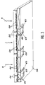
- Another device according to the invention is schematically represented in perspective on the Figure 3 and includes a plurality of elements of detection butted 56 and hybridized on a support of interconnection network 58.
- the support 58 includes holes 60 in look at the junctions of butted elements 56 and additional detection elements 62 are placed in these holes.
- Each element 56 (which is made of a material transparent to R radiation to be detected) includes a row of photodetectors 64 and each complementary element 62 comprises a plurality of photodetectors 66, on its face which is opposite the faces of butted elements 56, faces on which find the photodetectors 64.
- These elements 56 have no photodetector opposite photodetectors 66 of additional elements 62.
- each complementary element 62 has only two photodetectors 66.
- support 58 has only one longitudinal drilling in which the additional elements 62.
Landscapes
- Photometry And Measurement Of Optical Pulse Characteristics (AREA)
- Solid State Image Pick-Up Elements (AREA)
- Measurement Of Radiation (AREA)
- Radiation Pyrometers (AREA)
- Light Receiving Elements (AREA)
Description
"Recent developments on 12.5 µm infrared detection buttable linear arrays", dont les auteurs sont J.P. Chamonal, C. Lucas, P. Bouchut, D. Blachier et P. Angelbaut, publié dans Proceedings of SPIE Infrared Detectors and Focal Plane Arrays, vol.1685, à la date du 23 Avril 1992.
- on fabrique le substrat pourvu dudit perçage,
- on réalise l'hybridation des éléments de détection aboutés sur ce substrat, et
- on assemble l'élément complémentaire à la structure ainsi obtenue, à travers le perçage du substrat.
- la figure 1A est une vue de dessus schématique d'un dispositif de détection de rayonnement connu et a déjà été décrite,
- la figure 1B est la coupe I-I de la figure 1A et a déjà été décrite,
- la figure 2A est une vue de dessus schématique d'un dispositif de détection de rayonnement conforme à l'invention,
- la figure 2B est la coupe II-II de la figure 2A,
- la figure 2C est la coupe III-III de la figure 2A,
- la figure 2D est la coupe IV-IV de la figure 2A, et
- la figure 3 est une vue en perspective schématique et partielle d'un autre dispositif de détection conforme à l'invention.
Claims (5)
- Dispositif de détection de rayonnement, ce dispositif comprenant au moins deux éléments de détection aboutés (16, 18; 56), chaque élément étant fait d'un matériau transparent au rayonnement et ayant, sur une face, une pluralité de photodétecteurs (22, 24; 64) aptes à détecter le rayonnement, ce dispositif étant caractérisé en ce qu'il comprend en outre, pour tout ensemble de deux éléments aboutés, un élément de détection complémentaire (26; 62) ayant, sur une face, une pluralité de photodétecteurs (28; 66) aptes à détecter le rayonnement, en ce que cet élément complémentaire est placé à cheval sur les deux éléments aboutés, les photodétecteurs de cet élément complémentaire étant en regard desdites faces de ces deux éléments aboutés, et en ce que ces deux éléments aboutés ne comportent aucun photodétecteur en regard des photodétecteurs de l'élément complémentaire.
- Dispositif selon la revendication 1, caractérisé en ce qu'il comprend en outre un substrat (20; 58) comportant au moins un perçage (30; 60), ce perçage étant apte à recevoir l'élément complémentaire, en ce que les deux éléments aboutés sont hybridés sur le substrat par des billes électriquement conductrices (36, 38) et en ce que l'élément de détection complémentaire est relié au substrat par l'intermédiaire de connexions électriques (44) formées sur les éléments aboutés et de billes électriquement conductrices (36, 46).
- Dispositif selon la revendication 2, caractérisé en ce que le substrat comprend un seul perçage (30), apte à recevoir chaque élément complémentaire (26), ou une pluralité de perçages (60), chacun de ceux-ci étant apte à recevoir un élément complémentaire (62).
- Dispositif selon l'une quelconque des revendications 1 à 3, caractérisé en ce que chacun des éléments aboutés ainsi que l'élément complémentaire correspondant comprennent une rangée de photodétecteurs de pas déterminé, et en ce que le nombre de photodétecteurs de l'élément complémentaire est choisi de façon à obtenir, lorsque cet élément complémentaire est placé à cheval sur les éléments aboutés correspondants, une rangée unique de photodétecteurs ayant ledit pas déterminé.
- Procédé de fabrication du dispositif selon la revendication 2, caractérisé en ce qu'il comprend les étapes suivantes :on fabrique le substrat (20) pourvu dudit perçage (30),on réalise l'hybridation des éléments de détection aboutés (16, 18) sur ce substrat, eton assemble l'élément complémentaire (26) à la structure ainsi obtenue, à travers le perçage (30) du substrat (20).
Applications Claiming Priority (2)
| Application Number | Priority Date | Filing Date | Title |
|---|---|---|---|
| FR9313721 | 1993-11-17 | ||
| FR9313721A FR2712693B1 (fr) | 1993-11-17 | 1993-11-17 | Dispositif de détection de rayonnement, à éléments de détection aboutés, et procédé de fabrication de ce dispositif. |
Publications (2)
| Publication Number | Publication Date |
|---|---|
| EP0654825A1 EP0654825A1 (fr) | 1995-05-24 |
| EP0654825B1 true EP0654825B1 (fr) | 1999-03-24 |
Family
ID=9452939
Family Applications (1)
| Application Number | Title | Priority Date | Filing Date |
|---|---|---|---|
| EP94402589A Expired - Lifetime EP0654825B1 (fr) | 1993-11-17 | 1994-11-16 | Dispositif de détection de rayonnement, à éléments de détection aboutés, et procédé de fabrication de ce dispositif |
Country Status (5)
| Country | Link |
|---|---|
| US (1) | US5591959A (fr) |
| EP (1) | EP0654825B1 (fr) |
| JP (1) | JPH07218337A (fr) |
| DE (1) | DE69417351T2 (fr) |
| FR (1) | FR2712693B1 (fr) |
Families Citing this family (19)
| Publication number | Priority date | Publication date | Assignee | Title |
|---|---|---|---|---|
| KR100438256B1 (ko) * | 1995-12-18 | 2004-08-25 | 마츠시타 덴끼 산교 가부시키가이샤 | 반도체장치 및 그 제조방법 |
| US5856914A (en) * | 1996-07-29 | 1999-01-05 | National Semiconductor Corporation | Micro-electronic assembly including a flip-chip mounted micro-device and method |
| GB2318448B (en) | 1996-10-18 | 2002-01-16 | Simage Oy | Imaging detector and method of production |
| US5937014A (en) * | 1997-03-27 | 1999-08-10 | Telefonaktiebolaget Lm Ericsson | Self-synchronizing equalization techniques and systems |
| US6459084B1 (en) | 1997-05-30 | 2002-10-01 | University Of Central Florida | Area receiver with antenna-coupled infrared sensors |
| US6091138A (en) * | 1998-02-27 | 2000-07-18 | Advanced Micro Devices, Inc. | Multi-chip packaging using bump technology |
| US6380563B2 (en) | 1998-03-30 | 2002-04-30 | Micron Technology, Inc. | Opto-electric mounting apparatus |
| US6713788B2 (en) * | 1998-03-30 | 2004-03-30 | Micron Technology, Inc. | Opto-electric mounting apparatus |
| US6232667B1 (en) | 1999-06-29 | 2001-05-15 | International Business Machines Corporation | Technique for underfilling stacked chips on a cavity MLC module |
| US6369448B1 (en) | 2000-01-21 | 2002-04-09 | Lsi Logic Corporation | Vertically integrated flip chip semiconductor package |
| US6351027B1 (en) * | 2000-02-29 | 2002-02-26 | Agilent Technologies, Inc. | Chip-mounted enclosure |
| US6828545B1 (en) * | 2001-05-15 | 2004-12-07 | Raytheon Company | Hybrid microelectronic array structure having electrically isolated supported islands, and its fabrication |
| FR2838565B1 (fr) * | 2002-04-12 | 2004-06-25 | Commissariat Energie Atomique | Matrice de photodetecteurs, a pixels isoles et grille de stockage, hybridee sur un circuit de lecture |
| US20040012094A1 (en) * | 2002-07-18 | 2004-01-22 | Harper Timothy V. | Flip-chip integrated circuit package and method of assembly |
| US20100248269A1 (en) * | 2009-03-30 | 2010-09-30 | New York Blood Center | Detection of fibrin and fibrinogen degradation products and associated methods of production and use for the detection and monitoring of cancer |
| DE102009060217B3 (de) | 2009-12-23 | 2011-06-22 | Pyreos Ltd. | Verfahren zum Herstellen eines Infrarotlichtdetektors |
| DE102010061182B4 (de) * | 2010-12-13 | 2013-02-07 | Presens Precision Sensing Gmbh | Sensoranordnung, Verfahren und Messsystem zur Erfassung der Verteilung wenigstens einer Veränderlichen eines Objekts |
| CN103415758A (zh) * | 2011-02-18 | 2013-11-27 | 日本电气株式会社 | 红外检测传感器阵列以及红外检测装置 |
| FR3149130A1 (fr) * | 2023-05-24 | 2024-11-29 | Airbus Defence And Space Sas | Circuit de lecture pour capteur hybride |
Family Cites Families (12)
| Publication number | Priority date | Publication date | Assignee | Title |
|---|---|---|---|---|
| US4463262A (en) * | 1981-09-21 | 1984-07-31 | The United States Of America As Represented By The Secretary Of The Air Force | Thick film radiation detector |
| JPS61135280A (ja) * | 1984-12-06 | 1986-06-23 | Toshiba Corp | 三次元撮像素子 |
| JPH0654802B2 (ja) * | 1985-04-05 | 1994-07-20 | セイコーエプソン株式会社 | 固体撮像装置 |
| FR2581251B1 (fr) * | 1985-04-30 | 1987-09-11 | Thomson Csf | Dispositif d'aboutement optique de detecteurs photosensibles |
| US4695861A (en) * | 1985-10-21 | 1987-09-22 | Honeywell Inc. | Backside mosaic photoconductive infrared detector array |
| US4695716A (en) * | 1985-12-13 | 1987-09-22 | Xerox Corporation | Image sensor array for assembly with like arrays to form a longer array |
| US4807021A (en) * | 1986-03-10 | 1989-02-21 | Kabushiki Kaisha Toshiba | Semiconductor device having stacking structure |
| FR2644632B1 (fr) * | 1988-04-22 | 1994-06-17 | Commissariat Energie Atomique | Element de detection constitue de barrettes de detecteurs |
| US4987295A (en) * | 1989-03-31 | 1991-01-22 | General Electric Company | Multichip imager with improved optical performance near the butt region |
| US5065245A (en) * | 1990-04-30 | 1991-11-12 | Eastman Kodak Company | Modular image sensor array |
| US5120960A (en) * | 1991-04-25 | 1992-06-09 | Westinghouse Electric Corp. | Infrared image detecting device and method |
| US5313055A (en) * | 1991-09-30 | 1994-05-17 | Fuji Xerox Co., Ltd. | Two-dimensional image read/display device |
-
1993
- 1993-11-17 FR FR9313721A patent/FR2712693B1/fr not_active Expired - Fee Related
-
1994
- 1994-10-27 US US08/331,369 patent/US5591959A/en not_active Expired - Fee Related
- 1994-11-15 JP JP6304207A patent/JPH07218337A/ja not_active Withdrawn
- 1994-11-16 EP EP94402589A patent/EP0654825B1/fr not_active Expired - Lifetime
- 1994-11-16 DE DE69417351T patent/DE69417351T2/de not_active Expired - Fee Related
Non-Patent Citations (2)
| Title |
|---|
| 231 757 (SEIKO EPSON) 16 Octobre 1986 * |
| PATENT ABSTRACTS OF JAPAN vol. 11, no. 77 (E-487) (2524) 7 Mars 1987 & JP-A-61 * |
Also Published As
| Publication number | Publication date |
|---|---|
| JPH07218337A (ja) | 1995-08-18 |
| EP0654825A1 (fr) | 1995-05-24 |
| DE69417351T2 (de) | 1999-10-07 |
| DE69417351D1 (de) | 1999-04-29 |
| US5591959A (en) | 1997-01-07 |
| FR2712693A1 (fr) | 1995-05-24 |
| FR2712693B1 (fr) | 1995-12-15 |
Similar Documents
| Publication | Publication Date | Title |
|---|---|---|
| EP0654825B1 (fr) | Dispositif de détection de rayonnement, à éléments de détection aboutés, et procédé de fabrication de ce dispositif | |
| EP0702850B1 (fr) | Composant hybride semiconducteur | |
| EP0828452B1 (fr) | Dispositif capteur d'empreintes | |
| EP0645654B1 (fr) | Procédés de réalisation d'une structure intégrée monolithique incorporant des composants opto-électroniques et structures ainsi réalisées | |
| FR2734083A1 (fr) | Module optique integre comportant un guide d'ondes et un dispositif de photoreception, et son procede de fabrication | |
| FR2571901A1 (fr) | Laser a semi-conducteur et procede de fabrication d'un tel laser ou les parties photodetectrices sont formees sur le support semi-conducteur | |
| EP0860724A1 (fr) | Procédé d'assemblage d'un dispositif opto-hybride | |
| WO2001073492A1 (fr) | Procede et dispositif d'alignement passif de fibres optiques et de composants optoelectroniques | |
| EP1322966A1 (fr) | Connecteur electrique a contacts multiples | |
| EP4020600A1 (fr) | Procédé de mise en courbure collective de composants microélectroniques | |
| FR2630550A1 (fr) | Procede de montage d'elements optiques sur un support et circuit optique ainsi obtenu | |
| EP0703473A1 (fr) | Dispositif optoélectronique intégrant un récepteur multilongeur d'onde perfectionné | |
| EP3696865B1 (fr) | Photodiode | |
| FR2713017A1 (fr) | Détecteur de rayonnements dans deux bandes de longueurs d'ondes et procédé de fabrication de ce détecteur. | |
| EP1639808B1 (fr) | Capteur d image a barrettes lineaires aboutees | |
| EP0828413B1 (fr) | Dispositif d'affichage électro-optique et support flexible pour de tels dispositifs servant à l'alimentation de ces dispositifs | |
| EP4481480A1 (fr) | Commutateur à base de matériau à changement de phase | |
| EP4350890A1 (fr) | Commutateur a base d'un materiau a changement de phase | |
| EP1429166A1 (fr) | Arrangement optique à deux entrées/sorties optiques et un procédé de fabrication | |
| FR2823859A1 (fr) | Support de positionnement et de maintien de fibres optiques et son procede de realisation | |
| FR2795199A1 (fr) | Dispositif et procede de fabrication de dispositifs comprenant au moins une puce montee sur un support | |
| WO2022129278A1 (fr) | Interconnecteur pour chaînes de cellules solaires destinées à former un module photovoltaïque | |
| EP0064918A2 (fr) | Détecteur de rayonnement à photodiodes mesa | |
| FR2860347A1 (fr) | Connecteur electrique a au moins deux contacts | |
| FR2798010A1 (fr) | Composant electro-optique multi-sections |
Legal Events
| Date | Code | Title | Description |
|---|---|---|---|
| PUAI | Public reference made under article 153(3) epc to a published international application that has entered the european phase |
Free format text: ORIGINAL CODE: 0009012 |
|
| AK | Designated contracting states |
Kind code of ref document: A1 Designated state(s): DE GB IT |
|
| 17P | Request for examination filed |
Effective date: 19951031 |
|
| GRAG | Despatch of communication of intention to grant |
Free format text: ORIGINAL CODE: EPIDOS AGRA |
|
| 17Q | First examination report despatched |
Effective date: 19980119 |
|
| GRAG | Despatch of communication of intention to grant |
Free format text: ORIGINAL CODE: EPIDOS AGRA |
|
| GRAH | Despatch of communication of intention to grant a patent |
Free format text: ORIGINAL CODE: EPIDOS IGRA |
|
| GRAH | Despatch of communication of intention to grant a patent |
Free format text: ORIGINAL CODE: EPIDOS IGRA |
|
| GRAA | (expected) grant |
Free format text: ORIGINAL CODE: 0009210 |
|
| AK | Designated contracting states |
Kind code of ref document: B1 Designated state(s): DE GB IT |
|
| PG25 | Lapsed in a contracting state [announced via postgrant information from national office to epo] |
Ref country code: IT Free format text: LAPSE BECAUSE OF FAILURE TO SUBMIT A TRANSLATION OF THE DESCRIPTION OR TO PAY THE FEE WITHIN THE PRE;WARNING: LAPSES OF ITALIAN PATENTS WITH EFFECTIVE DATE BEFORE 2007 MAY HAVE OCCURRED AT ANY TIME BEFORE 2007. THE CORRECT EFFECTIVE DATE MAY BE DIFFERENT FROM THE ONE RECORDED.SCRIBED TIME-LIMIT Effective date: 19990324 |
|
| REF | Corresponds to: |
Ref document number: 69417351 Country of ref document: DE Date of ref document: 19990429 |
|
| GBT | Gb: translation of ep patent filed (gb section 77(6)(a)/1977) |
Effective date: 19990527 |
|
| PG25 | Lapsed in a contracting state [announced via postgrant information from national office to epo] |
Ref country code: GB Free format text: LAPSE BECAUSE OF NON-PAYMENT OF DUE FEES Effective date: 19991116 |
|
| PLBE | No opposition filed within time limit |
Free format text: ORIGINAL CODE: 0009261 |
|
| STAA | Information on the status of an ep patent application or granted ep patent |
Free format text: STATUS: NO OPPOSITION FILED WITHIN TIME LIMIT |
|
| 26N | No opposition filed | ||
| GBPC | Gb: european patent ceased through non-payment of renewal fee |
Effective date: 19991116 |
|
| PG25 | Lapsed in a contracting state [announced via postgrant information from national office to epo] |
Ref country code: DE Free format text: LAPSE BECAUSE OF NON-PAYMENT OF DUE FEES Effective date: 20000901 |