EP0654835A1 - Magnetoresistives Material enthaltender Gegenstand - Google Patents
Magnetoresistives Material enthaltender Gegenstand Download PDFInfo
- Publication number
- EP0654835A1 EP0654835A1 EP94308245A EP94308245A EP0654835A1 EP 0654835 A1 EP0654835 A1 EP 0654835A1 EP 94308245 A EP94308245 A EP 94308245A EP 94308245 A EP94308245 A EP 94308245A EP 0654835 A1 EP0654835 A1 EP 0654835A1
- Authority
- EP
- European Patent Office
- Prior art keywords
- layer
- temperature
- substrate
- article according
- ratio
- Prior art date
- Legal status (The legal status is an assumption and is not a legal conclusion. Google has not performed a legal analysis and makes no representation as to the accuracy of the status listed.)
- Granted
Links
- 239000000463 material Substances 0.000 title claims abstract description 48
- QVGXLLKOCUKJST-UHFFFAOYSA-N atomic oxygen Chemical compound [O] QVGXLLKOCUKJST-UHFFFAOYSA-N 0.000 claims abstract description 23
- 239000001301 oxygen Substances 0.000 claims abstract description 23
- 229910052760 oxygen Inorganic materials 0.000 claims abstract description 23
- 239000000203 mixture Substances 0.000 claims abstract description 20
- 238000010438 heat treatment Methods 0.000 claims abstract description 18
- 229910052746 lanthanum Inorganic materials 0.000 claims abstract description 4
- 239000000758 substrate Substances 0.000 claims description 33
- VYPSYNLAJGMNEJ-UHFFFAOYSA-N Silicium dioxide Chemical group O=[Si]=O VYPSYNLAJGMNEJ-UHFFFAOYSA-N 0.000 claims description 16
- 239000013078 crystal Substances 0.000 claims description 14
- 230000005291 magnetic effect Effects 0.000 claims description 12
- 238000000034 method Methods 0.000 claims description 12
- 229910052681 coesite Inorganic materials 0.000 claims description 8
- 229910052906 cristobalite Inorganic materials 0.000 claims description 8
- 239000000377 silicon dioxide Substances 0.000 claims description 8
- 235000012239 silicon dioxide Nutrition 0.000 claims description 8
- 229910052682 stishovite Inorganic materials 0.000 claims description 8
- 229910052905 tridymite Inorganic materials 0.000 claims description 8
- 238000000608 laser ablation Methods 0.000 claims description 5
- 239000012080 ambient air Substances 0.000 claims description 3
- 238000004519 manufacturing process Methods 0.000 claims description 3
- 150000001875 compounds Chemical class 0.000 claims description 2
- 230000008569 process Effects 0.000 claims description 2
- 229910002115 bismuth titanate Inorganic materials 0.000 claims 1
- 230000015572 biosynthetic process Effects 0.000 abstract description 2
- 239000010408 film Substances 0.000 description 25
- 238000000151 deposition Methods 0.000 description 9
- 230000008021 deposition Effects 0.000 description 8
- 239000000523 sample Substances 0.000 description 8
- CPLXHLVBOLITMK-UHFFFAOYSA-N Magnesium oxide Chemical compound [Mg]=O CPLXHLVBOLITMK-UHFFFAOYSA-N 0.000 description 7
- 229910001233 yttria-stabilized zirconia Inorganic materials 0.000 description 7
- 229910002244 LaAlO3 Inorganic materials 0.000 description 6
- 230000005415 magnetization Effects 0.000 description 5
- 230000005294 ferromagnetic effect Effects 0.000 description 4
- 229910002370 SrTiO3 Inorganic materials 0.000 description 3
- 238000012545 processing Methods 0.000 description 3
- 239000010409 thin film Substances 0.000 description 3
- XKRFYHLGVUSROY-UHFFFAOYSA-N Argon Chemical compound [Ar] XKRFYHLGVUSROY-UHFFFAOYSA-N 0.000 description 2
- IJGRMHOSHXDMSA-UHFFFAOYSA-N Atomic nitrogen Chemical compound N#N IJGRMHOSHXDMSA-UHFFFAOYSA-N 0.000 description 2
- RTAQQCXQSZGOHL-UHFFFAOYSA-N Titanium Chemical compound [Ti] RTAQQCXQSZGOHL-UHFFFAOYSA-N 0.000 description 2
- 239000003570 air Substances 0.000 description 2
- 238000000265 homogenisation Methods 0.000 description 2
- 239000002184 metal Substances 0.000 description 2
- 229910052751 metal Inorganic materials 0.000 description 2
- 229910003455 mixed metal oxide Inorganic materials 0.000 description 2
- 230000005298 paramagnetic effect Effects 0.000 description 2
- 238000004549 pulsed laser deposition Methods 0.000 description 2
- 229910018663 Mn O Inorganic materials 0.000 description 1
- 229910003176 Mn-O Inorganic materials 0.000 description 1
- 229910016978 MnOx Inorganic materials 0.000 description 1
- 238000002679 ablation Methods 0.000 description 1
- 229910021486 amorphous silicon dioxide Inorganic materials 0.000 description 1
- 229910052786 argon Inorganic materials 0.000 description 1
- 230000008859 change Effects 0.000 description 1
- 238000005229 chemical vapour deposition Methods 0.000 description 1
- 229910052804 chromium Inorganic materials 0.000 description 1
- 238000007796 conventional method Methods 0.000 description 1
- 229910052802 copper Inorganic materials 0.000 description 1
- RKTYLMNFRDHKIL-UHFFFAOYSA-N copper;5,10,15,20-tetraphenylporphyrin-22,24-diide Chemical compound [Cu+2].C1=CC(C(=C2C=CC([N-]2)=C(C=2C=CC=CC=2)C=2C=CC(N=2)=C(C=2C=CC=CC=2)C2=CC=C3[N-]2)C=2C=CC=CC=2)=NC1=C3C1=CC=CC=C1 RKTYLMNFRDHKIL-UHFFFAOYSA-N 0.000 description 1
- 238000013461 design Methods 0.000 description 1
- 238000000407 epitaxy Methods 0.000 description 1
- 238000001704 evaporation Methods 0.000 description 1
- 230000008020 evaporation Effects 0.000 description 1
- 238000002474 experimental method Methods 0.000 description 1
- 239000003302 ferromagnetic material Substances 0.000 description 1
- 230000005307 ferromagnetism Effects 0.000 description 1
- PCHJSUWPFVWCPO-UHFFFAOYSA-N gold Chemical compound [Au] PCHJSUWPFVWCPO-UHFFFAOYSA-N 0.000 description 1
- 239000010931 gold Substances 0.000 description 1
- 229910052737 gold Inorganic materials 0.000 description 1
- 238000011065 in-situ storage Methods 0.000 description 1
- 230000003993 interaction Effects 0.000 description 1
- 238000007737 ion beam deposition Methods 0.000 description 1
- 239000007788 liquid Substances 0.000 description 1
- 238000005259 measurement Methods 0.000 description 1
- 230000007246 mechanism Effects 0.000 description 1
- 230000008018 melting Effects 0.000 description 1
- 238000002844 melting Methods 0.000 description 1
- 238000001451 molecular beam epitaxy Methods 0.000 description 1
- 229910021421 monocrystalline silicon Inorganic materials 0.000 description 1
- 229910052757 nitrogen Inorganic materials 0.000 description 1
- 238000005457 optimization Methods 0.000 description 1
- 229910000889 permalloy Inorganic materials 0.000 description 1
- 231100000572 poisoning Toxicity 0.000 description 1
- 230000000607 poisoning effect Effects 0.000 description 1
- 239000011148 porous material Substances 0.000 description 1
- 238000011160 research Methods 0.000 description 1
- 238000012552 review Methods 0.000 description 1
- 238000005001 rutherford backscattering spectroscopy Methods 0.000 description 1
- 230000035945 sensitivity Effects 0.000 description 1
- 238000005245 sintering Methods 0.000 description 1
- 238000004544 sputter deposition Methods 0.000 description 1
Images


Classifications
-
- H—ELECTRICITY
- H10—SEMICONDUCTOR DEVICES; ELECTRIC SOLID-STATE DEVICES NOT OTHERWISE PROVIDED FOR
- H10N—ELECTRIC SOLID-STATE DEVICES NOT OTHERWISE PROVIDED FOR
- H10N50/00—Galvanomagnetic devices
- H10N50/80—Constructional details
- H10N50/85—Materials of the active region
-
- Y—GENERAL TAGGING OF NEW TECHNOLOGICAL DEVELOPMENTS; GENERAL TAGGING OF CROSS-SECTIONAL TECHNOLOGIES SPANNING OVER SEVERAL SECTIONS OF THE IPC; TECHNICAL SUBJECTS COVERED BY FORMER USPC CROSS-REFERENCE ART COLLECTIONS [XRACs] AND DIGESTS
- Y10—TECHNICAL SUBJECTS COVERED BY FORMER USPC
- Y10S—TECHNICAL SUBJECTS COVERED BY FORMER USPC CROSS-REFERENCE ART COLLECTIONS [XRACs] AND DIGESTS
- Y10S428/00—Stock material or miscellaneous articles
- Y10S428/90—Magnetic feature
-
- Y—GENERAL TAGGING OF NEW TECHNOLOGICAL DEVELOPMENTS; GENERAL TAGGING OF CROSS-SECTIONAL TECHNOLOGIES SPANNING OVER SEVERAL SECTIONS OF THE IPC; TECHNICAL SUBJECTS COVERED BY FORMER USPC CROSS-REFERENCE ART COLLECTIONS [XRACs] AND DIGESTS
- Y10—TECHNICAL SUBJECTS COVERED BY FORMER USPC
- Y10S—TECHNICAL SUBJECTS COVERED BY FORMER USPC CROSS-REFERENCE ART COLLECTIONS [XRACs] AND DIGESTS
- Y10S428/00—Stock material or miscellaneous articles
- Y10S428/922—Static electricity metal bleed-off metallic stock
- Y10S428/9265—Special properties
- Y10S428/928—Magnetic property
-
- Y—GENERAL TAGGING OF NEW TECHNOLOGICAL DEVELOPMENTS; GENERAL TAGGING OF CROSS-SECTIONAL TECHNOLOGIES SPANNING OVER SEVERAL SECTIONS OF THE IPC; TECHNICAL SUBJECTS COVERED BY FORMER USPC CROSS-REFERENCE ART COLLECTIONS [XRACs] AND DIGESTS
- Y10—TECHNICAL SUBJECTS COVERED BY FORMER USPC
- Y10T—TECHNICAL SUBJECTS COVERED BY FORMER US CLASSIFICATION
- Y10T428/00—Stock material or miscellaneous articles
- Y10T428/11—Magnetic recording head
- Y10T428/1107—Magnetoresistive
Definitions
- This invention pertains to magnetoresistive materials, and to articles (e.g., a magnetic field probe or a recording head) that comprise the material.
- the "magnetoresistance" (MR) of a material is the resistance R(H) of the material in an applied magnetic field H minus the resistance R o in the absence of an applied field.
- the Helmholt et al. paper (op. cit.) discloses that a heat treatment (12 hours, 900°C, air) transformed an initially paramagnetic La-Ba-Mn-oxide film into a ferromagnetic one, with increased peak temperature and a sharper peak, and teaches that these improvements are related to homogenization during the heat treatment.
- the invention is embodied in an article that comprises a layer of a material that exhibits magnetoresistance at 25°C and has nominal composition XMnO y , where X is La and at least one of Ca, Sr and Ba.
- the oxygen content (designated by the subscript y) is selected such that the layer of material has, at 25°C, a MR ratio of 200% or more (in absolute value).
- the MR ratio is defined as (R(H) - R o )/R(H), where R(H) is the resistance (or resistivity) of the layer of material in an applied magnetic field H, and R o is the resistance (or resistivity) in the absence of an applied magnetic field.
- the strength of the applied field is 6 Tesla.
- the improved properties of the layer of material are associated with the novel method of making the article.
- the method comprises forming a layer of nominal composition XMnO y' (y' typically different from y) on a substrate (e.g, MgO,SrTiO3, possibly including an intermediate layer) and heat treating the layer.
- a substrate e.g, MgO,SrTiO3, possibly including an intermediate layer
- heat treating the layer is in contact with an atmosphere that comprises oxygen, the partial pressure of oxygen in the atmosphere being greater than the partial pressure of oxygen in ambient air.
- the atmosphere is flowing oxygen at ambient pressure.
- the temperature and duration of the heat treatment are selected such that, after completion of the treatment, the material exhibits a MR ratio of at least 200% (absolute value) at 25°C, in a field of 6T.
- the film is formed on a substrate, possibly a support body (e.g., a Si wafer) with a buffer layer (e.g., MgO) thereon.
- a substrate possibly a support body (e.g., a Si wafer) with a buffer layer (e.g., MgO) thereon.
- a buffer layer e.g., MgO
- substrate materials are MgO, SrTiO3, and LaAlO3.
- FIG. 2 shows the magnetization loop of an exemplary material according to the invention.
- the material was heated 3 hours at 900°C in flowing O2.
- the measurement was made at 280K for experimental reasons.
- the results at 25°C would be very similar.
- FIG. 3 shows exemplary results of MR ratio vs. temperature, for different heat treatment conditions.
- the material has nominal composition La 0.67 Ca 0.33 MnO y (y ⁇ 3).
- Curve 30 pertains to as-deposited material, curve 31 to material that was heated 30 minutes at 700°C in flowing O2, and curve 32 to material that was heated 3 hours at 800°C in flowing O2.
- the data demonstrate a strong dependence of room temperature MR on heat treatment conditions (duration and temperature).
- the data when compared to prior art results, also demonstrate the significant improvements that can be attained by heat treatment in an oxygen-rich atmosphere according to the invention.
- the heat treatment conditions are selected such that the maximum in the magnetoresistance ratio occurs at, or close to, the intended working temperature of the article according to the invention, e.g., 25°C.
- FIGS. 4 and 5 show the resistivity of an exemplary layer at 190K and at (approximately) 25°C, showing MR ratios of about 1400 and 410%, respectively, at 6 Tesla.
- ferromagnetism at room temperature is not an inherent property of layers of the relevant oxides.
- appropriate heat treatment in an O2-rich atmosphere can result in ferromagnetic material. For instance, we have produced a film, of nominal composition La 0.67 Ca 0.33 MnO y that has a Curie temperature of about 350K.
- a significant aspect of making material according to the invention is optimization of the oxygen stoichiometry by heat treatment in an oxygen-rich (O2 partial pressure greater than that of ambient air, preferably about 1 atmosphere, but not excluding O2 pressure greater than 1 atmosphere) atmosphere.
- O2 partial pressure greater than that of ambient air preferably about 1 atmosphere, but not excluding O2 pressure greater than 1 atmosphere
- Layers of oxide according to the invention can be formed by any appropriate process, including laser ablation, sputtering, evaporation, molecular beam epitaxy, ion beam deposition, chemical vapor deposition, and electro-or electroless deposition. Layer thicknesses will typically be in the range 5 nm - 100 ⁇ m, depending on user requirements.
- the layers will typically be formed on a substrate but can be free standing. Layers can be polycrystalline, but will frequently be substantially epitaxial with the substrate. In the latter case, the lattice constant of the substrate (e.g., SrTiO3, MgO, LaAlO3) will be close to (typically within about 5%) that of the desired oxide.
- a buffer layer (or layers) is envisaged. For instance, for some device applications it will frequently be desirable to use a Si body as support body, with an appropriate buffer material (e.g., LaAlO3 or other oxide, or inert metal such as gold) thereon to prevent poisoning of the oxide.
- Layer formation by laser ablation or other appropriate technique will typically involve deposition onto a hot substrate (500-1000°C, preferably about 600-900°C), preferably carried out in an oxygencontaining atmosphere.
- a hot substrate 500-1000°C, preferably about 600-900°C
- the subsequent heat treatment in an oxygen-rich atmosphere will generally involve maintaining the film at a temperature in the range 300-1000°C for an effective time for raising the oxygen content of the material to a level that is associated with the desired MR ratio (i.e., absolute value at least 200%) at 25°C.
- the time will be in the range 10 min-100 hours.
- the preferred temperature is below 850°C, and the preferred time is below 12 hours.
- the Ca content in La-Ca-Mn-oxide is preferably in the range 0.25-0.40
- the Ba content in La-Ba-Mn-oxide is preferably in the range 0.20-0.45
- the Sr content in La-Sr-Mn oxide is preferably in the range 0.18-0.50.
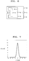
- Oxide layers according to the invention can be incorporated into a variety of devices. Exemplary of such devices is a magnetic field probe, schematically depicted in FIG. 6, wherein numeral 60 refers to a substrate, 61 to a Mn-oxide layer according to the invention, 62 to electrical leads that connect current source 63 to the layer, 64 to electrical leads that connect the layer to volt meter 65.
- FIG. 7 shows resistivity vs. applied magnetic field of an exemplary film of nominal composition La 0.67 Ca 0.33 MnO y that was epitaxial with a LaAlO3 substrate.
- the film was deposited at 700°C in 100 mTorr partial pressure of O2, with a post-deposition treatment of 30 minutes at 900°C in 3 atmospheres O2.
- a film is "epitaxial" with a single crystal substrate if at least one crystallographic axis is common to substrate and film.
- the single crystal substrate need not be a bulk single crystal body such as a Si wafer but can be a substantially single crystal layer on non-single crystal material.
- a substrate that consists of an amorphous layer (e.g., SiO2) on a single crystal Si wafer, with a substantially single crystal Bi-titanate layer on the amorphous layer is a "single crystal” substrate.
- a layer is "substantially" single crystal if the material has preferred c-axis orientation, with FWHM (full width at half maximum) in the c-axis x-ray rocking curve of less than 2°. In many cases, the material will also meet the requirement that ⁇ min is less than 20% (preferably less than 10%), where " ⁇ min " is the well known Rutherford backscattering ratio.
- the film of FIG. 7 was formed by pulsed laser deposition from a relatively dense target.
- a relatively dense target can result in higher quality films with fewer flaws (e.g., particulates and/or pores) and improved epitaxy, and thus is preferred.
- denser target can be prepared by sintering at higher than conventional temperature (e.g., 1300°C vs. 1000-1100°C).
- magnetoresistive material Although it is frequently desirable for magnetoresistive material to have a large MR ratio at or close to room temperature, those skilled in the art will appreciate that, for instance, a material that exhibits a large MR ratio at liquid nitrogen temperature (77K) or above can find wide technological application since such temperatures can be readily and inexpensively attained and maintained. Nevertheless, it is significant that the temperature of maximum resistance can be affected by processing conditions. In particular, we have discovered that a higher (exemplarily >100 m Torr) oxygen partial pressure (p 0 2 ) during deposition tends to result in films with higher temperature of peak resistance. The magnetization, especially near room temperature, also tends to increase with increasing p 0 2 , during deposition.
- p 0 2 oxygen partial pressure
- a La-Ca-Mn-O film deposited at p 0 2 ⁇ 300 mTorr exhibited MR ratios of 1300% and 470% at 260K and 280K, respectively, with magnetization (4 ⁇ M) in excess of 2000 gauss.
- the template layer material is selected to provide a surface of the appropriate crystal symmetry, with at least one epitaxy-relevant lattice dimension close to (typically within ⁇ 8 %) that of the oxide material that is to be deposited thereon.
- An exemplary and currently preferred template material for La-Ca-Mn-Oxide is Bi4Ti3 O x (x ⁇ 12).
- Bi-titanate template layers on SiO2 typically are highly c-axis oriented.
- yttria-stabilized zirconia (YSZ) has a ⁇ 100> lattice parameter of 0.516 nm, close to that of Si (0.545 nm), with about 6% mismatch.
- template materials also have to be mechanically and chemically stable under the processing temperatures, with a melting point above the highest processing temperature.
- a 100 nm thick layer of nominal composition La 0.67 Ca 0.33 MnO y was deposited on a (100) LaAlO3 substrate by laser ablation, using a target of the above composition, about 12 mm diameter and 5 mm thickness. Ablation was carried out in an oxygen atmosphere (100 m Torr). The resulting layer was epitaxial with the substrate and had essentially the same composition as the target. The layer was maintained 30 minutes at 700°C in flowing oxygen (1 atm) in a tube furnace. After removal of the sample from the furnace and cool-down, the resistivity of the layer was measured by a conventional method. The layer exhibited a maximum magnetoresistance ratio of about 1400% in a field of 6T, parallel to the direction of the current in the layer.
- Example 1 A portion of the as-deposited layer of Example 1 was heat treated at 800°C for 30 minutes in flowing oxygen (1 atm). The layer exhibited a magnetoresistance ratio of about 410% near room temperature 25°C in a field of 6T.
- Example 1 A further portion of the as-deposited layer of Example 1 was heat treated as described in Example 2, except that argon was used instead of oxygen.
- the layer exhibited a magnetoresistance ratio of about 7%, and its resistivity was higher than that of the sample of Example 2 by about 4 orders of magnitude.
- the following substrates were provided: a single crystal (100) Si wafer; a single crystal (100) Si wafer with about 100 nm YSZ and 50 nm Bi-titanate (Bi4 Ti3 O x, x ⁇ 12) thereon; and a single crystal (100) Si wafer with about 100 nm amorphous SiO2 thereon, with about 50 nm of Bi-titanate on the SiO2.
- the YSZ and titanate layers were deposited in situ by the previously referred to pulsed laser deposition technique.
- the YSZ layer was highly c-axis oriented and substantially single crystal.
- the titanate layers were highly c-axis textured, with the a-b plane parallel to the substrate surface.
- the substrates were deposited about 100 nm thick films of nominal composition La 0.67 Ca 0.33 MnO y (y ⁇ 3) by laser ablation from a target of the same nominal metal composition, substantially as described in Example 1.
- the substrate temperature during deposition was in the range 600- 700°C, the deposition was carried out under 100 m Torr partial pressure of O2.
- Growth on the Bi4Ti3 O x /YSZ/Si and Bi4Ti3 O x /SiO2/Si substrates was epitaxial. After deposition the films were heat treated at 750°C for 2 hours in O2 (1 atmosphere).
- the MR of the resulting films was measured as a function of temperature by a conventional 4-point probe technique.
- the applied magnetic field was 2T.
- the maximum MR ratios were found to occur at temperatures in the range 110-140K and were less than 30% for the layer on the Si substrate, 80% for the layer on the Bi4Ti3 O x /YSZ/Si substrate, and 1370% for the layer on the Bi4Ti3O x /SiO2/Si substrate.
Landscapes
- Hall/Mr Elements (AREA)
- Thin Magnetic Films (AREA)
- Measuring Magnetic Variables (AREA)
Applications Claiming Priority (4)
| Application Number | Priority Date | Filing Date | Title |
|---|---|---|---|
| US15476693A | 1993-11-18 | 1993-11-18 | |
| US154766 | 1994-04-15 | ||
| US228168 | 1994-04-15 | ||
| US08/228,168 US5549977A (en) | 1993-11-18 | 1994-04-15 | Article comprising magnetoresistive material |
Publications (2)
| Publication Number | Publication Date |
|---|---|
| EP0654835A1 true EP0654835A1 (de) | 1995-05-24 |
| EP0654835B1 EP0654835B1 (de) | 1997-07-16 |
Family
ID=26851760
Family Applications (1)
| Application Number | Title | Priority Date | Filing Date |
|---|---|---|---|
| EP94308245A Expired - Lifetime EP0654835B1 (de) | 1993-11-18 | 1994-11-09 | Verfahren zur Herstellung eines magnetoresistives Material enthaltenden Gegenstands |
Country Status (4)
| Country | Link |
|---|---|
| US (1) | US5549977A (de) |
| EP (1) | EP0654835B1 (de) |
| JP (1) | JP2963354B2 (de) |
| DE (1) | DE69404267T2 (de) |
Cited By (4)
| Publication number | Priority date | Publication date | Assignee | Title |
|---|---|---|---|---|
| ES2128263A1 (es) * | 1997-05-28 | 1999-05-01 | Consejo Superior Investigacion | Dispisitivos magnetoresistivos para la deteccion de presencia y posicion de piezas metalicas. |
| ES2141666A1 (es) * | 1997-10-24 | 2000-03-16 | Consejo Superior Investigacion | Potenciometro modulado magneticamente basado en las propiedades magnetoresistivas de oxidos de manganeso. |
| DE10031229C1 (de) * | 2000-06-23 | 2001-11-22 | Dresden Ev Inst Festkoerper | Stromabhängiges resistives Bauelement |
| DE10110292C1 (de) * | 2001-02-26 | 2002-10-02 | Dresden Ev Inst Festkoerper | Stromabhängiges resistives Bauelement |
Families Citing this family (47)
| Publication number | Priority date | Publication date | Assignee | Title |
|---|---|---|---|---|
| DE69608342T2 (de) * | 1995-03-17 | 2000-10-19 | At & T Corp., New York | Verfahren zur Herstellung eines Gegenstands, welcher aus einem eine Spinellstruktur aufweisenden auf ein Substrat angeordneten Material besteht |
| JP2723082B2 (ja) * | 1995-06-26 | 1998-03-09 | 日本電気株式会社 | 酸化物磁性体及びそれを用いた磁気検出素子 |
| JPH09231523A (ja) * | 1996-02-27 | 1997-09-05 | Nec Corp | 磁気抵抗効果ヘッド |
| US5792569A (en) * | 1996-03-19 | 1998-08-11 | International Business Machines Corporation | Magnetic devices and sensors based on perovskite manganese oxide materials |
| US5840420A (en) * | 1996-03-21 | 1998-11-24 | The University Of Alabama | Magnetoresistance elements exhibiting thermally stable giant magnetoresistance effect |
| US5764056A (en) * | 1996-05-16 | 1998-06-09 | Seagate Technology, Inc. | Nickel-manganese as a pinning layer in spin valve/GMR magnetic sensors |
| US6337991B1 (en) | 1996-11-05 | 2002-01-08 | Corning Applied Technologies Corp. | Large temperature coefficient of resistance material |
| US6117571A (en) * | 1997-03-28 | 2000-09-12 | Advanced Technology Materials, Inc. | Compositions and method for forming doped A-site deficient thin-film manganate layers on a substrate |
| US5856008A (en) * | 1997-06-05 | 1999-01-05 | Lucent Technologies Inc. | Article comprising magnetoresistive material |
| US5854587A (en) * | 1997-06-26 | 1998-12-29 | The United States Of America As Represented By The Secretary Of The Navy | REx M1-x Mny O.sub.δ films for microbolometer-based IR focal plane arrays |
| US6134090A (en) * | 1998-03-20 | 2000-10-17 | Seagate Technology Llc | Enhanced spin-valve/GMR magnetic sensor with an insulating boundary layer |
| US6356420B1 (en) | 1998-05-07 | 2002-03-12 | Seagate Technology Llc | Storage system having read head utilizing GMR and AMr effects |
| US6392257B1 (en) | 2000-02-10 | 2002-05-21 | Motorola Inc. | Semiconductor structure, semiconductor device, communicating device, integrated circuit, and process for fabricating the same |
| US6693033B2 (en) | 2000-02-10 | 2004-02-17 | Motorola, Inc. | Method of removing an amorphous oxide from a monocrystalline surface |
| KR20030011083A (ko) | 2000-05-31 | 2003-02-06 | 모토로라 인코포레이티드 | 반도체 디바이스 및 이를 제조하기 위한 방법 |
| US6501973B1 (en) | 2000-06-30 | 2002-12-31 | Motorola, Inc. | Apparatus and method for measuring selected physical condition of an animate subject |
| US6590236B1 (en) * | 2000-07-24 | 2003-07-08 | Motorola, Inc. | Semiconductor structure for use with high-frequency signals |
| WO2002009187A2 (en) | 2000-07-24 | 2002-01-31 | Motorola, Inc. | Heterojunction tunneling diodes and process for fabricating same |
| US6555946B1 (en) | 2000-07-24 | 2003-04-29 | Motorola, Inc. | Acoustic wave device and process for forming the same |
| US6493497B1 (en) | 2000-09-26 | 2002-12-10 | Motorola, Inc. | Electro-optic structure and process for fabricating same |
| US6638838B1 (en) | 2000-10-02 | 2003-10-28 | Motorola, Inc. | Semiconductor structure including a partially annealed layer and method of forming the same |
| US6501121B1 (en) | 2000-11-15 | 2002-12-31 | Motorola, Inc. | Semiconductor structure |
| US6559471B2 (en) | 2000-12-08 | 2003-05-06 | Motorola, Inc. | Quantum well infrared photodetector and method for fabricating same |
| US20020096683A1 (en) | 2001-01-19 | 2002-07-25 | Motorola, Inc. | Structure and method for fabricating GaN devices utilizing the formation of a compliant substrate |
| US6673646B2 (en) | 2001-02-28 | 2004-01-06 | Motorola, Inc. | Growth of compound semiconductor structures on patterned oxide films and process for fabricating same |
| WO2002082551A1 (en) | 2001-04-02 | 2002-10-17 | Motorola, Inc. | A semiconductor structure exhibiting reduced leakage current |
| US6709989B2 (en) | 2001-06-21 | 2004-03-23 | Motorola, Inc. | Method for fabricating a semiconductor structure including a metal oxide interface with silicon |
| US6992321B2 (en) | 2001-07-13 | 2006-01-31 | Motorola, Inc. | Structure and method for fabricating semiconductor structures and devices utilizing piezoelectric materials |
| US6531740B2 (en) | 2001-07-17 | 2003-03-11 | Motorola, Inc. | Integrated impedance matching and stability network |
| US6646293B2 (en) | 2001-07-18 | 2003-11-11 | Motorola, Inc. | Structure for fabricating high electron mobility transistors utilizing the formation of complaint substrates |
| US7019332B2 (en) | 2001-07-20 | 2006-03-28 | Freescale Semiconductor, Inc. | Fabrication of a wavelength locker within a semiconductor structure |
| US6693298B2 (en) | 2001-07-20 | 2004-02-17 | Motorola, Inc. | Structure and method for fabricating epitaxial semiconductor on insulator (SOI) structures and devices utilizing the formation of a compliant substrate for materials used to form same |
| US6498358B1 (en) | 2001-07-20 | 2002-12-24 | Motorola, Inc. | Structure and method for fabricating an electro-optic system having an electrochromic diffraction grating |
| US6855992B2 (en) | 2001-07-24 | 2005-02-15 | Motorola Inc. | Structure and method for fabricating configurable transistor devices utilizing the formation of a compliant substrate for materials used to form the same |
| US6667196B2 (en) | 2001-07-25 | 2003-12-23 | Motorola, Inc. | Method for real-time monitoring and controlling perovskite oxide film growth and semiconductor structure formed using the method |
| US6589856B2 (en) | 2001-08-06 | 2003-07-08 | Motorola, Inc. | Method and apparatus for controlling anti-phase domains in semiconductor structures and devices |
| US6639249B2 (en) | 2001-08-06 | 2003-10-28 | Motorola, Inc. | Structure and method for fabrication for a solid-state lighting device |
| US20030034491A1 (en) | 2001-08-14 | 2003-02-20 | Motorola, Inc. | Structure and method for fabricating semiconductor structures and devices for detecting an object |
| US6673667B2 (en) | 2001-08-15 | 2004-01-06 | Motorola, Inc. | Method for manufacturing a substantially integral monolithic apparatus including a plurality of semiconductor materials |
| US20030071327A1 (en) | 2001-10-17 | 2003-04-17 | Motorola, Inc. | Method and apparatus utilizing monocrystalline insulator |
| US6916717B2 (en) | 2002-05-03 | 2005-07-12 | Motorola, Inc. | Method for growing a monocrystalline oxide layer and for fabricating a semiconductor device on a monocrystalline substrate |
| US7169619B2 (en) | 2002-11-19 | 2007-01-30 | Freescale Semiconductor, Inc. | Method for fabricating semiconductor structures on vicinal substrates using a low temperature, low pressure, alkaline earth metal-rich process |
| US6885065B2 (en) | 2002-11-20 | 2005-04-26 | Freescale Semiconductor, Inc. | Ferromagnetic semiconductor structure and method for forming the same |
| US7020374B2 (en) | 2003-02-03 | 2006-03-28 | Freescale Semiconductor, Inc. | Optical waveguide structure and method for fabricating the same |
| US6965128B2 (en) | 2003-02-03 | 2005-11-15 | Freescale Semiconductor, Inc. | Structure and method for fabricating semiconductor microresonator devices |
| JP2008270677A (ja) * | 2007-04-25 | 2008-11-06 | National Institute For Materials Science | ドープド・ペロブスカイト・マンガナイト単結晶を用いた巨大異方性磁気抵抗素子 |
| WO2020210257A1 (en) | 2019-04-08 | 2020-10-15 | Kepler Computing Inc. | Doped polar layers and semiconductor device incorporating same |
Family Cites Families (5)
| Publication number | Priority date | Publication date | Assignee | Title |
|---|---|---|---|---|
| US4622613A (en) * | 1983-10-07 | 1986-11-11 | Matsushita Electric Industrials Co., Ltd. | Thin film magnetic head |
| MY108176A (en) * | 1991-02-08 | 1996-08-30 | Hitachi Global Storage Tech Netherlands B V | Magnetoresistive sensor based on oscillations in the magnetoresistance |
| US5304975A (en) * | 1991-10-23 | 1994-04-19 | Kabushiki Kaisha Toshiba | Magnetoresistance effect element and magnetoresistance effect sensor |
| US5287238A (en) * | 1992-11-06 | 1994-02-15 | International Business Machines Corporation | Dual spin valve magnetoresistive sensor |
| DE4425356C2 (de) * | 1993-09-29 | 1998-07-02 | Siemens Ag | Magnetoresistiver Sensor unter Verwendung eines Sensormaterials mit perowskitähnlicher Kristallstruktur |
-
1994
- 1994-04-15 US US08/228,168 patent/US5549977A/en not_active Expired - Fee Related
- 1994-11-09 EP EP94308245A patent/EP0654835B1/de not_active Expired - Lifetime
- 1994-11-09 DE DE69404267T patent/DE69404267T2/de not_active Expired - Fee Related
- 1994-11-18 JP JP6308464A patent/JP2963354B2/ja not_active Expired - Fee Related
Non-Patent Citations (2)
| Title |
|---|
| JIN S ET AL: "Thousandfold change in resistivity in magnetoresistive La-Ca-Mn-O films", SCIENCE, 15 APRIL 1994, USA, vol. 264, no. 5157, ISSN 0036-8075, pages 413 - 415, XP000572785, DOI: doi:10.1126/science.264.5157.413 * |
| VON HELMOLT R ET AL: "Giant negative magnetoresistance in perovskitelike La/sub 2/3/Ba/sub 1/3/MnO/sub x/ ferromagnetic films", PHYSICAL REVIEW LETTERS, 4 OCT. 1993, USA, vol. 71, no. 14, ISSN 0031-9007, pages 2331 - 2333 * |
Cited By (4)
| Publication number | Priority date | Publication date | Assignee | Title |
|---|---|---|---|---|
| ES2128263A1 (es) * | 1997-05-28 | 1999-05-01 | Consejo Superior Investigacion | Dispisitivos magnetoresistivos para la deteccion de presencia y posicion de piezas metalicas. |
| ES2141666A1 (es) * | 1997-10-24 | 2000-03-16 | Consejo Superior Investigacion | Potenciometro modulado magneticamente basado en las propiedades magnetoresistivas de oxidos de manganeso. |
| DE10031229C1 (de) * | 2000-06-23 | 2001-11-22 | Dresden Ev Inst Festkoerper | Stromabhängiges resistives Bauelement |
| DE10110292C1 (de) * | 2001-02-26 | 2002-10-02 | Dresden Ev Inst Festkoerper | Stromabhängiges resistives Bauelement |
Also Published As
| Publication number | Publication date |
|---|---|
| DE69404267T2 (de) | 1998-01-15 |
| EP0654835B1 (de) | 1997-07-16 |
| US5549977A (en) | 1996-08-27 |
| JPH07193298A (ja) | 1995-07-28 |
| DE69404267D1 (de) | 1997-08-21 |
| JP2963354B2 (ja) | 1999-10-18 |
Similar Documents
| Publication | Publication Date | Title |
|---|---|---|
| EP0654835B1 (de) | Verfahren zur Herstellung eines magnetoresistives Material enthaltenden Gegenstands | |
| US7252852B1 (en) | Mg-Zn oxide tunnel barriers and method of formation | |
| US7598555B1 (en) | MgO tunnel barriers and method of formation | |
| US7349187B2 (en) | Tunnel barriers based on alkaline earth oxides | |
| KR102628591B1 (ko) | 체적 단축 자기 결정형 이방성을 갖는 자기층의 스핀 전달 토크 스위칭을 위한 장치 및 방법 | |
| US7570463B2 (en) | Magnetic tunnel junctions including crystalline and amorphous tunnel barrier materials | |
| KR102597922B1 (ko) | 스핀 전달 토크의 애플리케이션에 의해 스위칭될 수 있는 호이슬러 화합물의 고도로 텍스처링된 박막 형성용 템플레이팅층 | |
| US6528326B1 (en) | Magnetoresistive device and method for producing the same, and magnetic component | |
| EP0717422B1 (de) | Film mit Austauschkopplung und magnetoresistives Element | |
| US7345855B2 (en) | Tunnel barriers based on rare earth element oxides | |
| Liu et al. | The large magnetoresistance property of La 0.5 Sr 0.5 CoO 3− x thin films prepared by pulsed laser deposition | |
| Wu et al. | Effect of annealing in reduced oxygen pressure on the electrical transport properties of epitaxial thin film and bulk (La 1− x Nd x) 0.7 Sr 0.3 MnO 3 | |
| US5538800A (en) | Magnetoresistive oxide material and articles comprising the material | |
| Ziese et al. | Extrinsic magnetoresistance and resistance relaxation in and films and heterostructures | |
| Krishnan et al. | Role of epitaxy and polycrystallinity in the magnetoresistance and magnetization of La0. 8Sr0. 2MnO3 thin films | |
| Satyalakshmi et al. | Tunneling and enhanced magnetoresistance in Nd 2/3 Sr 1/3 MnO 3 thin films with microcracks | |
| JP3688559B2 (ja) | (La,Ba)MnO3系室温超巨大磁気抵抗材料 | |
| Liu et al. | Barium ferrite (BaFe12O19) thin films prepared by pulsed laser deposition on MgO buffered Si substrates | |
| JP2000357828A (ja) | 強磁性酸化物およびこれを用いた磁気抵抗素子 | |
| EP1003047B1 (de) | Magnetowiderstandseffektelement | |
| Namikawa et al. | Annealing effect on magnetic characteristics on (La, Sr) MnO/sub 3/sputtered films | |
| Satoh et al. | Magnetoresistance of La0. 7Sr0. 3MnO3 Thin Films Grown on Polycrystalline MgO Substrates | |
| Jin | Field-induced conductivity changes in CMR manganites | |
| Nakano et al. | Bias dependent intergrain tunneling in lanthanum manganite thin films | |
| Manako et al. | Thin Film Growth and Magnetotransport Study of (La, Sr) MnO3 |
Legal Events
| Date | Code | Title | Description |
|---|---|---|---|
| PUAI | Public reference made under article 153(3) epc to a published international application that has entered the european phase |
Free format text: ORIGINAL CODE: 0009012 |
|
| AK | Designated contracting states |
Kind code of ref document: A1 Designated state(s): DE FR GB |
|
| 17P | Request for examination filed |
Effective date: 19951109 |
|
| 17Q | First examination report despatched |
Effective date: 19960409 |
|
| GRAG | Despatch of communication of intention to grant |
Free format text: ORIGINAL CODE: EPIDOS AGRA |
|
| GRAH | Despatch of communication of intention to grant a patent |
Free format text: ORIGINAL CODE: EPIDOS IGRA |
|
| GRAH | Despatch of communication of intention to grant a patent |
Free format text: ORIGINAL CODE: EPIDOS IGRA |
|
| GRAA | (expected) grant |
Free format text: ORIGINAL CODE: 0009210 |
|
| AK | Designated contracting states |
Kind code of ref document: B1 Designated state(s): DE FR GB |
|
| REF | Corresponds to: |
Ref document number: 69404267 Country of ref document: DE Date of ref document: 19970821 |
|
| ET | Fr: translation filed | ||
| PLBE | No opposition filed within time limit |
Free format text: ORIGINAL CODE: 0009261 |
|
| STAA | Information on the status of an ep patent application or granted ep patent |
Free format text: STATUS: NO OPPOSITION FILED WITHIN TIME LIMIT |
|
| 26N | No opposition filed | ||
| REG | Reference to a national code |
Ref country code: GB Ref legal event code: IF02 |
|
| PGFP | Annual fee paid to national office [announced via postgrant information from national office to epo] |
Ref country code: DE Payment date: 20061102 Year of fee payment: 13 |
|
| PGFP | Annual fee paid to national office [announced via postgrant information from national office to epo] |
Ref country code: GB Payment date: 20061108 Year of fee payment: 13 Ref country code: FR Payment date: 20061108 Year of fee payment: 13 |
|
| GBPC | Gb: european patent ceased through non-payment of renewal fee |
Effective date: 20071109 |
|
| PG25 | Lapsed in a contracting state [announced via postgrant information from national office to epo] |
Ref country code: DE Free format text: LAPSE BECAUSE OF NON-PAYMENT OF DUE FEES Effective date: 20080603 |
|
| REG | Reference to a national code |
Ref country code: FR Ref legal event code: ST Effective date: 20080930 |
|
| PG25 | Lapsed in a contracting state [announced via postgrant information from national office to epo] |
Ref country code: GB Free format text: LAPSE BECAUSE OF NON-PAYMENT OF DUE FEES Effective date: 20071109 |
|
| PG25 | Lapsed in a contracting state [announced via postgrant information from national office to epo] |
Ref country code: FR Free format text: LAPSE BECAUSE OF NON-PAYMENT OF DUE FEES Effective date: 20071130 |