EP0654898A2 - Circuit de transmission - Google Patents
Circuit de transmission Download PDFInfo
- Publication number
- EP0654898A2 EP0654898A2 EP94118229A EP94118229A EP0654898A2 EP 0654898 A2 EP0654898 A2 EP 0654898A2 EP 94118229 A EP94118229 A EP 94118229A EP 94118229 A EP94118229 A EP 94118229A EP 0654898 A2 EP0654898 A2 EP 0654898A2
- Authority
- EP
- European Patent Office
- Prior art keywords
- signal
- output
- output signal
- circuit
- transmission circuit
- Prior art date
- Legal status (The legal status is an assumption and is not a legal conclusion. Google has not performed a legal analysis and makes no representation as to the accuracy of the status listed.)
- Granted
Links
Images


Classifications
-
- H—ELECTRICITY
- H03—ELECTRONIC CIRCUITRY
- H03G—CONTROL OF AMPLIFICATION
- H03G3/00—Gain control in amplifiers or frequency changers
- H03G3/20—Automatic control
- H03G3/30—Automatic control in amplifiers having semiconductor devices
- H03G3/3036—Automatic control in amplifiers having semiconductor devices in high-frequency amplifiers or in frequency-changers
- H03G3/3042—Automatic control in amplifiers having semiconductor devices in high-frequency amplifiers or in frequency-changers in modulators, frequency-changers, transmitters or power amplifiers
- H03G3/3047—Automatic control in amplifiers having semiconductor devices in high-frequency amplifiers or in frequency-changers in modulators, frequency-changers, transmitters or power amplifiers for intermittent signals, e.g. burst signals
-
- H—ELECTRICITY
- H03—ELECTRONIC CIRCUITRY
- H03G—CONTROL OF AMPLIFICATION
- H03G3/00—Gain control in amplifiers or frequency changers
- H03G3/20—Automatic control
- H03G3/30—Automatic control in amplifiers having semiconductor devices
- H03G3/3036—Automatic control in amplifiers having semiconductor devices in high-frequency amplifiers or in frequency-changers
- H03G3/3042—Automatic control in amplifiers having semiconductor devices in high-frequency amplifiers or in frequency-changers in modulators, frequency-changers, transmitters or power amplifiers
Definitions
- This invention relates to a transmission circuit for use in a radio transmitter, such as, that used in the field of mobile radio communication.
- Fig. 1 is a block diagram showing the structure of a prior art transmission circuit.
- the prior art transmission circuit includes a power amplifier circuit 1, an output monitor circuit 2, an output detector circuit 3, an error detector circuit 4, a reference signal generator circuit 5, a high-frequency signal input terminal 6, a gain control terminal 7 and a transmission output terminal 8.
- a high-frequency signal inputted through the high-frequency signal input terminal 6 is amplified by the power amplifier circuit 1, and, after being then branched by the output monitor circuit 2, part of the amplified high-frequency signal is outputted from the transmission output terminal 8.
- the remaining part of the amplified high-frequency signal is inputted to the output detector circuit 3, and the output signal V DET ofthe output detector circuit 3 is inputted to the error detector circuit 4.
- the detected voltage signal V DET is compared with a reference signal V REF generated from the reference signal generator circuit 5 to detect the error voltage, and the detected error voltage signal is then inputted to the power amplifier circuit 1 through the gain control terminal 7 so as to control the gain of the power amplifier circuit 1.
- the high-frequency signal inputted through the high-frequency input terminal 6 of the transmission circuit having the structure as described above is a linear modulated signal whose amplitude carries some kind of information
- this manner of loop control will cancel the modulation when the reference signal V REF is a constant voltage.
- the prior art transmission circuit has had the problem that its output waveform tends to be distorted.
- the transmission circuit according to the present invention which attains the above object comprises an output detector circuit subjecting part of the output signal of the transmission circuit to envelope detection, a peak hold circuit successively holding the peaks of the output signal of the output detector circuit, and an error detector circuit comparing the output signal of the peak hold circuit with a reference signal to generate the error signal used for controlling the gain of a power amplifier circuit.
- part of the output signal of the transmission circuit is subjected to envelope detection by the output detector circuit, and the output signal of the output detector circuit is inputted to the peak hold circuit successively holding the peaks of the output signal of the output detector circuit, so that the peak level of the output signal of the transmission circuit is detected as a DC value. Therefore, even when the reference signal is a constant voltage, the modulation would not be cancelled by the loop control, and the transmission circuit can operate to exhibit the desired satisfactory transmission performance.
- FIG. 2 is a block diagram showing the structure of the first embodiment of the transmission circuit according to the present invention
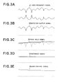
- Figs. 3A to 3E show waveforms of various signals appearing in the transmission circuit shown in Fig. 2.
- the transmission circuit comprises a power amplifier circuit 11 amplifying a high-frequency signal 21, an output monitor circuit 12 deriving part of the output signal of the transmission circuit, an output detector circuit 13 subjecting a monitor signal, which is the output signal of the output monitor circuit 12, to envelope detection, a peak hold circuit 14 successively holding the peaks of a detector output signal 22, an error detector circuit 15 comparing the output signal of the peak hold circuit 14 with a reference signal V REF generated from a reference signal generator circuit 16 thereby generating the error voltage, a gain control terminal 17 of the power amplifier circuit 11, a high-frequency signal input terminal 18, and a transmission output terminal 19.
- a high-frequency signal 21 having a waveform as shown in Fig. 3A is inputted through the high-frequency signal input terminal 18 to the power amplifier circuit 11 and, after being amplified by the power amplifier circuit 11 and then passed through the output monitor circuit 12, appears at the transmission output terminal 19 as the output signal of the transmission circuit.
- part of the output signal of the transmission circuit is branched by the output monitor circuit 12 to be inputted as the monitor signal to the output detector circuit 13 and, after being detected by the output detector circuit 13, appears as the detector output signal 22 having a waveform as shown in Fig. 3B.
- the detector output signal 22 is inputted to the peak hold circuit 14 generating a peak hold signal 23 successively holding the peaks of the detector output signal 22 and having a waveform as shown in Fig. 3C.
- the peak hold circuit 14 is composed of the combination of, for example, time constant circuits, and its time constant during charging is selected to be small so as to follow the detector output signal 22, while its time constant during discharging is selected to be large so as to hold the peak value.
- the reference signal generator circuit 16 generates the reference signal 24 having a waveform as shown in Fig. 3D so as to set the reference level of the output signal of the transmission circuit.
- the error detector circuit 15 detects an error voltage by comparing the peak hold signal 23 with the reference signal 24 and, after amplifying the error voltage, outputs the error voltage signal.
- This error voltage signal is inputted as a gain control signal 25 having a waveform as shown in Fig. 3E to the power amplifier circuit 11 through the gain control terminal 17 so as to control the gain of the power amplifier circuit 11.
- the gain control signal 25 for controlling the gain of the power amplifier circuit 11 is substantially maintained at a constant level, and undesirable distortion of the output waveform attributable to the loop control would not occur, so that the desired satisfactory transmission performance can be exhibited.
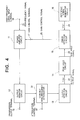
- Fig. 4 is a block diagram showing the structure of a second embodiment of the transmission circuit according to the present invention.
- This second embodiment is a partial modification of the first embodiment shown in Fig. 2, and the same reference numerals are used to designate the same or equivalent parts appearing in Fig. 2 so as to dispense with repetition of the same description.
- This second embodiment differs from the first embodiment in that a variable high-frequency attenuator 31 having an attenuation control terminal 32 is connected between the output monitor circuit 12 and the output detector circuit 13.
- a high-frequency signal 21 is inputted through the high-frequency signal input terminal 18 to the power amplifier circuit 11 and, after being amplified by the power amplifier circuit 11 and then passed through the output monitor circuit 12, appears at the transmission output terminal 19 as the output signal of the transmission circuit.
- part of the output signal of the transmission circuit is branched by the output monitor circuit 12 to be inputted as the monitor signal to the variable high-frequency attenuator 31 and, after being attenuated by a predetermined amount by the attenuation control signal inputted through the attenuation control terminal 32, inputted to the output detector circuit 13 to be detected.
- the detector output signal 22, which is the output signal of the output detector circuit 13, is inputted to the peak hold circuit 14 generating the peak hold signal 23 successively holding the peaks of the detector output signal 22.
- the peak hold circuit 14 is composed of the combination of, for example, time constant circuits, and its time constant during charging is selected to be small so as to follow the detector output signal 22, while its time constant during discharging is selected to be large so as to hold the peak value.
- the reference signal generator circuit 16 generates the reference signal 24 so as to set the reference level of the output signal of the transmission circuit.
- the error detector circuit 15 detects the error voltage by comparing the peak hold signal 23 with the reference signal 24 and, after amplifying the detected error voltage, outputs the error voltage signal. This error voltage signal is inputted as the gain control signal 25 to the power amplifier circuit 11 through the gain control terminal 17 so as to control the gain of the power amplifier circuit 11.
- variable high-frequency attenuator 31 is connected between the output monitor circuit 12 and the output detector circuit 13. Therefore, when, for example, the amount of attenuation by the variable high-frequency attenuator 31 is selected to increase in a relation corresponding to an increase in the value of the output signal of the transmission circuit, the power inputted to the output detector circuit 13 can be maintained at the same level regardless of a change in the value of the output signal of the transmission circuit, so that the range AP of the output signal of the transmission circuit that can be detected within a detected voltage range AV can be widened. That is, regardless of a change in the value of the output signal of the transmission circuit, the proper detected voltage can be always obtained, so that the desired satisfactory loop control can be attained.
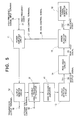
- Fig. 5 is a block diagram showing the structure of a third embodiment of the transmission circuit according to the present invention.
- the third embodiment shown in Fig. 5 is a partial modification of the second embodiment shown in Fig. 4, and the same reference numerals are used to designate the same or equivalent parts so as to dispense with repetition of the same description.
- Waveforms of various signals are the same as those shown in Figs. 3A to 3E.
- This third embodiment differs from the second embodiment in that a high-frequency amplifier 41 is connected between the variable high-frequency attenuator 31 and the output detector circuit 13.
- a high-frequency signal 21 is inputted through the high-frequency input terminal 18 and, after being amplified by the power amplifier circuit 11 and then passed through the output monitor circuit 12, appears at the transmission output terminal 19 as the output signal of the transmission circuit.
- part of the output signal of the transmission circuit is branched by the output monitor circuit 12 to be inputted as the monitor signal to the variable high-frequency attenuator 31 and, after being attenuated by a predetermined amount by the control signal inputted through the attenuation control terminal 32 and amplified by the high-frequency amplifier 41, inputted to the output detector circuit 13 to be detected.
- the detector output signal which is the output signal 22 of the output detector circuit 13, is inputted to the peak hold circuit 14 generating the peak hold signal 23 successively holding the peaks of the detector output signal 22.
- the peak hold circuit 14 is composed of the combination of, for example, time constant circuits, and its time constant during charging is selected to be small so as to follow the detector output signal 22, while its time constant during discharging is selected to be large so as to hold the peak value.
- the reference signal generator circuit 16 generates the reference signal 24 so as to set the reference level of the output signal of the transmission circuit.
- the error detector circuit 15 detects the error voltage by comparing the peak hold signal 23 with the reference signal 24 and, after amplifying the detected error voltage, outputs the error voltage signal. This error voltage signal is inputted as the gain control signal 25 to the power amplifier circuit 11 through the gain control terminal 17 so as to control the gain of the power amplifier circuit 11.
- connection of the high-frequency amplifier 41 between the variable high-frequency attenuator 31 and the output monitor circuit 12 is advantageous in that the transmission circuit can also deal with the case where the monitor signal inputted from the output monitor circuit 12 to the variable high-frequency attenuator 31 is small.
- Fig. 6 shows the structure of a fourth embodiment of the transmission circuit according to the present invention when the present invention is applied to a booster unit adapted to be connected to a portable radio telephone set operable as an independent device so as to amplify a high-frequency signal transmitted from the portable radio telephone set.
- Figs. 7A to 7F show waveforms of various signals appearing in the transmission circuit.
- the reference numerals 51, 52 and 53 designate the portable radio telephone set, the booster unit, and a power supply control terminal connected to a power amplifier circuit 11 in the booster unit 52, respectively and, as for the remaining parts, the same reference numerals are used to designate the same or equivalent parts appearing in Fig. 2 so as to dispense with repetition of the same description.
- a high-frequency signal 61 having a waveform as shown in Fig. 7A is inputted through the high-frequency signal input terminal 18 to be amplified by the power amplifier circuit 11 and is then passed through the output monitor circuit 12 to appear at the transmission output terminal 19 as the output signal of the transmission circuit.
- part of the output signal of the transmission circuit is branched by the output monitor circuit 12 and is inputted as the monitor signal to the output detector circuit 13 to be detected.
- a detector output signal 62 having a waveform as shown in Fig. 7B is inputted to the peak hold circuit 14 generating a peak hold signal 63 successively holding the peaks of the detector output signal 62 and having a waveform as shown in Fig. 7C.
- the peak hold circuit 14 is composed of the combination of, for example, time constant circuits, and its time constant during charging is selected to be small so as to follow the detector output signal 62, while its time constant during discharging is selected to be large so as to hold the peak value.
- the reference signal generator circuit 16 generates a reference signal 64 having a waveform as shown in Fig. 7D so as to set the reference level of the output signal of the transmission circuit.
- the error detector circuit 15 detects an error voltage by comparing the peak hold signal 63 with the reference signal 64 and outputs the detected error voltage as an error voltage signal.
- This error voltage signal is inputted as a gain control signal 65 having a waveform as shown in Fig. 7E to the power amplifier circuit 11 through the gain control terminal 17 so as to control the gain of the power amplifier circuit 11.
- a power supply control signal 66 having a waveform as shown in Fig.
- the power supply control terminal 53 is additionally connected to the power amplifier circuit 11, and the output signal of the transmission circuit is on/off controlled by the burst-like power supply control signal 66, so that consumption of unnecessary power can be minimized.
- an attenuator similar to the variable high-frequency attenuator 31 used in the second embodiment may be connected between the output monitor circuit 12 and the output detector circuit 13 or the high-frequency amplifier 41 used in the third embodiment may be connected to such an attenuator.
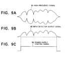
- Fig. 8 is a block diagram showing the structure of a fifth embodiment of the transmission circuit according to the present invention when the present invention is applied to a booster unit adapted to be connected to a portable radio telephone set so as to amplify a high-frequency signal transmitted from the portable radio telephone set.
- Figs. 9A to 9C show waveforms of various signals appearing in the transmission circuit, and Figs. 7B to 7E are also applied to this fifth embodiment of the present invention.
- Fig. 9A to 9C show waveforms of various signals appearing in the transmission circuit, and Figs. 7B to 7E are also applied to this fifth embodiment of the present invention.
- the reference numerals 71, 72, 73, 74 and 75 designate the portable radio telephone set, the booster unit, an input detector circuit, a timing generator circuit, and a power supply control terminal for controlling the power amplifier circuit 11, respectively and, as for the remaining parts, the same reference numerals are used to designate the same or equivalent parts appearing in Fig. 2 so as to dispense with repetition of the same description.
- a high-frequency signal 81 having a waveform as shown in Fig. 9A is inputted through the high-frequency signal input terminal 18 to be amplified by the power amplifier circuit 11 and then passed through the output monitor circuit 12 to appear at the transmission output terminal 19 as the output signal of the transmission circuit.
- part of the output signal of the transmission circuit is branched by the output monitor circuit 12 to be inputted as the monitor signal to the output detector circuit 13 to be detected.
- the detector output signal 62 which is the output signal of the output detector circuit 13, is inputted to the peak hold circuit 14 generating the peak hold signal 63 successively holding the peaks of the detector output signal 62.
- the peak hold circuit 14 is composed of the combination of, for example, time constant circuits, and its time constant during charging is selected to be small so as to follow the detector output signal 62, while its time constant during discharging is selected to be large so as to hold the peak value.
- the reference signal generator circuit 16 generates the reference signal 64 which sets the reference level of the output signal of the transmission circuit.
- the error detector circuit 15 detects the error voltage by comparing the peak hold signal 63 with the reference signal 64 and, after amplifying the detected error voltage, outputs the error voltage signal. This error voltage signal is inputted as the gain control signal 65 to the power amplifier circuit 11 through the gain control terminal 17 so as to control the gain of the power amplifier circuit 11.
- Part of the high-frequency signal 81 inputted through the high-frequency signal input terminal 18 and then branched is inputted to the input detector circuit 73 to be detected.
- An input-detector output signal 82 having a waveform as shown in Fig. 9B is inputted to the timing generator circuit 74 which generates a burst-like output signal turned on/off at certain rising and falling timing of the waveform of the input-detector output signal 82.
- This on/off signal is inputted as a power supply control signal 83 having a waveform as shown in Fig. 9C to the power amplifier circuit 11 through the power supply control terminal 75 so as to control the power supply of the power amplifier circuit 11.
- the burst-like power supply control signal 83 inputted to the power amplifier circuit 11 through the power supply control terminal 75 is generated on the basis of the high-frequency signal 81, so that the signal line extending from the portable radio telephone set 71 is unnecessary, and the above manner of power supply control can minimize consumption of unnecessary power.
- an attenuator similar to the variable high-frequency attenuator 31 used in the second embodiment may be connected between the output monitor circuit 12 and the output detector circuit 13 or the high-frequency amplifier 41 used in the third embodiment may be connected to such an attenuator.
- Fig. 10 is a block diagram showing the structure of a sixth embodiment of the transmission circuit according to the present invention when the present invention is applied to a booster unit adapted for amplifying a high-frequency signal transmitted from the portable radio telephone set.
- the same reference numerals are used to designate the same or equivalent parts appearing in Fig. 8 so as to dispense with repetition of the same description.
- Waveforms of various signals appearing in the transmission circuit are the same as those shown in Figs. 7A to 7F and Figs. 9A to 9C.
- This sixth embodiment differs from the fifth embodiment in that a high-frequency amplifier 91 is connected between the high-frequency signal input terminal 18 and the input detector circuit 73.
- a high-frequency signal 81 inputted through the high-frequency signal input terminal 18 is amplified by the power amplifier circuit 11 and then passed through the output monitor circuit 12 to appear at the transmission output terminal 19 as the output signal of the transmission circuit.
- part of the output signal of the transmission circuit is branched by the output monitor circuit 12 and is inputted as the monitor signal to the output detector circuit 13 to be detected.
- the detector output signal 62 is inputted to the peak hold circuit 14 to appear as the peak hold signal 63 successively holding the peaks of the detector output signal 62.
- the peak hold circuit 14 is composed of the combination of, for example, time constant circuits, and its time constant during charging is selected to be small so as to follow the detector output signal 62, while its time constant during discharging is selected to be large so as to hold the peak value.
- the reference signal generator circuit 16 generates the reference signal 64 which sets the reference level of the output signal of the transmission circuit.
- the error detector circuit 15 detects the error voltage by comparing the peak hold signal 63 with the reference signal 64 and, after amplifying the detected error voltage, outputs the error voltage signal. This error voltage signal is inputted as the gain control signal 65 to the power amplifier circuit 11 through the gain control terminal 17 connected to the power amplifier circuit 11 so as to control the gain of the power amplifier circuit 11.
- Part of the high-frequency signal 81 inputted from the portable radio telephone set 71 through the high-frequency signal input terminal 18 and then branched is inputted, after being amplified by the high-frequency amplifier 91, to the input detector circuit 73 to be detected.
- the input-detector output signal 82 is inputted to the timing generator circuit 74 which generates the burst-like power supply control signal 83 turned on/off at certain rising and falling timing of the waveform of the input-detector output signal 82.
- This power supply control signal 83 is inputted to the power amplifier circuit 11 through the power supply control terminal 75 so as to control the power supply of the power amplifier circuit 11.
- the connection of the high-frequency amplifier 91 between the high-frequency signal input terminal 18 and the input detector circuit 73 is advantageous in that the transmission circuit can also deal with the case where the high-frequency signal 81 is small and, because the low level at the leading edge of the burst signal can be detected, the leading edge of the burst signal can be detected earlier than heretofore so that the desired on/off control of the output signal of the transmission circuit can be reliably attained.
- an attenuator similar to the variable high-frequency attenuator 31 used in the second embodiment may be connected between the output monitor circuit 12 and the output detector circuit 13 or the variable high-frequency amplifier 41 used in the third embodiment may be connected to such an attenuator.
- FIG. 11 is a block diagram showing the structure of the seventh embodiment of the transmission circuit according to the present invention
- Figs. 12A to 12D show waveforms of various signals appearing in the transmission circuit.
- the transmission circuit comprises a variable gain control circuit 101, a power amplifier circuit 102, an output monitor circuit 103, a variable high-frequency attenuator 104, an output detector circuit 105, an error detector circuit 106, an input detector circuit 107, an input monitor circuit 108, a high-frequency signal input terminal 109, a transmission output terminal 110, an attenuation control terminal 111 connected to the variable high-frequency attenuator 104, and a gain control terminal 112 of the variable gain control circuit 101.
- a high-frequency signal 121 having a waveform as shown in Fig. 12A is inputted from the portable radio telephone set 114 through the high-frequency signal input terminal 109 and is branched by the input monitor circuit 108.
- the branched part of the high-frequency signal 121 is, after being amplified by the combination of the variable gain control circuit 101 and the power amplifier circuit 102, branched again by the output monitor circuit 103 to appear at the transmission output terminal 110 as the output signal of the transmission circuit.
- part of the output signal of the transmission circuit is branched by the output monitor circuit 103 to be inputted as a monitor signal to the variable high-frequency attenuator 104, and, after being attenuated by a predetermined amount by a control signal inputted through the attenuation control terminal 111, inputted to and detected by the output detector circuit 105 to appear as an output-detector output signal 122 having a waveform as shown in Fig. 12B.
- part of the input signal 121 branched by the input monitor circuit 108 is inputted to and detected by the input detector circuit 107 to appear as an input-detector output signal 123 having a waveform as shown in Fig. 12C.
- the error detector circuit 106 detects an error voltage by comparing the output signal 122 of the output detector circuit 105 with the output signal 123 of the input detector circuit 107 using the latter output signal 123 as a reference signal, and, after amplifying the error voltage, outputs an error voltage signal.
- This error voltage signal is inputted as a gain control signal 124 having a waveform as shown in Fig. 12D to the variable gain control circuit 101 through the gain control terminal 112 so as to control the gain or attenuation.
- the seventh embodiment of the present invention is advantageous in that, even when a modulated wave signal having a varying amplitude is inputted to the transmission circuit, the input signal is detected to provide a reference signal including varying amplitude components, and such a reference signal is used for error detection, so that the desired satisfactory transmission performance can be exhibited without occurrence of undesirable distortion of the output waveform attributable to the loop control.
- Fig. 13 is a block diagram showing the structure of an eighth embodiment of the transmission circuit according to the present invention.
- the same reference numerals are used to designate the same or equivalent parts appearing in Fig. 11 so as to dispense with repetition of the same description.
- Waveforms of various signals appearing in the transmission circuit are the same as those shown in Figs. 12A to 12D.
- This eighth embodiment is a partial modification of the seventh embodiment and differs from the seventh embodiment in that a high-frequency amplifier 131 is connected between the variable high-frequency attenuator 104 and the output detector circuit 105.
- the high-frequency signal 121 inputted from the portable radio telephones set 114 through the high-frequency signal input terminal 109 and then passed through the input monitor circuit 108 is, after being amplified by the combination of the variable gain control circuit 101 and the power amplifier circuit 102, passed through the output monitor circuit 103 to appear at the transmission output terminal 110 as the output signal of the transmission circuit.
- part of the output signal of the transmission circuit is branched by the output monitor circuit 103 to be inputted as the monitor signal to the variable high-frequency attenuator 104 and, after being attenuated by a predetermined amount by the control signal inputted through the attenuation control terminal 111 and amplified by the high-frequency amplifier 131, inputted to and detected by the output detector circuit 105 to appear as the output-detector output signal 122 which is the output signal of the output detector circuit 105. Also, part of the input signal 121 branched by the input monitor circuit 108 is inputted to and detected by the input detector circuit 107 to appear as the input-detector output signal 123 which is the output signal of the input detector circuit 107.
- the error detector circuit 106 detects the error voltage by comparing the output-detector output signal 122 with the input-detector output signal 123 using the latter output signal 123 as the reference signal and, after amplifying the error voltage, outputs the error voltage signal.
- This error voltage signal is inputted as the gain control signal 124 to the variable gain control circuit 101 so as to control the gain or attenuation.
- the eighth embodiment of the present invention in which the high-frequency amplifier 131 is connected between the variable high-frequency attenuator 104 and the output detector circuit 105 is advantageous in that the transmission circuit can also deal with the case where the monitor signal outputted from the output monitor circuit 103 is small.
- Fig. 14 is a block diagram showing the structure of a ninth embodiment of the transmission circuit according to the present invention, and Figs. 15A to 15E show waveforms of various signals appearing in the transmission circuit.
- the ninth embodiment is a partial modification of the seventh embodiment shown in Fig. 11, and the same reference numerals are used to designate the same or equivalent parts appearing in Fig. 11 so as to dispense with repetition of the same description.
- This ninth embodiment differs from the seventh embodiment in that a power supply control terminal 141 is additionally connected to the power amplifier circuit 102.
- a high-frequency signal 151 having a waveform as shown in Fig. 15A is inputted from the portable radio telephone set 114 through the high-frequency signal input terminal 109 and then passed through the input monitor circuit 108.
- the output signal of the input monitor circuit 108 is, after being amplified by the combination of the variable grain control circuit 101 and the power amplifier circuit 102 and passed through the output monitor circuit 103, appears at the transmission output terminal 110 as the output signal of the transmission circuit.
- part of the output signal of the transmission circuit is branched by the output monitor circuit 103 to be inputted as the monitor signal to the variable high-frequency attenuator 104 and, after being attenuated by a predetermined amount by the control signal inputted through the attenuation control terminal 111, inputted to and detected by the output detector circuit 105 to appear as an output-detector output signal 152 having a waveform as shown in Fig. 15B.
- part of the input signal 151 branched by the input monitor circuit 108 is inputted to and detected by the input detector circuit 107 to appear as an input-detector output signal 153 having a waveform as shown in Fig. 15C.
- the error detector circuit 106 detects the error voltage by comparing the output-detector output signal 152 with the input-detector output signal 153 using the latter output signal 153 as the reference signal and, after amplifying the detected error voltage, outputs the error voltage signal.
- This error voltage signal is inputted as a gain control signal 154 having a waveform as shown in Fig. 15D to the variable gain control circuit 101 through the gain control terminal 112 so as to control the gain or attenuation.
- a power supply control signal 155 having a waveform as shown in Fig. 15E and corresponding to a burst-like high-frequency signal inputted from the portable radio telephone set 114 is inputted through the power supply control terminal 141, so that the output signal of the transmission circuit is on/off controlled to minimize consumption of unnecessary power.
- the ninth embodiment of the present invention in which the power supply control terminal 141 is additionally connected to the power amplifier circuit 102 is advantageous in that the output signal of the transmission circuit is on/off controlled by the burst-like power supply control signal 155 so that consumption of unnecessary power can be minimized.
- the high-frequency amplifier 131 may be connected between the variable high-frequency attenuator 104 and the output detector circuit 105 as in the case of the eighth embodiment.
- Fig. 16 is a block diagram showing the structure of a tenth embodiment of the transmission circuit according to the present invention, and Figs. 17A to 17E show waveforms of various signals appearing in the transmission circuit.
- This tenth embodiment is a partial modification of the seventh embodiment shown in Fig. 11, and the same reference numerals are used to designate the same or equivalent parts appearing in Fig. 11 so as to dispense with repetition of the same description.
- This tenth embodiment differs from the seventh embodiment in that a power supply control terminal 161 is additionally connected to the power amplifier circuit 102, and a timing generator circuit 162 receiving the output signal of the input detector circuit 107 as its input signal is additionally provided.
- a high-frequency signal 171 having a waveform as shown in Fig. 17A is inputted from the portable radio telephone set 114 through the high-frequency input terminal 109 and then passed through the input monitor circuit 104.
- the output signal of the input monitor circuit 104 is, after being amplified by the combination of the variable gain control circuit 101 and the power amplifier circuit 102 and passed through the output monitor circuit 103, appears at the transmission output terminal 110 as the output signal of the transmission circuit.
- part of the output signal of the transmission circuit is branched by the output monitor circuit 103 to be inputted as the monitor signal to the variable high-frequency attenuator 104 and, after being attenuated by a predetermined amount by the control signal inputted through the attenuation control terminal 111, inputted to and detected by the output detector circuit 105 to appear as an output-detector output signal 172 having a waveform as shown in Fig. 17B.
- part of the input signal 171 branched by the input monitor circuit 108 is inputted to and detected by the input detector circuit 107 to appear as an input-detector output signal 173 having a waveform as shown in Fig. 17C.
- the error detector circuit 106 detects the error voltage by comparing the output-detector output signal 172 with the input-output signal 173 using the latter output signal 173 as a reference signal and outputs the error voltage signal.
- This error voltage signal is inputted as a gain control signal 175 having a waveform as shown in Fig. 17E to the variable gain control circuit 101 through the gain control terminal 112 so as to control the gain or attenuation.
- the input-detector output signal 173 outputted from the input detector circuit 107 is inputted to the timing generator circuit 162 to appear as a power supply control signal 174 having a waveform as shown in Fig. 17D and turned on/off at certain rising and falling timing of the waveform of the burst-like high-frequency signal 171 inputted from the portable radio telephone set 114.
- This burst-like power supply control signal 174 is inputted through the power supply control terminal 161 to the power amplifier circuit 102 so as to control the power supply of the power amplifier circuit 102.
- the burst-like power control signal 174 inputted to the power amplifier circuit 102 through the power supply control terminal 161 is generated on the basis of the high-frequency signal 171, so that a signal line extending from the portable radio telephone set 114 is unnecessary, and the above manner of power supply control can minimize consumption of unnecessary power.
- the high-frequency amplifier 131 used in the eighth embodiment may be connected between the variable high-frequency attenuator 107 and the output detector circuit 105.
Landscapes
- Transmitters (AREA)
Applications Claiming Priority (6)
| Application Number | Priority Date | Filing Date | Title |
|---|---|---|---|
| JP29016793 | 1993-11-19 | ||
| JP29016693A JPH07143054A (ja) | 1993-11-19 | 1993-11-19 | 送信回路 |
| JP29016693 | 1993-11-19 | ||
| JP290166/93 | 1993-11-19 | ||
| JP290167/93 | 1993-11-19 | ||
| JP5290167A JPH07143057A (ja) | 1993-11-19 | 1993-11-19 | 送信回路 |
Publications (3)
| Publication Number | Publication Date |
|---|---|
| EP0654898A2 true EP0654898A2 (fr) | 1995-05-24 |
| EP0654898A3 EP0654898A3 (fr) | 1996-01-24 |
| EP0654898B1 EP0654898B1 (fr) | 2001-10-10 |
Family
ID=26557919
Family Applications (1)
| Application Number | Title | Priority Date | Filing Date |
|---|---|---|---|
| EP94118229A Expired - Lifetime EP0654898B1 (fr) | 1993-11-19 | 1994-11-18 | Circuit de transmission |
Country Status (4)
| Country | Link |
|---|---|
| US (1) | US5659893A (fr) |
| EP (1) | EP0654898B1 (fr) |
| CA (1) | CA2135816C (fr) |
| DE (1) | DE69428570T2 (fr) |
Cited By (6)
| Publication number | Priority date | Publication date | Assignee | Title |
|---|---|---|---|---|
| WO1998057442A3 (fr) * | 1997-06-13 | 1999-03-04 | Ericsson Telefon Ab L M | Systeme et procede concernant une unite radio |
| EP0982849A1 (fr) * | 1998-08-24 | 2000-03-01 | Nec Corporation | Générateur de prédistorsion |
| WO2003017477A3 (fr) * | 2001-08-17 | 2004-02-05 | Silicon Lab Inc | Procede et appareil permettant de proteger des dispositifs d'un amplificateur de puissance rf |
| US6894565B1 (en) | 2002-12-03 | 2005-05-17 | Silicon Laboratories, Inc. | Fast settling power amplifier regulator |
| US6897730B2 (en) | 2003-03-04 | 2005-05-24 | Silicon Laboratories Inc. | Method and apparatus for controlling the output power of a power amplifier |
| EP2044668A4 (fr) * | 2006-07-10 | 2014-06-25 | Skyworks Solutions Inc | Transmetteur polaire a régulateur de tension contrôlé dynamiquement et son procédé de fonctionnement |
Families Citing this family (15)
| Publication number | Priority date | Publication date | Assignee | Title |
|---|---|---|---|---|
| US5488649A (en) | 1994-05-06 | 1996-01-30 | Motorola, Inc. | Method for validating a communication link |
| US6148220A (en) * | 1997-04-25 | 2000-11-14 | Triquint Semiconductor, Inc. | Battery life extending technique for mobile wireless applications |
| JP3090112B2 (ja) * | 1998-01-30 | 2000-09-18 | 日本電気株式会社 | 携帯電話用ブースタ |
| US6175748B1 (en) * | 1998-02-09 | 2001-01-16 | Lucent Technologies Inc. | Methods and apparatus for determination of a power level in an RF booster for wireless communications |
| CN1131650C (zh) | 1998-09-07 | 2003-12-17 | Lg情报通信株式会社 | 无线通信系统基站发射机的增频变频器及其输出控制方法 |
| US6272336B1 (en) * | 1998-12-30 | 2001-08-07 | Samsung Electronics Co., Ltd. | Traffic-weighted closed loop power detection system for use with an RF power amplifier and method of operation |
| JP2001298340A (ja) * | 2000-04-17 | 2001-10-26 | Sanyo Electric Co Ltd | 自動レベル調整回路 |
| US6404284B1 (en) | 2001-04-19 | 2002-06-11 | Anadigics, Inc. | Amplifier bias adjustment circuit to maintain high-output third-order intermodulation distortion performance |
| JP2003124821A (ja) * | 2001-09-28 | 2003-04-25 | Motorola Inc | 送信電力制御回路 |
| US6741840B2 (en) * | 2002-03-13 | 2004-05-25 | Motorola, Inc. | RF transmitters with saturation detection and correction and methods therefor |
| US7010284B2 (en) | 2002-11-06 | 2006-03-07 | Triquint Semiconductor, Inc. | Wireless communications device including power detector circuit coupled to sample signal at interior node of amplifier |
| US20040072554A1 (en) * | 2002-10-15 | 2004-04-15 | Triquint Semiconductor, Inc. | Automatic-bias amplifier circuit |
| US20040070454A1 (en) * | 2002-10-15 | 2004-04-15 | Triquint Semiconductor, Inc. | Continuous bias circuit and method for an amplifier |
| US7177370B2 (en) * | 2003-12-17 | 2007-02-13 | Triquint Semiconductor, Inc. | Method and architecture for dual-mode linear and saturated power amplifier operation |
| WO2008147506A1 (fr) * | 2007-05-22 | 2008-12-04 | Powerwave Technologies, Inc. | Répéteur sur la même fréquence avec une détermination de stabilité agc |
Family Cites Families (16)
| Publication number | Priority date | Publication date | Assignee | Title |
|---|---|---|---|---|
| US3486128A (en) * | 1968-02-07 | 1969-12-23 | Us Army | Power amplifier for amplitude modulated transmitter |
| US3900823A (en) * | 1973-03-28 | 1975-08-19 | Nathan O Sokal | Amplifying and processing apparatus for modulated carrier signals |
| JPS5535514A (en) * | 1978-09-04 | 1980-03-12 | Mitsubishi Electric Corp | Automatic gain control circuit |
| JPS5666916A (en) * | 1979-11-05 | 1981-06-05 | Nec Corp | Automatic gain control circuit for burst signal |
| JPS60223231A (ja) * | 1984-04-19 | 1985-11-07 | Nec Corp | 無線通信機 |
| GB2163311A (en) * | 1984-08-17 | 1986-02-19 | Philips Electronic Associated | Bipolar transistor rf power amplifier |
| JPS61210728A (ja) * | 1985-03-14 | 1986-09-18 | Alps Electric Co Ltd | 送信機の出力電力制御装置 |
| EP0279694B1 (fr) * | 1987-02-20 | 1992-04-29 | Victor Company Of Japan, Limited | Amplificateur audio |
| JPH01162007A (ja) * | 1987-12-18 | 1989-06-26 | Fujitsu Ltd | 増幅回路 |
| JPH01220919A (ja) * | 1988-02-29 | 1989-09-04 | Toshiba Corp | 無線電話装置 |
| JPH0728231B2 (ja) * | 1989-04-10 | 1995-03-29 | 三菱電機株式会社 | ブースタ装置およびブースタ装置を接続した無線機 |
| GB8912462D0 (en) * | 1989-05-31 | 1989-07-19 | Lucas Ind Plc | Processing circuit for optical combustion monitor |
| JPH0775324B2 (ja) * | 1989-08-18 | 1995-08-09 | 日本電気株式会社 | 携帯無線機 |
| JPH07118617B2 (ja) * | 1990-07-19 | 1995-12-18 | 沖電気工業株式会社 | 電力増幅装置及び送信装置 |
| JP2776071B2 (ja) * | 1991-07-19 | 1998-07-16 | 松下電器産業株式会社 | 送信出力包絡線検波回路および線形送信回路 |
| FR2690021A1 (fr) * | 1992-04-14 | 1993-10-15 | Alcatel Telspace | Amplificateur hyperfréquence comportant une boucle de régulation à très grande dynamique. |
-
1994
- 1994-11-15 CA CA002135816A patent/CA2135816C/fr not_active Expired - Lifetime
- 1994-11-18 EP EP94118229A patent/EP0654898B1/fr not_active Expired - Lifetime
- 1994-11-18 DE DE69428570T patent/DE69428570T2/de not_active Expired - Lifetime
- 1994-11-18 US US08/341,186 patent/US5659893A/en not_active Expired - Lifetime
Cited By (15)
| Publication number | Priority date | Publication date | Assignee | Title |
|---|---|---|---|---|
| WO1998057442A3 (fr) * | 1997-06-13 | 1999-03-04 | Ericsson Telefon Ab L M | Systeme et procede concernant une unite radio |
| AU741431B2 (en) * | 1997-06-13 | 2001-11-29 | Telefonaktiebolaget Lm Ericsson (Publ) | An arrangement and a method relating to a radio unit |
| US6334050B1 (en) | 1997-06-13 | 2001-12-25 | Telefonaktiebolaget Lm Ericsson (Publ) | Arrangement and a method relating to a radio unit |
| EP0982849A1 (fr) * | 1998-08-24 | 2000-03-01 | Nec Corporation | Générateur de prédistorsion |
| US6587513B1 (en) | 1998-08-24 | 2003-07-01 | Nec Corporation | Predistorter |
| US6828859B2 (en) | 2001-08-17 | 2004-12-07 | Silicon Laboratories, Inc. | Method and apparatus for protecting devices in an RF power amplifier |
| WO2003017477A3 (fr) * | 2001-08-17 | 2004-02-05 | Silicon Lab Inc | Procede et appareil permettant de proteger des dispositifs d'un amplificateur de puissance rf |
| US7145396B2 (en) | 2001-08-17 | 2006-12-05 | Silicon Laboratories, Inc. | Method and apparatus for protecting devices in an RF power amplifier |
| KR101087347B1 (ko) * | 2001-08-17 | 2011-11-25 | 실리콘 래버래토리즈 인코포레이티드 | 고주파 전력증폭기의 보호를 위한 방법 및 장치 |
| US8274333B2 (en) | 2001-08-17 | 2012-09-25 | Black Sand Technologies, Inc. | Method and apparatus for protecting devices in an RF power amplifier |
| US6894565B1 (en) | 2002-12-03 | 2005-05-17 | Silicon Laboratories, Inc. | Fast settling power amplifier regulator |
| US7173491B2 (en) | 2002-12-03 | 2007-02-06 | Silicon Laboratories Inc. | Fast settling power amplifier regulator |
| US6897730B2 (en) | 2003-03-04 | 2005-05-24 | Silicon Laboratories Inc. | Method and apparatus for controlling the output power of a power amplifier |
| US7106137B2 (en) | 2003-03-04 | 2006-09-12 | Silicon Laboratories Inc. | Method and apparatus for controlling the output power of a power amplifier |
| EP2044668A4 (fr) * | 2006-07-10 | 2014-06-25 | Skyworks Solutions Inc | Transmetteur polaire a régulateur de tension contrôlé dynamiquement et son procédé de fonctionnement |
Also Published As
| Publication number | Publication date |
|---|---|
| CA2135816A1 (fr) | 1995-05-20 |
| US5659893A (en) | 1997-08-19 |
| EP0654898B1 (fr) | 2001-10-10 |
| DE69428570T2 (de) | 2002-07-11 |
| DE69428570D1 (de) | 2001-11-15 |
| EP0654898A3 (fr) | 1996-01-24 |
| CA2135816C (fr) | 2000-02-15 |
Similar Documents
| Publication | Publication Date | Title |
|---|---|---|
| US5659893A (en) | Transmission circuit with improved gain control loop | |
| US4706262A (en) | FSK or FM burst signal generating apparatus | |
| US5113525A (en) | Linear-modulation type radio transmitter | |
| US5564087A (en) | Method and apparatus for a linear transmitter | |
| EP0786859A2 (fr) | Amplificateur de puissance et procédé de contrÔle de puissance | |
| EP0740422A2 (fr) | Circuit de contrÔle de puissance pour un émetteur | |
| US5982233A (en) | Device and method for compensating phase distortion | |
| KR20040005855A (ko) | 무선 트랜시버 전력 증폭기로의 변조 주입을 포함하는연속 폐루프 전력 제어 시스템 | |
| US5507016A (en) | Power control circuit for a digital radio telephone | |
| JPH06224785A (ja) | 通信装置 | |
| US4682045A (en) | Noise eliminating signal compensation circuit | |
| US4247948A (en) | Automatic modulation control in transmitter | |
| US5631930A (en) | Radio transmission output control circuit for TDMA communication | |
| JPH0730444A (ja) | 送信機 | |
| JP3146763B2 (ja) | 線形送信回路 | |
| JP2973258B2 (ja) | アナログ/デジタル共用方式の送信電力自動制御装置 | |
| JP2784873B2 (ja) | パワーコントロール装置 | |
| JP3320427B2 (ja) | 電力制御装置 | |
| JP2806129B2 (ja) | 送信電力制御装置 | |
| JP2973257B2 (ja) | アナログ/デジタル共用方式の送信電力自動制御装置 | |
| JP3388460B2 (ja) | 送信出力制御回路およびこれを用いた無線装置 | |
| JP3107680B2 (ja) | 線形送信回路 | |
| JP3162941B2 (ja) | 携帯電話機 | |
| JP3152553B2 (ja) | 線形送信回路 | |
| JPH11308283A (ja) | Ask通信機 |
Legal Events
| Date | Code | Title | Description |
|---|---|---|---|
| PUAI | Public reference made under article 153(3) epc to a published international application that has entered the european phase |
Free format text: ORIGINAL CODE: 0009012 |
|
| 17P | Request for examination filed |
Effective date: 19941118 |
|
| AK | Designated contracting states |
Kind code of ref document: A2 Designated state(s): DE FR GB NL |
|
| PUAL | Search report despatched |
Free format text: ORIGINAL CODE: 0009013 |
|
| AK | Designated contracting states |
Kind code of ref document: A3 Designated state(s): DE FR GB NL |
|
| 17Q | First examination report despatched |
Effective date: 19980916 |
|
| RAP1 | Party data changed (applicant data changed or rights of an application transferred) |
Owner name: NTT MOBILE COMMUNICATIONS NETWORK INC. Owner name: MATSUSHITA COMMUNICATION INDUSTRIAL CO., LTD. |
|
| GRAG | Despatch of communication of intention to grant |
Free format text: ORIGINAL CODE: EPIDOS AGRA |
|
| GRAG | Despatch of communication of intention to grant |
Free format text: ORIGINAL CODE: EPIDOS AGRA |
|
| GRAH | Despatch of communication of intention to grant a patent |
Free format text: ORIGINAL CODE: EPIDOS IGRA |
|
| GRAH | Despatch of communication of intention to grant a patent |
Free format text: ORIGINAL CODE: EPIDOS IGRA |
|
| GRAA | (expected) grant |
Free format text: ORIGINAL CODE: 0009210 |
|
| AK | Designated contracting states |
Kind code of ref document: B1 Designated state(s): DE FR GB NL |
|
| REF | Corresponds to: |
Ref document number: 69428570 Country of ref document: DE Date of ref document: 20011115 |
|
| REG | Reference to a national code |
Ref country code: GB Ref legal event code: IF02 |
|
| ET | Fr: translation filed | ||
| PLBE | No opposition filed within time limit |
Free format text: ORIGINAL CODE: 0009261 |
|
| STAA | Information on the status of an ep patent application or granted ep patent |
Free format text: STATUS: NO OPPOSITION FILED WITHIN TIME LIMIT |
|
| 26N | No opposition filed | ||
| NLT1 | Nl: modifications of names registered in virtue of documents presented to the patent office pursuant to art. 16 a, paragraph 1 |
Owner name: NTT MOBILE COMMUNICATIONS NETWORK INC. Owner name: PANASONIC MOBILE COMMUNICATIONS CO., LTD. |
|
| REG | Reference to a national code |
Ref country code: FR Ref legal event code: CD Ref country code: FR Ref legal event code: CA |
|
| PGFP | Annual fee paid to national office [announced via postgrant information from national office to epo] |
Ref country code: FR Payment date: 20131108 Year of fee payment: 20 Ref country code: DE Payment date: 20131113 Year of fee payment: 20 Ref country code: GB Payment date: 20131113 Year of fee payment: 20 |
|
| PGFP | Annual fee paid to national office [announced via postgrant information from national office to epo] |
Ref country code: NL Payment date: 20131010 Year of fee payment: 20 |
|
| REG | Reference to a national code |
Ref country code: DE Ref legal event code: R071 Ref document number: 69428570 Country of ref document: DE |
|
| REG | Reference to a national code |
Ref country code: DE Ref legal event code: R071 Ref document number: 69428570 Country of ref document: DE |
|
| REG | Reference to a national code |
Ref country code: NL Ref legal event code: V4 Effective date: 20141118 |
|
| REG | Reference to a national code |
Ref country code: GB Ref legal event code: PE20 Expiry date: 20141117 |
|
| PG25 | Lapsed in a contracting state [announced via postgrant information from national office to epo] |
Ref country code: GB Free format text: LAPSE BECAUSE OF EXPIRATION OF PROTECTION Effective date: 20141117 |