EP0654945A1 - Ladungseinspritzschaltung zur thermischen Abbildung - Google Patents
Ladungseinspritzschaltung zur thermischen Abbildung Download PDFInfo
- Publication number
- EP0654945A1 EP0654945A1 EP94402629A EP94402629A EP0654945A1 EP 0654945 A1 EP0654945 A1 EP 0654945A1 EP 94402629 A EP94402629 A EP 94402629A EP 94402629 A EP94402629 A EP 94402629A EP 0654945 A1 EP0654945 A1 EP 0654945A1
- Authority
- EP
- European Patent Office
- Prior art keywords
- current
- mirror
- branch
- injection circuit
- output
- Prior art date
- Legal status (The legal status is an assumption and is not a legal conclusion. Google has not performed a legal analysis and makes no representation as to the accuracy of the status listed.)
- Granted
Links
Images


Classifications
-
- H—ELECTRICITY
- H04—ELECTRIC COMMUNICATION TECHNIQUE
- H04N—PICTORIAL COMMUNICATION, e.g. TELEVISION
- H04N25/00—Circuitry of solid-state image sensors [SSIS]; Control thereof
-
- H—ELECTRICITY
- H04—ELECTRIC COMMUNICATION TECHNIQUE
- H04N—PICTORIAL COMMUNICATION, e.g. TELEVISION
- H04N25/00—Circuitry of solid-state image sensors [SSIS]; Control thereof
- H04N25/20—Circuitry of solid-state image sensors [SSIS]; Control thereof for transforming only infrared radiation into image signals
- H04N25/21—Circuitry of solid-state image sensors [SSIS]; Control thereof for transforming only infrared radiation into image signals for transforming thermal infrared radiation into image signals
-
- H—ELECTRICITY
- H04—ELECTRIC COMMUNICATION TECHNIQUE
- H04N—PICTORIAL COMMUNICATION, e.g. TELEVISION
- H04N25/00—Circuitry of solid-state image sensors [SSIS]; Control thereof
- H04N25/70—SSIS architectures; Circuits associated therewith
- H04N25/71—Charge-coupled device [CCD] sensors; Charge-transfer registers specially adapted for CCD sensors
-
- H—ELECTRICITY
- H04—ELECTRIC COMMUNICATION TECHNIQUE
- H04N—PICTORIAL COMMUNICATION, e.g. TELEVISION
- H04N25/00—Circuitry of solid-state image sensors [SSIS]; Control thereof
- H04N25/70—SSIS architectures; Circuits associated therewith
- H04N25/76—Addressed sensors, e.g. MOS or CMOS sensors
Definitions
- the present invention relates to signal processing in imaging and relates to an injection circuit for the interface, in a thermal imaging camera, between the network of individual detectors and the reading circuit, which transforms the thermal information received into information. electric.
- This interface circuit in MOS technology, controls and reads either elements of photovoltaic detectors, operating in bands I, II or III, or high-impedance photoconductors, such as quantum multi-well detectors.
- the invention also applies to photonic imaging, by means of the adaptation of the detectors.
- the two most favorable spectral bands are 3 to 5 ⁇ m and 8 to 12 ⁇ m because the Earth's atmosphere is transparent to these bands.
- the most used photodetectors, for these wavelengths are group II-VI semiconductors, in particular the ternary alloy HgCdTe (mercury-cadmium-tellurium), which have the disadvantage of providing their best efficiency at 77 ° K so that the photodetectors are always placed in a cryostat which operates at 77 ° K and is a vacuum enclosure.
- the photodetectors appear, from the geometrical point of view, as integrated circuits of diodes which are arranged either in layers, for example of 256 ⁇ 256 pixels, or in bars, for example of 1500 pixels ⁇ 4 associated lines. It is obvious that the more pixels there are, the better the image, but we do not know, in fact, to pass more than 200-220 connections through the envelope of the cryostat which is in vacuum, which is all completely incompatible with the thousands of connections that would be necessary with the photodetectors that we know currently realize.
- each detection element is generally coupled to a multiplexer, produced in CMOS or CCD silicon technology, converting the numerous detector signals into a single video signal.
- the detector-multiplexer interface is most often a reading circuit whose role is, on the one hand to control with great precision the polarization of the detector, on the other hand to integrate the photoelectric current during a determined period of time .
- the whole of the integrated circuit of photodetectors, of the interface and of the multiplexer is mounted in a sandwich sandwich circuit, the two semiconductor materials being different, and placed inside the enclosure of the cryostat.
- the whole is commonly referred to as a "focal plane" of a thermal imaging device.
- the first shown diagrammatically in FIG. 1, performs the direct injection of the current delivered by a photo-detector 1 into an integrating element 2, which is an MOS capacitance or an induced well of CCD potential, by means of a MOSFET transistor 3 mounted in common grid.
- a second transistor 4 is used to "read" the charge accumulated in the integrator 2.
- the main drawbacks of this method are on the one hand the dependence of the detector potential as a function of the filling rate of the integrator on the other hand the non-discrimination between the signal generated by the background temperature of the scene observed and that which is useful , generated by the temperature increment linked to the object observed. Since this temperature difference represents only a small fraction of the background signal, 1/100 to 1/1000 for example, it is generally necessary, at the end of the integration period, to subtract most of the background signal and then to read the residual signal using very low noise electronics.
- the second approach consists in carrying out an indirect injection of the current delivered by the photodetector 1, into the integrating element 2, by means of a MOSFET transistor 3, mounted as a common source, the gate of which is modulated by the photovoltaic potential developed across the terminals of detector 1, reverse biased between VDD and VSS.
- a MOSFET transistor 3 mounted as a common source, the gate of which is modulated by the photovoltaic potential developed across the terminals of detector 1, reverse biased between VDD and VSS.
- a second difficulty relates to the implementation of optomechanically scanned arrays and comprising small detection elements operating in band II of the IR spectrum.
- the amount of integrated charges is small. Since the smallest possible integration capacities are limited by the parasitic capacities to values of approximately 100 fF, the conversion factor, expressed in volts per degree, is often insufficient for integration times of a few tens of microseconds. The small variations in voltage amplitudes obtained at the end of integration make multiplexing extremely difficult without degrading the Signal / Noise ratio.
- the proposed solution enables a CMOS injection circuit compatible with photovoltaic detectors operating in the bands II or III or high impedance photoconductive detectors such as those with quantum multi-wells.
- the performance of this circuit is based on the prior processing of the current from each detection element before integrating it: the detection current is first copied by means of a current mirror, so that the impedance of the photodetector circuit, which includes the master branch of this current mirror, does not change. Then, each integrated function is built around a specialized branch of other current mirrors, and can be optimized separately.
- the invention also relates to the process for processing thermal signals from parallel photodetectors to integrate them. in the form of electrical charges stored in a CMOS or CCD circuit, inside the cryostat, and output these electrical charges in series, in order to form a video type image.
- FIG. 3 gives the block diagram of the interface circuit according to the invention.
- the operation of this circuit is based on the use of current mirror amplifiers, simple or complex, which are among the basic elements of the architectures developed in microelectronics: there are at least two current mirrors in this interface circuit , or three by counting the integration stage: these current mirrors will be detailed below.
- a first current mirror has as input branch the polarization circuit of the detector 1 by a source 5 which supplies a current I det .
- the second stage consists of a second current mirror, shown here by a generator 7 which outputs a current I bg proportional to the background noise of the observed image.
- the particularity of this second stage is that the input branch of the second current mirror is in series with the output branch of the first current mirror, so that the point common to these two branches constitutes a generator 8 which outputs a current equal to the difference between the detector current and the background noise current: I det - I bg .
- the third stage is constituted by a third current mirror, the input branch of which is the generator 8 (I det - I bg ) and the feedback branch the generator 9 traversed by a current G (I det - I bg ): in fact, it is advantageous to amplify the signal before its integration, by means of an amplifier 10 which is here represented in the third current mirror, but which is even more advantageously located in the first current mirror.
- GI det - I bg is greater than G (I det - I bg ).
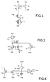
- FIG. 4 represents the polarization circuit of a detector element 1 having a sufficient impedance so that the global current id (polarization and photoelectric) which crosses it is completely injected into the channel of the "common gate" MOSFET 12 which is connected to it.
- This current not being integrated, the drain voltage of the injection transistor 12 remains almost constant during the integration period, thus making it possible to maintain constant the polarization of the detector 1 whose value, precision and stability do not depend only on the potential V ig applied to the gate of the transistor.
- an injection efficiency of 100% can be obtained using a compensated dynamic circuit, not shown here, because such a circuit makes it possible to obtain a large increase in transconductance of the MOSFET.
- input 12 by amplifying and reporting on its grid the variations in potential of the detector.
- the current i d of the detector crosses the input branch, represented by the transistor 13, of a first current mirror, of which the feedback branch, represented by the transistor 14, makes a copy of the current i d , with an amplification coefficient fixed by the ratio of the transconductances of the transistors used in each of the branches.
- FIG. 5 represents the electrical diagram of the DC component subtraction circuit.
- the output branch 14 of the first current mirror is associated in series with the output branch 15 of a second current mirror.
- This second mirror duplicates a reference current which can be generated at the periphery of the multiplexer: its input branch is symbolized in FIG. 5 by a transistor that, for the moment, will be called T x , and to which we will return later.
- This second current mirror can, like the first mirror, have an amplifier gain.
- the complementary current corresponding to the difference between the current generated i d by the detector and that taken as reference i ref is supplied by the input branch 16 of a third mirror connected to the common node of the previous two 14-15.
- the reference current i ref By adjusting, on the one hand the reference current i ref so that it is proportional to the sum of the detector bias current and the background current i bg generated by the background temperature of the scene, on the other share the amplification coefficients of the first two current mirrors 13 + 14 and 15 + Tx.
- the input branch 16 of the third mirror is crossed by a current directly proportional to the temperature differentials of the scene.
- the integrator shown in FIG. 6, consists of a capacitive element 18, or integration capacity C int , preloaded at the start of the integration period by the transistor 19 at a constant positive voltage V pst and discharged during the time by the current delivered by the output branch 17 of the third mirror.
- the integrated signal is extracted, at the end of the period, by reading the residual potential of the integration capacitor 18, by means of an amplifier 20.
- FIG. 7 gives the overall diagram of the injection circuit according to the invention, and is constituted by the connection of FIGS. 4,5 and 6.
- FIG. 8 Several variants of the invention are possible and combined in FIG. 8.
- the integration element 18 can consist of the gate of a MOS transistor 21, used as a tracking source as a output during the reading sequence, which is done by the transistor 22 connected in series with the transistor 21.
- one of the current mirrors may include several output branches mounted in parallel and separately controllable, which makes the gain of the mirror considered adjustable.
- This variant is shown on the output branch of the first mirror: transistors 14 i and 23 i .
- the transistors 13, 14 and 19 are P type MOS, the other transistors are N type, but it is understood that the technology can be adapted if this injection circuit is used for another type of as thermal imagery.
Landscapes
- Engineering & Computer Science (AREA)
- Multimedia (AREA)
- Signal Processing (AREA)
- Transforming Light Signals Into Electric Signals (AREA)
- Solid State Image Pick-Up Elements (AREA)
Applications Claiming Priority (2)
| Application Number | Priority Date | Filing Date | Title |
|---|---|---|---|
| FR9313986A FR2713037B1 (fr) | 1993-11-23 | 1993-11-23 | Circuit d'injection, en imagerie thermique. |
| FR9313986 | 1993-11-23 |
Publications (2)
| Publication Number | Publication Date |
|---|---|
| EP0654945A1 true EP0654945A1 (de) | 1995-05-24 |
| EP0654945B1 EP0654945B1 (de) | 1998-10-28 |
Family
ID=9453133
Family Applications (1)
| Application Number | Title | Priority Date | Filing Date |
|---|---|---|---|
| EP94402629A Expired - Lifetime EP0654945B1 (de) | 1993-11-23 | 1994-11-18 | Ladungseinspritzschaltung zur thermischen Abbildung |
Country Status (3)
| Country | Link |
|---|---|
| EP (1) | EP0654945B1 (de) |
| DE (1) | DE69414224D1 (de) |
| FR (1) | FR2713037B1 (de) |
Cited By (4)
| Publication number | Priority date | Publication date | Assignee | Title |
|---|---|---|---|---|
| WO1997029587A1 (en) * | 1996-02-06 | 1997-08-14 | Polaroid Corporation | Current-mediated active-pixel image sensing device with current reset |
| EP0877379A1 (de) * | 1996-02-15 | 1998-11-11 | General Electric Company | Analoge Speichereinheit |
| US7358995B2 (en) | 2002-05-30 | 2008-04-15 | Sony Corporation | Captured-image-signal processing method and apparatus and imaging apparatus |
| CN111412997A (zh) * | 2020-04-23 | 2020-07-14 | 无锡艾立德智能科技有限公司 | 一种具有像元失配校正功能的读出电路 |
Citations (9)
| Publication number | Priority date | Publication date | Assignee | Title |
|---|---|---|---|---|
| JPS56111382A (en) * | 1980-02-08 | 1981-09-03 | Hitachi Ltd | Solid image pickup apparatus |
| JPS5766324A (en) * | 1980-10-13 | 1982-04-22 | Sharp Corp | Light receiving circuit |
| FR2505589A1 (fr) * | 1981-05-09 | 1982-11-12 | Sony Corp | Appareil analyseur d'images a semi-conducteurs |
| FR2506546A1 (fr) * | 1981-05-20 | 1982-11-26 | Sony Corp | Appareil de prise de vues electronique comportant un amplificateur de sortie a commande de gain |
| JPS62171213A (ja) * | 1986-01-22 | 1987-07-28 | Nec Corp | 電流演算回路 |
| DE3625010A1 (de) * | 1986-07-24 | 1988-01-28 | Licentia Gmbh | Verfahren zur uebergabe von hintergrundsignalbefreiten nutzsignalen |
| EP0354106A1 (de) * | 1988-08-01 | 1990-02-07 | Commissariat A L'energie Atomique | Rauscheliminierende Schaltung, die in einer Festkörperbildaufnahmevorrichtung integriert ist |
| EP0521255A2 (de) * | 1991-05-02 | 1993-01-07 | Licentia Patent-Verwaltungs-GmbH | Photodetektoranordnung |
| EP0553406A1 (de) * | 1992-01-24 | 1993-08-04 | Rockwell International Corporation | Ausleseverstärker für starrende Infrarotbildebenenanlage |
-
1993
- 1993-11-23 FR FR9313986A patent/FR2713037B1/fr not_active Expired - Fee Related
-
1994
- 1994-11-18 EP EP94402629A patent/EP0654945B1/de not_active Expired - Lifetime
- 1994-11-18 DE DE69414224T patent/DE69414224D1/de not_active Expired - Lifetime
Patent Citations (9)
| Publication number | Priority date | Publication date | Assignee | Title |
|---|---|---|---|---|
| JPS56111382A (en) * | 1980-02-08 | 1981-09-03 | Hitachi Ltd | Solid image pickup apparatus |
| JPS5766324A (en) * | 1980-10-13 | 1982-04-22 | Sharp Corp | Light receiving circuit |
| FR2505589A1 (fr) * | 1981-05-09 | 1982-11-12 | Sony Corp | Appareil analyseur d'images a semi-conducteurs |
| FR2506546A1 (fr) * | 1981-05-20 | 1982-11-26 | Sony Corp | Appareil de prise de vues electronique comportant un amplificateur de sortie a commande de gain |
| JPS62171213A (ja) * | 1986-01-22 | 1987-07-28 | Nec Corp | 電流演算回路 |
| DE3625010A1 (de) * | 1986-07-24 | 1988-01-28 | Licentia Gmbh | Verfahren zur uebergabe von hintergrundsignalbefreiten nutzsignalen |
| EP0354106A1 (de) * | 1988-08-01 | 1990-02-07 | Commissariat A L'energie Atomique | Rauscheliminierende Schaltung, die in einer Festkörperbildaufnahmevorrichtung integriert ist |
| EP0521255A2 (de) * | 1991-05-02 | 1993-01-07 | Licentia Patent-Verwaltungs-GmbH | Photodetektoranordnung |
| EP0553406A1 (de) * | 1992-01-24 | 1993-08-04 | Rockwell International Corporation | Ausleseverstärker für starrende Infrarotbildebenenanlage |
Non-Patent Citations (3)
| Title |
|---|
| PATENT ABSTRACTS OF JAPAN vol. 12, no. 9 (E - 572) 12 January 1988 (1988-01-12) * |
| PATENT ABSTRACTS OF JAPAN vol. 5, no. 186 (E - 84) 25 November 1981 (1981-11-25) * |
| PATENT ABSTRACTS OF JAPAN vol. 6, no. 145 (P - 132) 4 August 1982 (1982-08-04) * |
Cited By (4)
| Publication number | Priority date | Publication date | Assignee | Title |
|---|---|---|---|---|
| WO1997029587A1 (en) * | 1996-02-06 | 1997-08-14 | Polaroid Corporation | Current-mediated active-pixel image sensing device with current reset |
| EP0877379A1 (de) * | 1996-02-15 | 1998-11-11 | General Electric Company | Analoge Speichereinheit |
| US7358995B2 (en) | 2002-05-30 | 2008-04-15 | Sony Corporation | Captured-image-signal processing method and apparatus and imaging apparatus |
| CN111412997A (zh) * | 2020-04-23 | 2020-07-14 | 无锡艾立德智能科技有限公司 | 一种具有像元失配校正功能的读出电路 |
Also Published As
| Publication number | Publication date |
|---|---|
| DE69414224D1 (de) | 1998-12-03 |
| EP0654945B1 (de) | 1998-10-28 |
| FR2713037B1 (fr) | 1995-12-29 |
| FR2713037A1 (fr) | 1995-06-02 |
Similar Documents
| Publication | Publication Date | Title |
|---|---|---|
| EP0367650B1 (de) | Photoempfindliche Vorrichtung mit Signalverstärkung im Bereich der photoempfindlichen Punkte | |
| FR2743462A1 (fr) | Dispositif de lecture de barrettes de detecteurs avec effet tdi | |
| EP0153251B1 (de) | Bildaufnahmevorrichtung mit stabförmiger multilinearer Ladungsverschiebungsanordnung | |
| FR2505589A1 (fr) | Appareil analyseur d'images a semi-conducteurs | |
| EP0749233A1 (de) | Digitalisierungsvorrichtung und -verfahren für lichtempfindliche Detektoren und Ausleseverfahren einer Matrix von Lichtdetektoren | |
| FR2924862A1 (fr) | Dispositif microelectronique photosensible avec multiplicateurs par avalanche | |
| WO2002059974A1 (fr) | Element photoelectrique a tres grande dynamique de fonctionnement | |
| EP0654945B1 (de) | Ladungseinspritzschaltung zur thermischen Abbildung | |
| EP0478457A1 (de) | Festkörperbildabtaster mit einem integrierten Störschutzfilter | |
| EP0692907B1 (de) | Schaltung zur Unterdrückung des Dunkelstromes eines Photodetektors | |
| EP0792063B1 (de) | Feld aus photoempfindlichen Sensoren | |
| EP0354106B1 (de) | Rauscheliminierende Schaltung, die in einer Festkörperbildaufnahmevorrichtung integriert ist | |
| EP2430659A1 (de) | Integrierter hochsensibler bildsensor | |
| EP0149948B1 (de) | Photoempfindliche Festkörperanordnungen | |
| EP0182679B1 (de) | Photoempfindliche Zwischenspaltanordnung mit zurückgekoppeltem Verstärker | |
| EP0207826B1 (de) | Detektorvorrichtung mit Zeitverzögerung und Integration in Phase | |
| FR2736782A1 (fr) | Dispositif et procede de lecture d'une matrice de detecteurs photoniques | |
| EP0021910A1 (de) | Durch eine Halbleitervorrichtung abgetastete Matrix strahlungsempfindlicher Detektoren und Bildaufnahmevorrichtung mit einer solchen Matrix | |
| FR2759509A1 (fr) | Circuit integrateur a linearite amelioree | |
| EP1146732B1 (de) | Photosignal-Spannungswandlerschaltung in Bildsensoren mit entfernten Integratoren | |
| EP3829160A1 (de) | Pixel mit einstellbarem dynamikbereich zur geräuschreduzierung | |
| FR2751155A1 (fr) | Dispositif de lecture pour une mosaique de detecteurs electromagnetiques, et systeme de detection equipe d'un tel dispositif | |
| FR2548499A1 (fr) | Dispositif photosensible a l'etat solide | |
| FR2813000A1 (fr) | Circuit de detection de rayonnement electromagnetique et procede de detection de rayonnement electromagnetique | |
| FR2797734A1 (fr) | Dispositif de lecture de circuits detecteurs de rayonnement agences en matrice |
Legal Events
| Date | Code | Title | Description |
|---|---|---|---|
| PUAI | Public reference made under article 153(3) epc to a published international application that has entered the european phase |
Free format text: ORIGINAL CODE: 0009012 |
|
| AK | Designated contracting states |
Kind code of ref document: A1 Designated state(s): DE FR GB IT NL |
|
| 17P | Request for examination filed |
Effective date: 19950828 |
|
| 17Q | First examination report despatched |
Effective date: 19970326 |
|
| GRAG | Despatch of communication of intention to grant |
Free format text: ORIGINAL CODE: EPIDOS AGRA |
|
| GRAG | Despatch of communication of intention to grant |
Free format text: ORIGINAL CODE: EPIDOS AGRA |
|
| GRAG | Despatch of communication of intention to grant |
Free format text: ORIGINAL CODE: EPIDOS AGRA |
|
| GRAH | Despatch of communication of intention to grant a patent |
Free format text: ORIGINAL CODE: EPIDOS IGRA |
|
| GRAH | Despatch of communication of intention to grant a patent |
Free format text: ORIGINAL CODE: EPIDOS IGRA |
|
| GRAA | (expected) grant |
Free format text: ORIGINAL CODE: 0009210 |
|
| AK | Designated contracting states |
Kind code of ref document: B1 Designated state(s): DE FR GB IT NL |
|
| PG25 | Lapsed in a contracting state [announced via postgrant information from national office to epo] |
Ref country code: NL Free format text: LAPSE BECAUSE OF FAILURE TO SUBMIT A TRANSLATION OF THE DESCRIPTION OR TO PAY THE FEE WITHIN THE PRESCRIBED TIME-LIMIT Effective date: 19981028 Ref country code: IT Free format text: LAPSE BECAUSE OF FAILURE TO SUBMIT A TRANSLATION OF THE DESCRIPTION OR TO PAY THE FEE WITHIN THE PRE;WARNING: LAPSES OF ITALIAN PATENTS WITH EFFECTIVE DATE BEFORE 2007 MAY HAVE OCCURRED AT ANY TIME BEFORE 2007. THE CORRECT EFFECTIVE DATE MAY BE DIFFERENT FROM THE ONE RECORDED.SCRIBED TIME-LIMIT Effective date: 19981028 |
|
| REF | Corresponds to: |
Ref document number: 69414224 Country of ref document: DE Date of ref document: 19981203 |
|
| GBT | Gb: translation of ep patent filed (gb section 77(6)(a)/1977) |
Effective date: 19981222 |
|
| PG25 | Lapsed in a contracting state [announced via postgrant information from national office to epo] |
Ref country code: DE Free format text: LAPSE BECAUSE OF FAILURE TO SUBMIT A TRANSLATION OF THE DESCRIPTION OR TO PAY THE FEE WITHIN THE PRESCRIBED TIME-LIMIT Effective date: 19990129 |
|
| NLV1 | Nl: lapsed or annulled due to failure to fulfill the requirements of art. 29p and 29m of the patents act | ||
| PLBE | No opposition filed within time limit |
Free format text: ORIGINAL CODE: 0009261 |
|
| STAA | Information on the status of an ep patent application or granted ep patent |
Free format text: STATUS: NO OPPOSITION FILED WITHIN TIME LIMIT |
|
| PGFP | Annual fee paid to national office [announced via postgrant information from national office to epo] |
Ref country code: GB Payment date: 19991014 Year of fee payment: 6 |
|
| 26N | No opposition filed | ||
| PGFP | Annual fee paid to national office [announced via postgrant information from national office to epo] |
Ref country code: FR Payment date: 19991123 Year of fee payment: 6 |
|
| PG25 | Lapsed in a contracting state [announced via postgrant information from national office to epo] |
Ref country code: GB Free format text: LAPSE BECAUSE OF NON-PAYMENT OF DUE FEES Effective date: 20001118 |
|
| GBPC | Gb: european patent ceased through non-payment of renewal fee |
Effective date: 20001118 |
|
| PG25 | Lapsed in a contracting state [announced via postgrant information from national office to epo] |
Ref country code: FR Free format text: LAPSE BECAUSE OF NON-PAYMENT OF DUE FEES Effective date: 20010731 |
|
| REG | Reference to a national code |
Ref country code: FR Ref legal event code: ST |