EP0654948A2 - Méthode et appareil de traitement d'images - Google Patents
Méthode et appareil de traitement d'images Download PDFInfo
- Publication number
- EP0654948A2 EP0654948A2 EP94308500A EP94308500A EP0654948A2 EP 0654948 A2 EP0654948 A2 EP 0654948A2 EP 94308500 A EP94308500 A EP 94308500A EP 94308500 A EP94308500 A EP 94308500A EP 0654948 A2 EP0654948 A2 EP 0654948A2
- Authority
- EP
- European Patent Office
- Prior art keywords
- threshold value
- image data
- value
- data
- quantizing
- Prior art date
- Legal status (The legal status is an assumption and is not a legal conclusion. Google has not performed a legal analysis and makes no representation as to the accuracy of the status listed.)
- Granted
Links
Images








Classifications
-
- H—ELECTRICITY
- H04—ELECTRIC COMMUNICATION TECHNIQUE
- H04N—PICTORIAL COMMUNICATION, e.g. TELEVISION
- H04N19/00—Methods or arrangements for coding, decoding, compressing or decompressing digital video signals
- H04N19/90—Methods or arrangements for coding, decoding, compressing or decompressing digital video signals using coding techniques not provided for in groups H04N19/10-H04N19/85, e.g. fractals
-
- H—ELECTRICITY
- H04—ELECTRIC COMMUNICATION TECHNIQUE
- H04N—PICTORIAL COMMUNICATION, e.g. TELEVISION
- H04N5/00—Details of television systems
- H04N5/14—Picture signal circuitry for video frequency region
- H04N5/20—Circuitry for controlling amplitude response
- H04N5/202—Gamma control
-
- H—ELECTRICITY
- H04—ELECTRIC COMMUNICATION TECHNIQUE
- H04N—PICTORIAL COMMUNICATION, e.g. TELEVISION
- H04N5/00—Details of television systems
- H04N5/66—Transforming electric information into light information
- H04N5/70—Circuit details for electroluminescent devices
Definitions
- the invention relates to image processing method and apparatus for inputting digital image data and converting to image data whose number of bits is smaller than that of the input data and, more particularly, to image processing method and apparatus for enabling a half tone image to be displayed for a display using, for example, a ferroelectric liquid crystal and having a gradation expressing ability of a small number of gradations such as two values, four values, or the like.
- a ferroelectric liquid crystal (hereinafter, simply referred to as an FLC) display among liquid crystal displays has a feature such that the liquid crystal has a "memory performance" to hold a display state changed by applying an electric field, so that a contrast is not deteriorated even if the number of scan lines increases. Therefore, an attention is paid to the FLC display as a device which can display by a large screen and at a high precision even in a simple matrix structure.
- the FLC fundamentally can express only two gradations by one element. Even in case of displaying one pixel by a plurality of elements, the number of gradations which can be expressed is four values, six values, eight values, or the like and its gradation expressing ability is low.
- a half tone process such as dither method, error diffusion method, or the like has been used as a method of improving the gradation expressing ability of a display device of a low gradation expressing ability.
- Such half tone processing methods have already widely been used in a printer apparatus of a binary output and the like.
- an output value is decided by comparing an input value and a predetermined threshold value, by changing the threshold value in a predetermined area, a half tone is expressed in the predetermined area in a macro manner.
- a multivalue dither in which the dither process is executed to a device of a multivalue output, a case where a 4-level dither process by a (2 x 2) dither matrix is executed to input data of eight bits and a 4-level output of 0 to 3 is obtained will now be described with reference to the drawings.
- the 4-level dither of the (2 x 2) dither matrix four threshold tables each having three threshold values as shown in Fig.
- dither matrix 2 are used in correspondence to cells of a dither matrix as shown in Fig. 3.
- the dither matrix is moved and applied to each pixel in the image data at a period of two pixels in both of the vertical and horizontal directions.
- the corresponding pixel data is compared with a proper one of the threshold tables, and either one of the four values which can be outputted by the device is selected and outputted. For example, assuming that the input data is 100 and the pixel position corresponds to the position of the dither matrix 1 in Fig. 3, a threshold table 1 is applied. In this case, since 100 is larger than the second small-threshold value 95 in a threshold table 1, an output value is set to 2.
- a threshold table 2 is selected. Even when the input value is equal to 100, since it is smaller than a threshold value 117, the output value is set to 1. In the case where the pixel positions correspond to the positions of 3 and 4 of the dither matrix, the output values are also set to 1. In such an area of (2 x 2), a combination of outputs of 2/1/1/1 is obtained and a half tone of 1.25 is expressed as a whole matrix. By also executing similar processes to the other input values, a correspondence relation of the input value/output value as shown in Fig. 2 is obtained every pixel position. A half tone can be falsely obtained as a combination of them.
- Another concern of the invention is to provide image processing method and apparatus which can suppress the generation of scintillation noises when data of one pixel is quantized to multivalue data of at least a 3-level or higher by using a plurality of threshold values.
- An embodiment of the invention provides an image processing method and apparatus in which when data of one pixel is quantized to multivalue data by using a plurality of threshold values, by providing an upper threshold value and a lower threshold value for all of the threshold values, the generation of scintillation noises having a possibility such that they are generated near all of the threshold values can be suppressed.
- a further embodiment of the invention provides an image processing method and apparatus which can accomplish both of the reduction of scintillation noises and the high picture quality by changing a deviation amount from a standard threshold value for each of a plurality of threshold values.
- Fig. 1 is a block diagram showing a construction of an image processing system (hereinafter, also simply referred to as a system) according to a typical embodiment of the invention.
- an analog moving image signal which was raster framed is inputted and converted to digital data of eight bits by an A/D converter 101.
- the produced multivalue digital image signal (I i ) of eight bits is quantized to the data of, for example, two bits by a multivalue dither method by an image processing apparatus 102.
- the quantized image data obtained is stored into a quantization frame buffer 103.
- the quantized image data is read out by a display control apparatus 104 and is displayed by a display 105 such as an FLC display or the like. Such a series of operations are executed for the image data input in a real-time manner.
- the analog moving image signal which is inputted to the system includes noises which are mixed to a transfer system (not shown). Even in an A/D converting process in the A/D converter 101, a conversion error occurs by an incomplete waveform which is peculiar to the analog signal. Therefore, the digital image signal which is inputted to the image processing apparatus 102 has noise components for the inherent digital data produced on the transmission side of the analog image signal. In the system, it is assumed that such a noise component has a small amount such that it can be statistically handled by numerical values like a standard deviation.
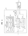
- Fig. 4 is a block diagram showing a detailed construction of the image processing apparatus 102. The construction and operation of the image processing apparatus 102 will now be described hereinbelow with reference to Fig. 4.
- Reference numeral 301 denotes a threshold memory to store a plurality of threshold tables for the dither process.
- the threshold memory 301 stores a standard threshold table (ItcTab) 302, an upper threshold table (IthTab) 304, and a lower threshold table (ItlTab) 305.
- the upper threshold table 304 and lower threshold table 305 are together called a deviation threshold table 303.
- Deviation threshold values which are independent every threshold value can be set into the upper threshold table (IthTab) 304 and lower threshold table (ItlTab) 305, respectively.
- a value based on a standard deviation of an amplitude of noises included in the digital image signal (I i ) is uniformly set as a deviation threshold value. For example, when explaining the threshold table 1 shown in Fig.
- a threshold selector 308 receives the digital moving image signal (I i ) and quantized (dither processed) data (Q prev ) of one-previous frame corresponding to the same position as that of the pixel that is at present being processed from the quantization frame buffer 103.
- the most proper threshold table is selected from a plurality of threshold tables held in the threshold memory 301 and is supplied to a dither processor 309.
- the quantized data Q has a value converted to eight bits in accordance with the input data. For example, in case of converting the data to the 4-level data, the quantization results are (0, 1, 2, 3). However, in case of eight bits, they are set to (0, 85, 170, 255), respectively.
- the dither processor 309 inputs the digital image signal (I i ) and compares with a threshold table (I t ) which is supplied from the threshold selector 308, thereby converting to data (Q cur ) whose number of bits is smaller than the number of bits to express a pixel that is shown by the digital image signal (I i ).
- the data (Q cur ) is stored to the position corresponding to the quantization frame buffer 103.
- a timer 306 detects the elapse of predetermined time and sends a detection signal to the threshold selector 308.
- the threshold selector 308 executes a threshold table selecting process in response to the reception of a detection signal and resets the timer 306 at the same time.
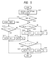
- the dither process in the image processing apparatus 102 will now be described with reference to a flowchart shown in Fig. 5.
- the flowchart is executed by a control unit (not shown). Particularly, processes of the threshold selector 308 and dither processor 309 are explained.
- the quantized data Q k is converted to eight bits, it becomes I0, I1, ..., I k , I k+1 , ..., I N .
- N 2
- the quantized data has four values of Q0, Q1, Q2, and Q3.
- the value of k satisfying I k ⁇ I i ⁇ I k+1 is obtained.
- a standard threshold value (I ntc ) to be compared in the multivalue dither process is determined on the basis of the value of k.
- step S402 a check is made to see if a time-out detection signal has been generated from the timer 306 or not. When such a signal is not detected, the processing routine advances to step S403. When the signal is detected, step S409 follows.
- step S403 the quantized data (Q prev ) of the previous frame corresponding to the pixel position of the pixel that is at present being processed is read out from the quantization frame buffer 103 and is compared with the standard threshold value (I ntc ).
- quantization data (Q prev ) which is used here, the data converted to eight bits is also used.
- step S404 When Q prev > I ntc , the processing routine advances to step S404.
- a lower threshold value (I ntl ) is used as a threshold value (I t ).
- the processing routine advances to step S405 and the upper threshold value (I nth ) is used as a threshold value (I t ).
- the threshold value (I t ) decided by the processes in steps S403 to S405 is supplied to the dither processor 309 irrespective of the results of the above processes. Thus, the threshold value that is actually used is selected in the dither processor 309.
- the dither processor 309 executes the dither process by using the threshold value (I t ) which is selected and outputted by the threshold selector 308 and the input digital image signal (I i ).
- step S406 the magnitude relation between I t and I i is examined in step S406.
- the processing routine advances to step S407 and the quantized data (I k+l ) is selected.
- step S408 follows and the quantized data (I k ) is selected.
- step S402 when the time-out is detected in step S402, the processing routine advances to step S409 and the timer 306 is reset.
- steps S410 to S412 the dither processor 309 subsequently executes the dither process by using the standard threshold value (I ntc ) and input digital image signal (I i ).
- step S410 the magnitude relation between I ntc and I i is examined in step S410.
- step S411 follows and the quantized data (I k+l ) is selected.
- I i ⁇ I ntc the processing routine advances to step S412 and the quantized data (I k ) is selected.
- the upper threshold value (I nth ) and lower threshold value (I ntl ) having the deviations of ⁇ h and ⁇ l are set.
- the threshold value is set to I ntl and whether I i > I ntl or not is discriminated by the dither processor 309.
- the threshold value can be properly shifted on the basis of the dither processing result of the previous frame.
- the input signal which oscillates at positions near the threshold value so long as its amplitude doesn't exceed (
- the output is fixed to either one of I k and I k+l .
- a state in which the dither processing result oscillates between both of I k and I k+l due to an influence by the noises can be suppressed in spite of the fact that the input data is equal.
- the data of one pixel is quantized to the multivalue data by using a plurality of threshold values and by providing the upper threshold value and lower threshold value for all of the threshold values, the generation of the scintillation noises can be suppressed.
- the dither process is executed by using the standard threshold value every predetermined time, so that the deterioration of the picture quality can be suppressed.
- the first moving picture image data of n gradations per each pixel is inputted and converted into the second moving picture image data of a smaller number of gradations
- the first moving picture image data is compared with the second moving picture image data which is one-frame previous and corresponds to the pixel position of the first moving picture image data.
- a microamount is dynamically changed for the threshold value selected for the above conversion and the conversion result can be obtained in consideration of the continuity of the data between frames.
- the conversion of the input and output characteristics according to the display characteristics of the display namely, what is called a gamma converting process is ordinarily necessary for the input image data.
- Fig. 7 is a block diagram showing a construction of an image display system in the second embodiment of the invention.
- the analog moving image signal which was raster framed is inputted and converted to the digital data of eight bits by an A/D converter 201.
- Gamma characteristics which the CRT has are added to the produced digital image signal by a gamma characteristic addition circuit 202 (which will be explained in detail hereinlater).
- the image signal is quantized to the data of, for instance, two bits by the dither process by an image processing apparatus 203.
- the quantized image data derived is stored into a quantization frame buffer 204.
- the data is read out at any time by a display control apparatus 205 and is displayed to a display 206.
- the above series of operations are executed to the image data input in a real-time manner.
- the analog moving image signal which is inputted to the system includes noises which come from the outside and are mixed to a transfer system.
- a conversion error due to incompleteness of a waveform which is peculiar to the analog signal occurs in the A/D converting process by the A/D converter 201.
- the digital image signal which is supplied to the image processing apparatus 203 has a noise component for the inherent digital data existing on the feeding side of the analog image signal. In the system, however, such a noise component can be statistically handled by numerical values like a standard deviation.
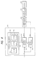
- a threshold memory 701 comprises a plurality of threshold tables.
- the threshold memory 701 has a standard threshold table (ItcTab) 702, an upper threshold table (IthTab) 704, and a lower threshold table (ItlTab) 705.
- the upper threshold table 704 and lower threshold table 705 are together called a deviation threshold table 703. Values which are vertically deviated from a threshold value set in the standard threshold table 702 by only ⁇ h and ⁇ l are held in the deviation threshold table 703, respectively.
- ⁇ h and ⁇ l can have values every threshold value.
- a threshold selector 707 inputs the digital moving image signal I i sent from the gamma characteristic addition circuit 202 and inputs the previous-frame data Q prev at the pixel position of the pixel which is at present being processed in the quantization frame buffer 204.
- a proper threshold value is selected from a plurality of threshold values held in the threshold memory and is supplied to a dither processor 708. A selecting method of the threshold value will be described hereinlater.
- the dither processor 708 inputs the digital image signal I i and compares with the threshold value which is supplied from the threshold selector 707, thereby converting to the data whose number of bits is smaller than that of I i and storing it to the position of the pixel under processing in the quantization frame buffer 204.
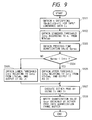
- Fig. 9 is a flowchart for explaining a process in the threshold selector 707 and a process in the dither processor 708 subsequent to it.
- N 2
- a value of (n) satisfying Q n ⁇ I ⁇ Q n+1 is obtained.
- the threshold value I ntc according to the value of (n) is obtained from the standard threshold table (ItcTab) 702.
- the quantized data Q prev of the previous frame corresponding to the pixel position of the pixel which is at present being processed is read out from the quantization frame buffer 204.
- the magnitudes are compared between Q prev and I ntc .
- the dither processor 708 executes the dither process as shown in step S507 by using I t which is selected and outputted by the threshold selector 707 and the input digital image signal I i .
- the dither processor 708 writes the output value Q cur obtained as a result of the dither process to the present pixel position in the quantization frame buffer 204.
- the CRT has nonlinear input/luminance characteristics called gamma characteristics.
- the gamma characteristic addition circuit 202 as shown in Fig. 7 is provided for the display interface of the embodiment.
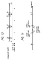
- the gamma characteristic addition circuit 202 adds characteristics as shown in Fig. 10A to the digital input image signal from the A/D converter 101. In this instance, similar characteristics as shown in Fig. 10B are also added to the noises. At this time, as shown in Fig. 11, the amplitude of noises is reduced in an area in which the inclination of the curve of the gamma characteristic is smaller than 1. However, in an area where the inclination is larger than 1, a phenomenon such that the amplitude of noises is contrarily increased occurs.
- the set deviation increases to a value larger than it is needed in the area where the inclination of the gamma characteristic curve is smaller than 1, so that the picture quality is deteriorated.
- the deviation is not enough large.
- the influence by the noises cannot be absorbed by the deviation of the threshold value and the scintillation noises are generated.
- the value (3 ⁇ ) that is about three times as large as the distribution of the noise component of the signal after completion of the A/D conversion in each standard threshold is set to the deviation of the upper threshold value and the deviation of the lower threshold value, respectively.
- the inclination of the gamma characteristic curve which is given by the gamma characteristic addition circuit 202 is obtained in each standard threshold value.
- the inclination is multiplied with the deviation of the upper threshold value and the deviation of the lower threshold value which were obtained before.
- the resultant values are further added to the standard threshold value.
- the resultant addition values are set to the upper threshold value and lower threshold value, respectively.
- Fig. 12 shows the measurement result of the data which is outputted from the A/D converter when a value of a certain standard threshold value is written as an "original luminance" into a VRAM of the computer.
- Fig. 13 shows the upper and lower threshold values for the standard threshold value shown in the threshold table 1 in Fig. 2. As will be obviously understood from Fig. 13, as the value of the standard threshold value is large, the deviation amount is set to a large value.
- the threshold values which are deviated from the standard threshold value which has inherently been optimized are used, so that the picture quality is slightly deteriorated. Therefore, it is desirable to minimize the deviations of the upper and lower threshold values from the standard threshold value.
- the deviations are set to be too small, the inherent effect of the hysteresis dither is extinguished and the scintillation noises are generated.
- timer 306 shown in Fig. 4 in the first embodiment is not provided in Fig. 8 of the second embodiment, it is also possible in the second embodiment to provide the timer in a manner similar to the first embodiment and to execute the dither process by using the standard threshold value every predetermined time.
- the threshold table memory in Fig. 8 includes the standard threshold table 702, upper threshold table 704, and lower threshold table 705.
- an upper threshold deviation table and lower threshold deviation table in which only deviation amounts from the standard threshold value have been stored can be also used in place of the upper threshold table 704 and lower threshold table 705.
- the memory capacity of the threshold table memory 701 can be reduced.
- the threshold selector 707 adds the value of the deviation selected in step S505 or S506 in Fig. 9 to the standard threshold value associated with I i at the same time.
- the setting of each value of the upper and lower threshold deviations in this case can be executed in a manner similar to the case described in the above second embodiment.
- a hysteresis dither as a base is realized by the following algorithm.
- upper and lower threshold values having deviations of ⁇ ln and ⁇ hn in the upper/lower directions of the standard threshold value are preset, respectively.
- two adjacent luminances Q n and Q n+1 which can be displayed and which sandwich the input luminance value I i are examined, thereby obtaining the value of (n).
- the upper threshold value I ntu and lower threshold value I ntl existing between the above two displayable luminances are obtained.
- step S603 a check is made to see if the input luminance value I i exists between I ntu and I ntl or not. When it exists between them, the output value Q prev at the same pixel position of the previous frame is obtained from the quantization frame buffer 204 and is outputted as an output value in the present frame. When the input luminance doesn't exist between I ntu and I ntl , the upper threshold value I ntu is used as a threshold value and the dither process is executed. Finally, the output value Q cur is written at the present pixel position in the quantization frame buffer 204.
- the above series of algorithms eventually output the same value as that of the algorithm shown in Fig. 9.
- the setting of each value of the upper and lower threshold deviations in case of using the algorithm shown in Fig. 15 can be also executed in a manner similar to that described in the above second embodiment.
- Fig. 16 is a block diagram showing a construction of an image display system according to the third embodiment of the invention.
- reference numeral 811 denotes a CPU for controlling the whole apparatus; 812 a main memory which is used to store programs which are executed by the CPU 811 and is used as a work area when the program is executed; 813 an input/output control apparatus (I/O controller) having an interface such as an RS-232C and the like; 814 a keyboard to input character information and control information from the user; 815 a mouse as a pointing device; 816 a graphic card for storing display data and for transferring a display signal to a display apparatus; 817 a disk interface for controlling a hard disk drive (HDD) 818 and a floppy disk drive (FDD) 819 as external memory apparatuses; and 820 a bus system comprising a data bus, a control bus, and an address bus for connecting signals among the above component elements.
- a video memory 821 and an RAMDAC 822 are built in the graphic card
- Reference numeral 830 denotes a ferroelectric liquid crystal display (hereinafter, simply referred to as an FLCD).
- the FLCD 830 comprises an FLC display panel 834 in which matrix-like electrodes are arranged and a ferroelectric liquid crystal is sealed in two glass plates which were subjected to an orientating process; an information electrode driver IC 832; a scan electrode driver IC 833; and a panel controller 831 to control the panel driving.
- Information electrodes and scan electrodes of the FLC panel 834 are connected to the information electrode driver IC 832 and scan electrode driver IC 833, respectively.
- Reference numeral 840 denotes a ferroelectric liquid crystal display interface (hereinafter, simply referred to as an FLCD interface) having the image processing apparatus of the invention.
- the FLCD 830 which is used in the embodiment is a monochromatic (two or four gradations) display having a panel size of 15 inches and a resolution of [1280 dots (in the horizontal direction) x 1024 (in the vertical direction) lines].
- Fig. 17 is a block diagram showing a construction of the FLCD interface 840.
- reference numeral 841 denotes an A/D converter for converting luminance information of each pixel which is sent as an analog signal from the graphic card 816 to digital signal; 842 an image processing unit; 843 a frame buffer to store the image processing result of one frame; 844 an output controller for transferring data in the frame buffer 843 to the FLCD 830.
- the image processing unit 842 comprises an image processing controller 845, a dither processing circuit 846, and an output change-over switch 847.
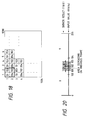
- Fig. 18 is a diagram showing a dither matrix of (2 x 2) pixels which is used by the dither processing circuit 846.
- the dither processing circuit 846 compares a luminance of each of the inputted pixels and threshold values of the dither matrix, thereby obtaining an output value. For example, the luminance of the pixel (1, 1) at the left upper edge is compared with a threshold value "51". When the luminance is smaller than "51”, "0" is generated. When it is equal to or larger than "51”, "1" is outputted.
- the luminance of the pixel (2, 1) is compared with a threshold value "153"
- the luminance of the pixel (1, 2) is compared with a threshold value "204”
- the luminance of the pixel (2, 2) is compared with a threshold value "102”, respectively.
- the same dither matrix is always used for each frame. Therefore, the threshold value of the pixel (1, 1) is always set to "51".
- the image processing controller 845 controls an output from the output change-over switch 847 by using the luminance value of each pixel which is inputted to the dither processing circuit 846 and the processing result of the previous frame of such a pixel which was read out from the frame buffer 843 as parameters.
- the result stored in the frame buffer 843 is not always the result of the previous frame but there is a case where it becomes the result of the two- or three-previous frame.
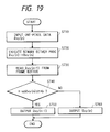
- step S710 data of one pixel [l xy (n) n denotes the number of frames and x, y indicate a coordinate value in the horizontal (x) direction and a coordinate value in the vertical (y) direction which two-dimensionally determine an address in the frame memory] is inputted.
- step S720 the binary dither process of (2 x 2) pixels is executed as mentioned above, thereby converting l xy (n) to an output value [D xy (n)].
- Dither data [D xy (n-1)] at the same position before one frame which was outputted to the frame buffer 843 by the dither process as mentioned above is read out from the frame buffer 843 in step S730.
- the output value [D xy (n)] is set to "0" or "1".
- step S740 the image processing controller 845 discriminates whether the luminance [l xy (n)] of a certain pixel inputted is close to a threshold value (t) of such a pixel or not. It is judged that the luminance is near the threshold value in the case where the input value [l xy (n)] satisfies the following condition: (t - a) ⁇ input value [l xy (n)] ⁇ (t + b) where, a, b (constant) ⁇ 0.
- the values of (a) and (b) are decided in consideration of an inter-frame fluctuation width of the luminance which is caused when performing the analog/digital conversion and are set to values which are equal to or larger than such a fluctuation width.
- step S740 when it is judged that the input value is near the threshold value, the processing routine advances to step S750.
- the output change-over switch 847 is controlled and D xy (n-1) is set to a dither output of the pixel.
- step S760 When it is judged that the input value is not close to the threshold value, the processing routine advances to step S760.
- the output change-over switch 847 is controlled and D xy (n) is set to a dither output of the pixel.
- the image processing controller 845 sets the processing result [D xy (n)] of the dither processing circuit 846 to the output value. Namely, when l xy (n) ⁇ 101, the output value [D xy (n)] is set to "0". When l xy (n) > 103, the output value is set to "1". When l xy (n) is close to the threshold value (t), the image processing controller 845 sets the result of the same pixel which was read out from the frame buffer 843 is set to the output value.
- Such an operation is executed for every frame and every pixel.
- the processing result D xy (n) of the dither processing circuit 846 is unconditionally set to the output value.
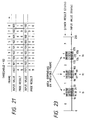
- Fig. 21 is a diagram showing an output value for every frame in the case where the input luminance value fluctuates within a range of +1 around 102 and 101 as centers, respectively.
- the threshold value is set to "102" here.
- a processing result A shows the case where the process was performed in accordance with the conventional dither method.
- a processing result B shows the case where the foregoing process was executed.
- the output value of the image process becomes constant at least after two frames.
- the dither processing circuit 846 executes the 4-level dither process of (2 x 2) pixels by using the threshold table shown in Fig. 2.
- the dither processing circuit 845 compares the luminance value [input value: l xy (n)] of the pixel (1, 1) at the left upper edge with three threshold values "10", “95”, and "180” by using, for example, the threshold table 1 shown in Fig. 2.
- the output value [D xy (n)] which is obtained by the comparison is as follows.
- the luminance value of the pixel (2, 1) is compared with threshold values "32", “117", and “202".
- the luminance of the pixel (1, 2) is compared with threshold values "53", “138", and “223” by using the threshold table 3 shown in Fig. 2.
- the luminance of the pixel (2, 2) is compared with threshold values "74", "159", and "244" by using the threshold table 4 shown in Fig. 2.
- the image processing controller 845 controls the output from the output change-over switch 847 by using the luminance value of each pixel which is inputted to the dither processing circuit 846 and the processing result of the previous frame of such a pixel which was read out from the frame buffer 843 as parameters.
- step S710 the 4-level dither process of (2 x 2) pixels is executed as mentioned above in step S725 and l xy (n) is converted to the output value [D xy (n)].
- (a to f) denote constants of 0 or more.
- the values of (a to f) are determined to values which are equal to or larger than the fluctuation width.
- the inter-frame fluctuation width lies within a range of ⁇ 1 in all of the luminances and that all of the values of (a to f) are set to "1".
- step S741 to S746 the processing routine advances to step S50 and D xy (n) is set to the dither output of such a pixel.
- step S741 to S746 when it is judged that the input value is close to the threshold values, the processing routine advances to steps S742, S744, and S746. A check is further made to see if the result [D xy (n-1)] of the same pixel of the previous frame which was read out from the frame buffer is equal to the value which can be used as an output value near the threshold value or not.
- the processing result [D xy (n)] of the dither processing circuit 46 is set to the-output value.
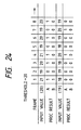
- Fig. 24 shows an output value for every frame in the case where the input luminance value fluctuates within a range of ⁇ 1 around 20 and 19 as centers, respectively.
- the processing result A shows the case where the process was executed in accordance with the conventional dither process.
- the processing result B shows the case where the foregoing process was performed.
- the output value of the image process is set to be constant after two frames in a manner similar to the above.
- the dither processing result of the present frame is determined with reference to the dither processing result at the same position of one frame before. Therefore, the fluctuation of the inter-frame luminance value doesn't directly appear in the display output.
- the display picture quality can be improved.
- the display system shown in the third embodiment uses the display panels of monochromatic two gradations and four gradations of the FLCD, the invention is not limited to such panels. For example, even in case of a system using a color panel in which one pixel is RRGGBB (6 bits/pixel) as an FLC panel, a similar result is obtained.
- a check is made to see if the value of the inputted multivalue image data lies within a range near a predetermined threshold value or not. Either one of the mode in which the image data which has already been converted and stored is set to the image processing result and the mode in which the image data converted by the converting means is set to the image processing result is selected in accordance with the result of the discrimination. Therefore, when the above image processing result is outputted to, for example, the image processing display system which handles data such that the image data value of each pixel fluctuates every input frame, its output value becomes stable. Therefore, there is an effect such that a phenomenon (sparkling noises) such that many points of the display screen flicker and the picture quality is deteriorated in spite of the fact that the image is in a stationary state can be prevented.
- sparkling noises such that many points of the display screen flicker and the picture quality is deteriorated in spite of the fact that the image is in a stationary state can be prevented.
- the invention can be also applied to a system comprising a plurality of apparatuses or to an apparatus comprising only one apparatus.
- the invention can be also obviously applied to the case where the invention is accomplished by supplying a program to a system or an apparatus.
Landscapes
- Engineering & Computer Science (AREA)
- Multimedia (AREA)
- Signal Processing (AREA)
- Image Processing (AREA)
- Facsimile Image Signal Circuits (AREA)
Applications Claiming Priority (6)
| Application Number | Priority Date | Filing Date | Title |
|---|---|---|---|
| JP28896393A JP3313852B2 (ja) | 1993-11-18 | 1993-11-18 | 画像処理装置 |
| JP288963/93 | 1993-11-18 | ||
| JP288964/93 | 1993-11-18 | ||
| JP28896493 | 1993-11-18 | ||
| JP28896393 | 1993-11-18 | ||
| JP28896493 | 1993-11-18 |
Publications (3)
| Publication Number | Publication Date |
|---|---|
| EP0654948A2 true EP0654948A2 (fr) | 1995-05-24 |
| EP0654948A3 EP0654948A3 (fr) | 1996-02-07 |
| EP0654948B1 EP0654948B1 (fr) | 2004-08-25 |
Family
ID=26557403
Family Applications (1)
| Application Number | Title | Priority Date | Filing Date |
|---|---|---|---|
| EP94308500A Expired - Lifetime EP0654948B1 (fr) | 1993-11-18 | 1994-11-17 | Méthode et appareil de traitement d'images |
Country Status (3)
| Country | Link |
|---|---|
| US (1) | US5909512A (fr) |
| EP (1) | EP0654948B1 (fr) |
| DE (1) | DE69433963T2 (fr) |
Families Citing this family (12)
| Publication number | Priority date | Publication date | Assignee | Title |
|---|---|---|---|---|
| JPH10313407A (ja) * | 1997-05-12 | 1998-11-24 | Riso Kagaku Corp | 画像処理装置 |
| JP3576810B2 (ja) * | 1998-05-28 | 2004-10-13 | シャープ株式会社 | 画像処理装置 |
| US6724437B2 (en) * | 1998-06-17 | 2004-04-20 | Koninklijke Philips Electronics N.V. | Method and device for adding noise to a video signal for improving a display of the video signal |
| US6906825B1 (en) * | 1999-06-14 | 2005-06-14 | Toshiba Tec Kabushiki Kaisha | Image processor and color image processor |
| JP4371566B2 (ja) * | 2000-11-22 | 2009-11-25 | キヤノン株式会社 | 色処理装置およびその方法 |
| JP2002185974A (ja) * | 2000-12-12 | 2002-06-28 | Canon Inc | 画像処理装置およびその方法 |
| US20020154137A1 (en) * | 2001-02-21 | 2002-10-24 | See-Rt Technology Ltd. | Transmission of digital data from a screen |
| US7558412B2 (en) * | 2004-02-06 | 2009-07-07 | General Electric Company | System and method for compensation of scintillator hysteresis in x-ray detectors |
| JP4581927B2 (ja) * | 2005-09-07 | 2010-11-17 | セイコーエプソン株式会社 | 表示装置のぎらつき測定方法およびぎらつき測定装置 |
| US8649915B2 (en) * | 2010-05-28 | 2014-02-11 | The Clear View Group Llc | Method and apparatus to facilitate providing a synthetic view of terrain for use in a moving vehicle |
| CN107646132B (zh) | 2015-04-27 | 2021-02-12 | 伊英克公司 | 用于驱动显示系统的方法和设备 |
| CN106991972B (zh) * | 2017-05-02 | 2019-05-03 | 深圳市华星光电半导体显示技术有限公司 | 一种有机发光面板的开机亮度控制方法 |
Family Cites Families (9)
| Publication number | Priority date | Publication date | Assignee | Title |
|---|---|---|---|---|
| GB1218015A (en) * | 1967-03-13 | 1971-01-06 | Nat Res Dev | Improvements in or relating to systems for transmitting television signals |
| US3959583A (en) * | 1975-01-21 | 1976-05-25 | Bell Telephone Laboratories, Incorporated | Animated dithered display systems |
| US3997719A (en) * | 1975-03-19 | 1976-12-14 | Bell Telephone Laboratories, Incorporated | Bi-level display systems |
| US4268861A (en) * | 1978-09-18 | 1981-05-19 | Massachusetts Institute Of Technology | Image coding |
| US4531160A (en) * | 1983-05-03 | 1985-07-23 | Itek Corporation | Display processor system and method |
| JPH0242873A (ja) * | 1988-02-18 | 1990-02-13 | Matsushita Graphic Commun Syst Inc | 画像信号処理方法および画像信号処理装置 |
| US5185602A (en) * | 1989-04-10 | 1993-02-09 | Cirrus Logic, Inc. | Method and apparatus for producing perception of high quality grayscale shading on digitally commanded displays |
| JPH03141768A (ja) * | 1989-10-27 | 1991-06-17 | Canon Inc | 画像形成装置 |
| US5272469A (en) * | 1991-07-01 | 1993-12-21 | Ncr Corporation | Process for mapping high resolution data into a lower resolution depiction |
-
1994
- 1994-11-16 US US08/341,065 patent/US5909512A/en not_active Expired - Fee Related
- 1994-11-17 EP EP94308500A patent/EP0654948B1/fr not_active Expired - Lifetime
- 1994-11-17 DE DE69433963T patent/DE69433963T2/de not_active Expired - Lifetime
Also Published As
| Publication number | Publication date |
|---|---|
| DE69433963D1 (de) | 2004-09-30 |
| EP0654948B1 (fr) | 2004-08-25 |
| US5909512A (en) | 1999-06-01 |
| DE69433963T2 (de) | 2005-09-08 |
| EP0654948A3 (fr) | 1996-02-07 |
Similar Documents
| Publication | Publication Date | Title |
|---|---|---|
| EP0583102B1 (fr) | Dispositif de contrÔle pour dispositif d'affichage | |
| US5909512A (en) | Method and apparatus to reduce scintillation in dithered display systems | |
| US7002594B2 (en) | Image processing apparatus and image display apparatus using same | |
| EP0573174A1 (fr) | Méthode et dispositif de commande d'affichage | |
| US7202879B2 (en) | Image processing method, image processing apparatus, electronic device, image processing program, and recording medium on which the same program is recorded | |
| US6587120B2 (en) | Liquid crystal display system capable of reducing and enlarging resolution of input display data | |
| US5739808A (en) | Display control method and apparatus | |
| KR100825339B1 (ko) | 화상처리회로 및 화상처리방법 | |
| US5379051A (en) | Method and apparatus for rearranging and displaying line data | |
| CN115841796B (zh) | 显示面板的控制方法、装置及显示装置 | |
| JP3171993B2 (ja) | 画像処理方法及び装置 | |
| JP2000338922A (ja) | 映像処理装置 | |
| KR20070012215A (ko) | 화상처리회로 | |
| JPH06332395A (ja) | 画像処理方法及び装置 | |
| JP3311175B2 (ja) | 画像処理方法及びその装置 | |
| EP0571878B1 (fr) | Méthode et dispositif de commande d'affichage | |
| JP3313852B2 (ja) | 画像処理装置 | |
| JP3209379B2 (ja) | 画像処理装置及びその方法 | |
| KR20080066288A (ko) | 영상표시장치 및 그 영상표시방법 | |
| JPH05108026A (ja) | 多階調表示装置 | |
| JPH1152919A (ja) | 単純マトリクス型液晶表示装置 | |
| JPH06222740A (ja) | 液晶表示装置 | |
| Sasaki et al. | P‐55: Tiny Codec for Decreasing Frame Memories in Display Driver ICs—Smart Pixel‐Data Codec (SPC) | |
| JPH06266317A (ja) | 表示装置 | |
| JPH0980380A (ja) | 液晶表示装置 |
Legal Events
| Date | Code | Title | Description |
|---|---|---|---|
| PUAI | Public reference made under article 153(3) epc to a published international application that has entered the european phase |
Free format text: ORIGINAL CODE: 0009012 |
|
| AK | Designated contracting states |
Kind code of ref document: A2 Designated state(s): DE ES FR GB IT NL SE |
|
| PUAL | Search report despatched |
Free format text: ORIGINAL CODE: 0009013 |
|
| AK | Designated contracting states |
Kind code of ref document: A3 Designated state(s): DE ES FR GB IT NL SE |
|
| 17P | Request for examination filed |
Effective date: 19960619 |
|
| 17Q | First examination report despatched |
Effective date: 19980416 |
|
| GRAP | Despatch of communication of intention to grant a patent |
Free format text: ORIGINAL CODE: EPIDOSNIGR1 |
|
| GRAS | Grant fee paid |
Free format text: ORIGINAL CODE: EPIDOSNIGR3 |
|
| GRAA | (expected) grant |
Free format text: ORIGINAL CODE: 0009210 |
|
| AK | Designated contracting states |
Kind code of ref document: B1 Designated state(s): DE ES FR GB IT NL SE |
|
| PG25 | Lapsed in a contracting state [announced via postgrant information from national office to epo] |
Ref country code: NL Free format text: LAPSE BECAUSE OF FAILURE TO SUBMIT A TRANSLATION OF THE DESCRIPTION OR TO PAY THE FEE WITHIN THE PRESCRIBED TIME-LIMIT Effective date: 20040825 Ref country code: IT Free format text: LAPSE BECAUSE OF FAILURE TO SUBMIT A TRANSLATION OF THE DESCRIPTION OR TO PAY THE FEE WITHIN THE PRESCRIBED TIME-LIMIT;WARNING: LAPSES OF ITALIAN PATENTS WITH EFFECTIVE DATE BEFORE 2007 MAY HAVE OCCURRED AT ANY TIME BEFORE 2007. THE CORRECT EFFECTIVE DATE MAY BE DIFFERENT FROM THE ONE RECORDED. Effective date: 20040825 |
|
| REG | Reference to a national code |
Ref country code: GB Ref legal event code: FG4D |
|
| REF | Corresponds to: |
Ref document number: 69433963 Country of ref document: DE Date of ref document: 20040930 Kind code of ref document: P |
|
| PG25 | Lapsed in a contracting state [announced via postgrant information from national office to epo] |
Ref country code: SE Free format text: LAPSE BECAUSE OF FAILURE TO SUBMIT A TRANSLATION OF THE DESCRIPTION OR TO PAY THE FEE WITHIN THE PRESCRIBED TIME-LIMIT Effective date: 20041125 |
|
| PG25 | Lapsed in a contracting state [announced via postgrant information from national office to epo] |
Ref country code: ES Free format text: LAPSE BECAUSE OF FAILURE TO SUBMIT A TRANSLATION OF THE DESCRIPTION OR TO PAY THE FEE WITHIN THE PRESCRIBED TIME-LIMIT Effective date: 20041206 |
|
| NLV1 | Nl: lapsed or annulled due to failure to fulfill the requirements of art. 29p and 29m of the patents act | ||
| ET | Fr: translation filed | ||
| PLBE | No opposition filed within time limit |
Free format text: ORIGINAL CODE: 0009261 |
|
| STAA | Information on the status of an ep patent application or granted ep patent |
Free format text: STATUS: NO OPPOSITION FILED WITHIN TIME LIMIT |
|
| 26N | No opposition filed |
Effective date: 20050526 |
|
| PGFP | Annual fee paid to national office [announced via postgrant information from national office to epo] |
Ref country code: DE Payment date: 20121130 Year of fee payment: 19 |
|
| PGFP | Annual fee paid to national office [announced via postgrant information from national office to epo] |
Ref country code: GB Payment date: 20121128 Year of fee payment: 19 |
|
| PGFP | Annual fee paid to national office [announced via postgrant information from national office to epo] |
Ref country code: FR Payment date: 20121214 Year of fee payment: 19 |
|
| GBPC | Gb: european patent ceased through non-payment of renewal fee |
Effective date: 20131117 |
|
| REG | Reference to a national code |
Ref country code: FR Ref legal event code: ST Effective date: 20140731 |
|
| REG | Reference to a national code |
Ref country code: DE Ref legal event code: R119 Ref document number: 69433963 Country of ref document: DE Effective date: 20140603 |
|
| PG25 | Lapsed in a contracting state [announced via postgrant information from national office to epo] |
Ref country code: DE Free format text: LAPSE BECAUSE OF NON-PAYMENT OF DUE FEES Effective date: 20140603 |
|
| PG25 | Lapsed in a contracting state [announced via postgrant information from national office to epo] |
Ref country code: GB Free format text: LAPSE BECAUSE OF NON-PAYMENT OF DUE FEES Effective date: 20131117 Ref country code: FR Free format text: LAPSE BECAUSE OF NON-PAYMENT OF DUE FEES Effective date: 20131202 |