EP0655341A2 - Dispositif de modulateur électroabsorbant asymétrique du type fabry-pérot pour imprimantes par lignes - Google Patents
Dispositif de modulateur électroabsorbant asymétrique du type fabry-pérot pour imprimantes par lignes Download PDFInfo
- Publication number
- EP0655341A2 EP0655341A2 EP94308747A EP94308747A EP0655341A2 EP 0655341 A2 EP0655341 A2 EP 0655341A2 EP 94308747 A EP94308747 A EP 94308747A EP 94308747 A EP94308747 A EP 94308747A EP 0655341 A2 EP0655341 A2 EP 0655341A2
- Authority
- EP
- European Patent Office
- Prior art keywords
- light beam
- light
- elements
- pixel information
- state
- Prior art date
- Legal status (The legal status is an assumption and is not a legal conclusion. Google has not performed a legal analysis and makes no representation as to the accuracy of the status listed.)
- Granted
Links
Images



Classifications
-
- B—PERFORMING OPERATIONS; TRANSPORTING
- B41—PRINTING; LINING MACHINES; TYPEWRITERS; STAMPS
- B41J—TYPEWRITERS; SELECTIVE PRINTING MECHANISMS, i.e. MECHANISMS PRINTING OTHERWISE THAN FROM A FORME; CORRECTION OF TYPOGRAPHICAL ERRORS
- B41J2/00—Typewriters or selective printing mechanisms characterised by the printing or marking process for which they are designed
- B41J2/435—Typewriters or selective printing mechanisms characterised by the printing or marking process for which they are designed characterised by selective application of radiation to a printing material or impression-transfer material
- B41J2/465—Typewriters or selective printing mechanisms characterised by the printing or marking process for which they are designed characterised by selective application of radiation to a printing material or impression-transfer material using masks, e.g. light-switching masks
Definitions
- This invention relates to an optical system, and more particularly, to a line printing system which is capable of simultaneously transferring all pixel information of one raster line or one text line through use of an array of light valves.
- an electro-optic element having a plurality of individually addressable electrodes can be used as a multi-gate light valve for line printing. See, for example, U.S. Pat. No. 4,281,904 on a "TIR Electro-Optic Modulator with Individually Addressed Electrodes” and U.S. Pat. No. 4,389,659 on an "Electro-Optic Line Printer”. Also, see “Light Gates Give Data Recorder Improved Hard Copy Resolution,” Electronic Design, July 19, 1979, pp. 31-32; “Polarizing Filters Plot Analog Waveforms," Machine design, Vol. 51, No. 17, July 26, 1779, p. 62; and " Data Recorder Eliminates Problem of Linearity," Design News, February 4, 1980, pp. 56-57.
- any optically transparent electro-optic material can be used as the electro-optic element of a light valve such as LiNbO3, BSN, KDP, KD x P, Ba2NaNb5O15 and PLZT.
- the electrodes of such a light valve are coupled to the electro-optic element and are distributed in non-overlapping relationship widthwise of the electro-optic element (i.e. orthogonally relative to its optical axis), typically on equidistantly separated centers so that there is a generally uniform inter-electrode gap spacing.
- a photosensitive recording medium such as a xerographic photoreceptor
- a sheet -like collimated light beam is transmitted through the electro-optic element of the light valve, either along its optical axis for straight through transmission or at a slight angle relative to that axis for total internal reflection.
- successive sets of pixel information are sequentially applied to the electrodes.
- a light valve In the case of straight through transmission, a light valve is positioned between two polarizing filters, the axis of one filter oriented at 90 degrees with respect to the other to totally block the passage of light.
- An unpolarized collimated light beam will be polarized linearly by the first filter, along the horizontal axis.
- the gates When the gates are not activated, the polarized light is blocked by the second filter. However, the activated light gate rotates the plane of polarization of light 90 degrees so that it passes through the second filter.
- Light, which is passed through, is then focused by a lens as a spot on a photoreceptor.
- an electro-optic element (a multi-surface crystal) is arranged such that a collimated beam of light of single wavelength incident at an angle to the plane of one surface is refracted at the other surfaces to incur total internal reflection at the entrance surface.
- the multi-gate light valve in each case requires a significant voltage, typically between 10 and 20 volts, to switch each pixel and therefore is not directly compatible with low-voltage silicon circuits.
- assembly of such multi-gate light valves is cumbersome and unreproducible, thereby having a low yield and high price.
- light valves of this type utilize electro-optic materials which are not monolithically compatible with semiconductors so that integration of driver electronics with the modulator is not possible.
- an optical system comprising; a light source for emitting a light beam; a medium; a modulator located in the path of the light beam from said light source; said modulator having a plurality of elements each of which either absorbs the light beam or reflects the light beam; said elements of said modulator being so constructed and arranged to reflect the light beam onto said medium; means for exposing all of said elements to the light beam; means for supplying pixel information to each of said elements; and each of said plurality of elements of said modulator being responsive to said received pixel information for either absorbing or reflecting the light beam.
- the optical system of this invention preferably utilizes an array of asymmetrical Fabry-Perot light valves for transferring pixel information onto a photoreceptor.
- the number of elements of the light valve array used in this invention is equal to the number of pixels on a raster line.
- the pixel information is applied to elements of the light valve array in a parallel format with information representing each pixel applied to one elemental light valve of the array.
- the array is illuminated by a wedge-shaped incident light beam forming a focussed line image.
- each corresponding element will be activated to absorb incident light or left in its neutral state to reflect the light. Light reflected by neutral elements will be directed onto the photoreceptor. In this fashion, the photoreceptor simultaneously receives the pixel information for the entire raster line.
- the invention enables the provision of a line printing system by utilizing a high density array of light valves in order to simultaneously transfer the pixel information of one raster line onto a photoreceptor plane by reflecting or absorbing the light beam for different pixels.
- the system of this invention simultaneously transfers the pixel information of one text line onto the photoreceptor.
- the printing system can utilize a two dimensional array of asymmetrical Fabry-Perot light valves for simultaneously transferring the pixel information of one line of text onto the photoreceptor.
- the pixel information is applied to elements of the light valve array in a parallel format with information representing each pixel applied to one elemental light valve of the array.
- the array is illuminated by a wedge-shaped incident light beam forming a focussed line image.
- each corresponding element will be activated to absorb the incident light or left in the neutral state to reflect the light. Light reflected by neutral elements will be directed onto the photoreceptor. In this fashion, the photoreceptor simultaneously receives the pixel information for the entire line of text.
- the present invention utilizes an array of asymmetrical Fabry-Perot light valves to replace the rotating polygon of a conventional raster output system.
- a Fabry-Perot light valve is a quantum well structure which comprises a plurality of layers of different semiconductor materials with different thicknesses.
- Fabry-Perot light valves are used for many different applications such as modulating light waves in optical telecommunication systems, photonic switching, optical computing, etc.
- the thickness, the property and finally the kind of material of each layer depend on the application. It should be noted that even in the same application the selection of material and the thickness of the materials depend on the required result. For example to reflect or to absorb light beams with different wavelengths, different Fabry-Perot light valves with different design criteria are required.
- the Fabry-Perot light valve utilized in this invention is designed to reflect or absorb a visible laser light beam with nominally 670 nm wavelength.
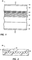
- FIG. 1 there is shown a cross section of a quantum well structure used for the Fabry-Perot light valve 30 of this invention.
- the quantum well structure is fabricated on a substrate 32 of n-doped GaAs, where the n-doping level is about 1 ⁇ 1018/cm3.
- a layer 34 of n-doped GaAs with a thickness of 0.1 ⁇ m is grown as a buffer layer.
- a multiple layer reflector 36 is grown over the buffer layer 34.
- Reflector layer 36 comprises 25 periods of 522 A° layers of In 0.5 Al 0.5 P alternating with 484 A° layers of In 0.5 (Al 0.2 Ga 0.8 ) 0.5 P.
- the multiple quantum well layer 38 which is 0.36 to 0.45 ⁇ m thick consists of 20 to 25 periods of undoped 120 A° layers of Ga 0.5 In 0.5 P alternating with undoped 60 A° layers of In 0.5 (Al 0.5 Ga 0.5 ) 0.5 P.
- a spacer/contact layer 40 of p-doped In 0.5 (Al 0.2 Ga 0.8 ) 0.5 P with a thickness of about 0.5 ⁇ m and doping of 5 ⁇ 1017 /cm3 or greater.
- a top contact 42 of the structure is a 200 A° thin film of Au.
- the quantum well structure 30 shown in Figure 1 when connected to a suitable voltage is capable of reflecting or absorbing a light beam depending on the applied voltage.
- a portion of the incident light beam is reflected from layer 42 while a second portion of the incident beam is coupled into the Fabry-Perot structure formed by layer 42 and reflector 36.
- the latter portion undergoes multiple passes through layer 40 and multiple quantum well layer 38 as it is repeatedly reflected by reflector 36 and layer 42.
- the amplitudes of these multiple reflections add coherently to the amplitude of the incident light directly reflected by layer 42.
- the optical length from layer 42 to reflector 36 and back is chosen such that the multiple reflected amplitudes are out of phase with the direct reflection from layer 42 and thus interfere destructively.
- the Fabry-Perot cavity formed between the top contact layer 42 and reflector 36 is asymmetric, i.e. the amplitude reflected by layer 36 is greater than the amplitude reflected by layer 42.
- the amplitude of the light reflected by layer 36 is greater than the amplitude of the light reflected by layer 42, thereby producing a net reflection from light valve 30.
- application of a voltage to light valve 30 produces optical absorption of the light in layer 38, thereby reducing the amplitude of the light at layer 42 from reflection off layer 36. For the level of voltage which produces enough absorption to make the amplitude of light reflected from reflector 36 equal to the amplitude of the light reflected from layer 42, complete cancellation occurs and the net reflection from light valve 30 is zero.
- a voltage in the range of 3 to 10 volts causes the light valve to absorb the incident light beam and a voltage in the neighborhood of 0 volts causes the light valve 30 to stay in the neutral state where it reflects the incident light beam.
- the structure of the quantum well can be designed to reflect the light beam when a voltage in the range of 3- to 10 volts is applied and to absorb the light beam when a voltage in the neighborhood of 0 volts is applied.
- each cylinder can be defined by proton bombardment, impurity induced layer disordering, or etch and regrowth techniques, which are well known to those skilled in the art. Therefore, each substrate can contain a plurality of cylindrical light valves.
- the individual light valves can be designed to be in an array format meaning that they can be designed to be aligned on one straight line. Also, the number of light valves can be designed to be equal to the number of pixels on one scan line.
- each cylindrical light valve which also was referred to as an element of a light valve array, will be called a "cell".
- a top view of a modulator 50 with a plurality of cells C there is shown a top view of a modulator 50 with a plurality of cells C.
- the modulator comprises a single array of cells C each of which corresponds to one pixel on a photoreceptor. Each one of these cells is independent of the other cells and each one is addressed individually.
- the cross section of each cell is illustrated as a circle in Figure 2 but could equally well be elliptical, rectangular, or any other shaped desired of each pixel.
- the top layer 46 surrounding the cells C should be made of a reflective material, but for write-black imaging systems, the top layer 46 surrounding the cells C should be made of a non reflective material.
- a laser diode light source 62 emits a coherent light beam 64 which is collimated in the sagittal and tangential directions by a spherical lens system 66.
- the collimated light beam from lens 66 is passed through a polarizing beamsplitter 68 and a ⁇ /4 retardation plate 72.
- the polarizing beamsplitter 68 polarizes the incident beam or passes the incident beam if the laser emitted a polarized light beam.
- Retardation plate 72 rotates the plane of linear polarization by 45 degrees.
- Cylindrical lens 74 focuses the collimated beam to a virtual point 76 which is refocused and then collimated by the cylindrical front surface of toric lens 78 onto light valve array 80. In the sagittal direction, the collimated beam is not changed by cylindrical lens 74 but is focussed by the cylindrical back surface of toric lens 78 to a wedge-shaped beam forming a focussed line image on light valve array 80.
- Light beam 82 is reflected by non-activated cells of light valve array 80 and absorbed by activated cells of light valve array 80 to form a pixelatted line image.
- Light reflected from the array is imaged back through lenses 78 and 74 to retardation plate 72.
- Retardation plate 72 rotates the plane of polarization by another 45 degrees, thereby making its polarization orthogonal to the polarization transmitted by the polarizing beamsplitter. Consequently polarizing beamsplitter 68 reflects the backward traveling beam to lens system 84 which images the pixelatted line image onto photoreceptor 88 to form a latent image.
- the light beam 64 from the laser light source 62 has a Gaussian-like intensity distribution. However, in order to illuminate all the cells C of the light valve array 80 with a uniform intensity, the intensity of the light beam 64 has to be modified to have a uniform distribution over the entire width of the array.
- the two lenses 74 and 78 modify the Gaussian distribution of the light beam 64 to a uniform intensity distribution. It should be noted that any optical system which can modify the intensity of the light beam 64 to a uniform intensity can be utilized to replace the two lenses 74 and 78.
- lens 74 is a cylindrical lens with power in the tangential plane
- lens 78 is a toric lens comprised of a front surface having power only in the tangential plane and a back surface having power only in the sagittal plane.
- FIG 4 there is shown a magnified view of the light valve array used in the printing system 60 of this invention.
- the light valve array 80 utilized in this invention has 5100 cells, for 24 spots per mm (600 spi), each of which corresponds to a pixel on a 216mm (8.5 inch) scan line.
- the light valve array will be about 3 cm long to cover a 216mm (8.5 inch) scan line. Therefore, the overall magnification of the optical system is 7.2.
- the light valve array should have a center-to-center spacing equal to 5.9 ⁇ m.
- the number of pixels in the light valve array can be designed to match the pixel density required of that printing system. For example, if the printing system has 12 pixels/mm (300 pixels/inch), the light valve array will have 2550 cells in the tangential direction. Each cell of the light valve array 80 is individually addressable and depending on the train of pixel information, the cells are selectively addressed and activated to absorb the light.
- FIG. 5 there is shown a train of pixel information that is used to activate the cells in Figure 4.
- pixel P1, P3, P4, P6, P7 and P5099 are 1 and therefore cells C1, C3, C4, C6, C7 and P5099 are activated to absorb the light beam.
- the photoreceptor 88 receives no light spots at pixel P1, P3, P4, P6, P7, and P5099.
- the train of pixel information contains a 0 for pixels P2, P5 and P5100, the cells C2, C5 and C5100 do not receive voltage and therefore reflect the light.
- the photoreceptor 88 receives light spots for the pixels P2, P5 and P5100.
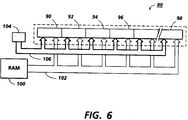
- FIG. 6 shows a method of applying the pixel information to the light valve array 80 to activate the cells that are needed to absorb the light beam.
- Each one of the boxes 90, 92, 94, 96 and 98 represents a group of 16 cells of the light valve array 80.
- the train of pixel information is stored in a random access memory (RAM) 100 which will be transferred to the cells via a 16-bit bus 102.
- RAM random access memory
- a controlling processor 104 selects one group of the cells 90, 92, 94, 96 and 98 through an address bus 106.
- the number of the bits on the address bus varies with the number of the cells used in each system.
- 16-bits of data will be delivered to one group of 16 cells. Each cell will receive one bit of data and if the data is a 1, the cell will be activated to absorb and if the data is a 0 the cell will be left in its neutral state which then reflects the light beam. On the next clock cycle, the following 16-bits of data will be delivered to the second group of 16 cells. After each cell receives a bit of data, the cell will retain that data until it receives a reset or new data. When the last cells in the array have received their data, the controlling processor will send out a flag indicating that the array is ready to transfer the information for that scan line.
- the laser diode will be activated to illuminate the light valve array 80.
- the light beam illuminates the array only as long as needed to print the line, thereby avoiding pixel smear in the sagittal direction as well as reducing heat generated in the laser and the light valve array and extending the life of the laser source.
- the light valve array reflects light onto the photoreceptor plane from those cells that are not activated.
- the pixel information transfer rate for one scan line with the fastest commercial conventional printing systems is about 113 microsecond. However, the pixel information transfer rate for one scan line of this invention is 25 microsecond. This system is capable of transferring the data onto the photoreceptor at a printing speed of 1000 pages per minute which is an enormous improvement over the existing printing systems.
- the same concept can be applied to design a modulator with multiple arrays of cells to provide simultaneous reflection of all pixel information in one text line.
- the modulator 86 has enough rows, e.g. 5 to cover all the sagittal pixels of the letter A.
- the number of scan lines which are needed to produce a text line is much more than 5.
- cells Cb are all activated to simultaneously absorb all the necessary pixels and cells Ca are left in their neutral state to simultaneously reflect all the necessary pixels to print the letter A.
- this concept can be expanded to design of a 2-dimensional light valve array which has enough rows and columns of cells to simultaneously reflect the pixel information of an entire page or image onto the photoreceptor.
- the printing system of this invention is more efficient in the use of light since the light source is turned on only when the pixel information is delivered to the light valve array and the light valves are ready to reflect or absorb the light.
- the light valve array used in this invention can also be used to control the amount of light being reflected by the light valves.
- the shape of the pixels on the photoreceptor plane can be controlled by the shape of the valves which can be designed to have a desired shape such as a circle or a square.
- utilizing a Fabry-Perot light valve array provides the possibility of fabricating a small, high density chip using well-known techniques of semiconductor manufacture. The use of wafer-scale manufacturing decreases the fabrication cost and simplifies the fabrication of a page wide light valve array. In addition, due to the efficiency in the use of light, the power requirement on the light source will be lowered.
- the printing system of this invention can be used to write white or write black.
Landscapes
- Printers Or Recording Devices Using Electromagnetic And Radiation Means (AREA)
Applications Claiming Priority (2)
| Application Number | Priority Date | Filing Date | Title |
|---|---|---|---|
| US08/158,559 US5414553A (en) | 1993-11-29 | 1993-11-29 | Electroabsorptive asymmetrical fabry-perot modulator array for line printers |
| US158559 | 1993-11-29 |
Publications (3)
| Publication Number | Publication Date |
|---|---|
| EP0655341A2 true EP0655341A2 (fr) | 1995-05-31 |
| EP0655341A3 EP0655341A3 (fr) | 1998-01-07 |
| EP0655341B1 EP0655341B1 (fr) | 2001-10-24 |
Family
ID=22568689
Family Applications (1)
| Application Number | Title | Priority Date | Filing Date |
|---|---|---|---|
| EP94308747A Expired - Lifetime EP0655341B1 (fr) | 1993-11-29 | 1994-11-28 | Dispositif de modulateur électroabsorbant asymétrique du type fabry-pérot pour imprimantes par lignes |
Country Status (5)
| Country | Link |
|---|---|
| US (1) | US5414553A (fr) |
| EP (1) | EP0655341B1 (fr) |
| JP (1) | JPH07199132A (fr) |
| CA (1) | CA2117703C (fr) |
| DE (1) | DE69428760T2 (fr) |
Cited By (2)
| Publication number | Priority date | Publication date | Assignee | Title |
|---|---|---|---|---|
| DE102010002278A1 (de) | 2009-02-26 | 2010-09-02 | C. Rob. Hammerstein Gmbh & Co. Kg | Höhenverstellbarer Kraftfahrzeugsitz mit einem Spindelantrieb |
| CN110133771A (zh) * | 2019-05-31 | 2019-08-16 | 江南大学 | 一种利用结构对称性破缺实现超窄带吸收和传感的方法 |
Families Citing this family (3)
| Publication number | Priority date | Publication date | Assignee | Title |
|---|---|---|---|---|
| US5754217A (en) * | 1995-04-19 | 1998-05-19 | Texas Instruments Incorporated | Printing system and method using a staggered array spatial light modulator having masked mirror elements |
| CA2170198C (fr) * | 1996-02-23 | 2000-07-25 | Stephen Keating | Systeme de panneaux muraux mobiles et methode d'utilisation correspondante |
| US6330018B1 (en) * | 1999-12-22 | 2001-12-11 | Eastman Kodak Company | Method and apparatus for printing high resolution images using reflective LCD modulators |
Family Cites Families (9)
| Publication number | Priority date | Publication date | Assignee | Title |
|---|---|---|---|---|
| US4376568A (en) * | 1981-01-12 | 1983-03-15 | Xerox Corporation | Thick film line modulator |
| US4413270A (en) * | 1981-03-30 | 1983-11-01 | Xerox Corporation | Multigate light valve for electro-optic line printers having non-telecentric imaging systems |
| US4377753A (en) * | 1981-06-01 | 1983-03-22 | Eastman Kodak Company | High resolution optical-addressing device and electronic scanner and/or printer apparatus employing such device |
| US4848879A (en) * | 1982-10-09 | 1989-07-18 | Canon Kabushiki Kaisha | Light modulating device |
| LU86777A1 (fr) * | 1987-02-13 | 1988-03-02 | Europ Communities | Lichtmodulator auf der basis eines nicht-linearen fabry-perot-mehrschichteninterferenzfilters |
| US4801194A (en) * | 1987-09-23 | 1989-01-31 | Eastman Kodak Company | Multiplexed array exposing system having equi-angular scan exposure regions |
| US5081597A (en) * | 1989-12-21 | 1992-01-14 | Xerox Corporation | Process for dynamically equalizing multichannel optical imaging systems |
| US5157538A (en) * | 1990-06-29 | 1992-10-20 | The United States Of America As Represented By The Secretary Of The Air Force | Silicon spatial light modulator |
| JP2856952B2 (ja) * | 1991-08-13 | 1999-02-10 | シャープ株式会社 | 光演算装置 |
-
1993
- 1993-11-29 US US08/158,559 patent/US5414553A/en not_active Expired - Lifetime
-
1994
- 1994-09-19 CA CA002117703A patent/CA2117703C/fr not_active Expired - Fee Related
- 1994-11-21 JP JP28634194A patent/JPH07199132A/ja active Pending
- 1994-11-28 EP EP94308747A patent/EP0655341B1/fr not_active Expired - Lifetime
- 1994-11-28 DE DE69428760T patent/DE69428760T2/de not_active Expired - Lifetime
Cited By (2)
| Publication number | Priority date | Publication date | Assignee | Title |
|---|---|---|---|---|
| DE102010002278A1 (de) | 2009-02-26 | 2010-09-02 | C. Rob. Hammerstein Gmbh & Co. Kg | Höhenverstellbarer Kraftfahrzeugsitz mit einem Spindelantrieb |
| CN110133771A (zh) * | 2019-05-31 | 2019-08-16 | 江南大学 | 一种利用结构对称性破缺实现超窄带吸收和传感的方法 |
Also Published As
| Publication number | Publication date |
|---|---|
| DE69428760D1 (de) | 2001-11-29 |
| CA2117703C (fr) | 1999-07-13 |
| CA2117703A1 (fr) | 1995-05-30 |
| DE69428760T2 (de) | 2002-05-08 |
| JPH07199132A (ja) | 1995-08-04 |
| US5414553A (en) | 1995-05-09 |
| EP0655341A3 (fr) | 1998-01-07 |
| EP0655341B1 (fr) | 2001-10-24 |
Similar Documents
| Publication | Publication Date | Title |
|---|---|---|
| US4571603A (en) | Deformable mirror electrostatic printer | |
| US5208456A (en) | Apparatus and system for spot position control in an optical output device employing a variable wavelength light source | |
| EP0077188B1 (fr) | Modulateur électrooptique | |
| JPH11337891A (ja) | 格子変調器アレイ | |
| US4560994A (en) | Two dimensional electro-optic modulator for printing | |
| US4973121A (en) | Scanner | |
| EP0123425B1 (fr) | Imprimante électro-optique à canaux multiples | |
| US4730331A (en) | Superluminescent LED source | |
| CA1176742A (fr) | Modulateur de ligne a couche epaisse | |
| US4638334A (en) | Electro-optic line printer with super luminescent LED source | |
| EP1433011B1 (fr) | Systeme optique actif permettant de dephaser des parties determinees d'un front d'onde optique entrant | |
| WO1989012369A1 (fr) | Systeme de scanner a laser multi-faisceau | |
| US5414553A (en) | Electroabsorptive asymmetrical fabry-perot modulator array for line printers | |
| US5204523A (en) | Method for spot position control in an optical output device employing a variable wavelength light source and an optical beam deflecting element | |
| US5264869A (en) | Electro-optical control apparatus and system for spot position control in an optical output device | |
| JPS637369B2 (fr) | ||
| EP0437596B1 (fr) | Dispositif de balayage | |
| GB2123247A (en) | Facsimile reproduction scanner | |
| US4557563A (en) | Two dimensional electro-optic modulator for optical processing | |
| US5212381A (en) | Method of controlling slow scan direction of spot position in an optical output device employing an electro-optical control apparatus | |
| US20010050707A1 (en) | Image recording apparatus | |
| EP0532133A2 (fr) | Réseau à laser | |
| WO1991017473A2 (fr) | Modulateur multicanal a optique integree pour imprimante laser | |
| JP2000507004A (ja) | 増大した角度走査範囲を有する光学装置 | |
| EP0528543B1 (fr) | Procédé et appareil pour contrÔler la position d'un spot lumineux |
Legal Events
| Date | Code | Title | Description |
|---|---|---|---|
| PUAI | Public reference made under article 153(3) epc to a published international application that has entered the european phase |
Free format text: ORIGINAL CODE: 0009012 |
|
| AK | Designated contracting states |
Kind code of ref document: A2 Designated state(s): DE FR GB IT |
|
| PUAL | Search report despatched |
Free format text: ORIGINAL CODE: 0009013 |
|
| AK | Designated contracting states |
Kind code of ref document: A3 Designated state(s): DE FR GB IT |
|
| 17P | Request for examination filed |
Effective date: 19980707 |
|
| 17Q | First examination report despatched |
Effective date: 19990625 |
|
| GRAG | Despatch of communication of intention to grant |
Free format text: ORIGINAL CODE: EPIDOS AGRA |
|
| GRAG | Despatch of communication of intention to grant |
Free format text: ORIGINAL CODE: EPIDOS AGRA |
|
| GRAH | Despatch of communication of intention to grant a patent |
Free format text: ORIGINAL CODE: EPIDOS IGRA |
|
| GRAH | Despatch of communication of intention to grant a patent |
Free format text: ORIGINAL CODE: EPIDOS IGRA |
|
| GRAA | (expected) grant |
Free format text: ORIGINAL CODE: 0009210 |
|
| AK | Designated contracting states |
Kind code of ref document: B1 Designated state(s): DE FR GB IT |
|
| REF | Corresponds to: |
Ref document number: 69428760 Country of ref document: DE Date of ref document: 20011129 |
|
| REG | Reference to a national code |
Ref country code: GB Ref legal event code: IF02 |
|
| ET | Fr: translation filed | ||
| PLBE | No opposition filed within time limit |
Free format text: ORIGINAL CODE: 0009261 |
|
| STAA | Information on the status of an ep patent application or granted ep patent |
Free format text: STATUS: NO OPPOSITION FILED WITHIN TIME LIMIT |
|
| 26N | No opposition filed | ||
| PGFP | Annual fee paid to national office [announced via postgrant information from national office to epo] |
Ref country code: DE Payment date: 20101124 Year of fee payment: 17 |
|
| PGFP | Annual fee paid to national office [announced via postgrant information from national office to epo] |
Ref country code: IT Payment date: 20101117 Year of fee payment: 17 Ref country code: GB Payment date: 20101124 Year of fee payment: 17 |
|
| PGFP | Annual fee paid to national office [announced via postgrant information from national office to epo] |
Ref country code: FR Payment date: 20111118 Year of fee payment: 18 |
|
| GBPC | Gb: european patent ceased through non-payment of renewal fee |
Effective date: 20121128 |
|
| REG | Reference to a national code |
Ref country code: FR Ref legal event code: ST Effective date: 20130731 |
|
| PG25 | Lapsed in a contracting state [announced via postgrant information from national office to epo] |
Ref country code: IT Free format text: LAPSE BECAUSE OF NON-PAYMENT OF DUE FEES Effective date: 20121128 |
|
| REG | Reference to a national code |
Ref country code: DE Ref legal event code: R119 Ref document number: 69428760 Country of ref document: DE Effective date: 20130601 |
|
| PG25 | Lapsed in a contracting state [announced via postgrant information from national office to epo] |
Ref country code: DE Free format text: LAPSE BECAUSE OF NON-PAYMENT OF DUE FEES Effective date: 20130601 |
|
| PG25 | Lapsed in a contracting state [announced via postgrant information from national office to epo] |
Ref country code: FR Free format text: LAPSE BECAUSE OF NON-PAYMENT OF DUE FEES Effective date: 20121130 Ref country code: GB Free format text: LAPSE BECAUSE OF NON-PAYMENT OF DUE FEES Effective date: 20121128 |