EP0655614A1 - Circuit intégré à circuit thermique sur puce ne nécessitant qu'une borne dédicacée et méthode de fonctionnement - Google Patents
Circuit intégré à circuit thermique sur puce ne nécessitant qu'une borne dédicacée et méthode de fonctionnement Download PDFInfo
- Publication number
- EP0655614A1 EP0655614A1 EP94118577A EP94118577A EP0655614A1 EP 0655614 A1 EP0655614 A1 EP 0655614A1 EP 94118577 A EP94118577 A EP 94118577A EP 94118577 A EP94118577 A EP 94118577A EP 0655614 A1 EP0655614 A1 EP 0655614A1
- Authority
- EP
- European Patent Office
- Prior art keywords
- integrated circuit
- pin
- die
- circuit
- temperature
- Prior art date
- Legal status (The legal status is an assumption and is not a legal conclusion. Google has not performed a legal analysis and makes no representation as to the accuracy of the status listed.)
- Withdrawn
Links
Images
Classifications
-
- H—ELECTRICITY
- H10—SEMICONDUCTOR DEVICES; ELECTRIC SOLID-STATE DEVICES NOT OTHERWISE PROVIDED FOR
- H10D—INORGANIC ELECTRIC SEMICONDUCTOR DEVICES
- H10D89/00—Aspects of integrated devices not covered by groups H10D84/00 - H10D88/00
- H10D89/60—Integrated devices comprising arrangements for electrical or thermal protection, e.g. protection circuits against electrostatic discharge [ESD]
-
- G—PHYSICS
- G01—MEASURING; TESTING
- G01K—MEASURING TEMPERATURE; MEASURING QUANTITY OF HEAT; THERMALLY-SENSITIVE ELEMENTS NOT OTHERWISE PROVIDED FOR
- G01K7/00—Measuring temperature based on the use of electric or magnetic elements directly sensitive to heat ; Power supply therefor, e.g. using thermoelectric elements
- G01K7/01—Measuring temperature based on the use of electric or magnetic elements directly sensitive to heat ; Power supply therefor, e.g. using thermoelectric elements using semiconducting elements having PN junctions
-
- H—ELECTRICITY
- H10—SEMICONDUCTOR DEVICES; ELECTRIC SOLID-STATE DEVICES NOT OTHERWISE PROVIDED FOR
- H10W—GENERIC PACKAGES, INTERCONNECTIONS, CONNECTORS OR OTHER CONSTRUCTIONAL DETAILS OF DEVICES COVERED BY CLASS H10
- H10W40/00—Arrangements for thermal protection or thermal control
Definitions
- the present invention generally relates to integrated circuits, and more particularly, to the monitoring of thermal characteristics of an operating integrated circuit.
- An important operating characteristic of an integrated circuit is the temperature of the integrated circuit's die when the integrated circuit is fully powered and in a normal operating mode of operation. Such a temperature measurement is often desired at a final package test when the integrated circuit is in the same form as will be used by an end user. To satisfy this need, others have used an on-chip resistor connected to two dedicated external pins of the integrated circuit. The external pins have no other function than to implement the temperature measurement function.
- An example of an integrated circuit having two dedicated pins for temperature measurement of the integrated circuit die is the MC88110 reduced instruction set microprocessor.
- the temperature of the integrated circuit having an on-chip resistor is measured by using a current source reference and forcing a known current thru the known resistance of the on-chip resistor. A resulting voltage across the two dedicated integrated circuit pins is then measured. The resulting voltage is proportional to the temperature of the operating integrated circuit. In other words, as the temperature of the operating integrated circuit die varies, the resistance varies proportionately which results in a proportional change in voltage measured across the two dedicated integrated circuit pins.
- the two dedicated integrated circuit pins are required in order to isolate internally generated noise and other circuit parameters from the two integrated circuit pins. Any voltage, current, resistance or impedance which is coupled to the two integrated circuit pins from internal to the integrated circuit will modify the voltage potential between the two integrated circuit pins and result in an incorrect temperature measurement.
- the price of two dedicated integrated circuit pins to implement a measurement function is costly, even in the most advanced very large scale integrated circuits.
- resistor network integrated circuit Another type of integrated circuit which uses a plurality of resistors connected between the integrated circuit's external pins is a resistor network integrated circuit.
- this type of integrated circuit functions only to provide a user with a plurality of possible resistance values depending upon which pins of the integrated circuit are connected. No other operating circuitry is typically implemented in such circuits.
- Yet another known type of integrated circuit which provides a signal from which an operating die temperature may be derived utilizes a significant amount of dedicated internal circuitry, such as an analog-to-digital (A/D) circuit and a storage register, to provide the signal at a single dedicated output pin of the integrated circuit.
- A/D analog-to-digital
- storage register to provide the signal at a single dedicated output pin of the integrated circuit.
- the additional internal circuitry which is required to implement this temperature measurement function is often prohibitive in many large scale integration designs.
- an integrated circuit having an on chip thermal circuit requiring only one dedicated integrated circuit pin and a method of implementing a single pin on chip thermal circuit in an integrated circuit.
- the integrated circuit comprises a die and a first integrated circuit pin which is dedicated solely for use with the on chip thermal circuit.
- a second integrated circuit pin is also provided.
- An integrated circuit die thermal sensing circuit is located on the die and directly connected to the first integrated circuit pin and to the second integrated circuit pin.
- the integrated circuit die thermal sensing circuit comprises a material which has a physical characteristic which varies in a manner proportional to variation of temperature of the material.
- a functional operating circuit is located on the die and is connected directly to the second integrated circuit pin.
- the functional operating circuit performs a predetermined operating function within the integrated circuit at the same time the integrated circuit die thermal sensing circuit provides an output signal which indicates an operating temperature of the die.
- the second integrated circuit pin is used by both the integrated circuit die thermal sensing circuit and the functional operating circuit.
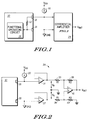
- FIG. 1 Illustrated in FIG. 1 is an integrated circuit die 10 in accordance with the present invention. Although not fully illustrated as a packaged integrated circuit for purposes of illustrating the present invention, integrated circuit die 10 should be considered as a fully encapsulated die in a completed integrated circuit chip.
- Integrated circuit die 10 generally has a die thermal sensing circuit 12, a functional operating circuit 14, a first integrated circuit pin 16, and a second integrated circuit pin 18. Also illustrated is a constant current source 20 and a differential amplifier 24.
- die thermal sensing circuit 12 is implemented as a resistor having a first terminal connected to first integrated circuit pin 16 and having a second terminal connected to second integrated circuit pin 18.
- the second integrated circuit pin 18 is a ground reference pin of integrated circuit die 10.
- Functional operating circuit 14 has a terminal connected directly to the second integrated circuit pin 18, thereby making the second integrated circuit pin a common integrated circuit pin which is common to both the die thermal sensing circuit 12 and the functional operating circuit 14.
- a constant current source 20 has a first terminal connected to a power supply voltage, such as V DD , and has a second terminal connected to both the first integrated circuit pin 16 and a first input of differential amplifier 24.
- a second input of differential amplifier 24 is connected to the second integrated circuit pin 18.
- An output of differential amplifier 24 provides an output voltage, Vout, which is referenced to a ground reference terminal and is proportional to temperature.
- an operating temperature of integrated circuit die 10 may be accurately measured while circuit die 10 is fully operational. Further, this function only requires one dedicated integrated circuit pin, the first integrated circuit pin because the second integrated circuit pin is used concurrently by the functional operating circuit 14.
- Functional operating circuit 14 performs a predetermined operating function within the integrated circuit 10 at the same time the present invention is utilized to determine the die operating temperature. Examples of the functionality of operating circuit 14 might include an execution unit, digital logic circuitry, address translation circuitry, a memory, etc..
- the die thermal sensing circuit 12 is implemented as a resistor. If a metal resistor is utilized, a resistor may be formed which is susceptible to average temperature changes of the integrated circuit die 10 and which provides a temperature coefficient of approximately 1.2 Ohms/degree Centigrade.
- die thermal sensing circuit 12 As constant current source 20 provides a constant reference current to integrated circuit die 10, a small predetermined voltage is developed across the resistance of die thermal sensing circuit 12.
- the temperature coefficient depends upon what material is selected as die thermal sensing circuit 12, but is conventionally known for a given temperature range.
- die thermal sensing circuit 12 As the die temperature changes, so does the resistance of die thermal sensing circuit 12. An increase in die temperature causes an increase in the resistance of die thermal sensing circuit 12, and a decrease in die temperature causes a decrease in the resistance of die thermal sensing circuit 12. Since the current through the resistance of die thermal sensing circuit 12 is constant, the voltage which is developed across the resistance of die thermal sensing circuit 12 is also proportional to the temperature of the die. In other words, when the die temperature increases the voltage between the first integrated circuit pin 16 and the second integrated circuit pin 18 increases, and vice versa.
- the amount of electrical current normally channeled to or "sunk" by a ground terminal from the functional operating circuit 14 can be substantial causing the ground potential to actually rise above zero volts.
- Such an operating condition would therefore create an error voltage between the first integrated circuit pin 16 and the second integrated circuit pin 18.
- the error voltage is known in the art by the term "ground bounce".
- the present invention however can still be utilized even when ground bounce errors exist.
- the voltage variation across the resistance of die thermal sensing circuit 12 attributable to ground bounce is common mode with respect to the ground bounce voltage variation at the common or second integrated circuit pin 18.
- Differential amplifier 24 may be used to subtract the common mode ground bounce noise from the output voltage between integrated circuit pins 16 and 18. Differential amplifier 24 therefore recovers a pure voltage which is proportional to the resistance of die thermal sensing circuit 12. In other words, differential amplifier 24 removes a common mode error component from a voltage differential between the first and second integrated circuit pins. Although two integrated circuit pins are utilized, it should be noted that the common or second integrated circuit pin 18 is already present on the integrated circuit and is never taken out of operational use during the die thermal measuring process.
- FIG. 2 Illustrated in FIG. 2 is a detailed diagram of one form of a differential amplifier which may be used as differential amplifier 24 in connection with constant current source 20 and integrated circuit die 10. Elements in FIG. 2 which are the same as elements in FIG. 1 are identically numbered for clarification.
- Differential amplifier 24 has a first operational amplifier 31 having a first, noninverting (positive) input connected to integrated circuit pin 16.
- constant current source 20 has the first terminal thereof connected to power supply voltage V D D and the second terminal thereof connected to integrated circuit pin 16 of integrated circuit die 10.
- a second, inverting (negative) input of operational amplifier 31 is connected to an output thereof and to a first terminal of a resistor 33.
- a second terminal of resistor 33 is connected to a first terminal of a resistor 35.
- a second operational amplifier 37 has a first, noninverting (positive) input connected to integrated circuit pin 18 which is a ground terminal on the integrated circuit package and therefore connected to ground.
- a second, inverting (negative) input of operational amplifier 31 is connected to an output thereof and to a first terminal of a resistor 39.
- a second terminal of resistor 39 is connected to a first, noninverting (positive) input of a third operational amplifier 41 and to a first terminal of a resistor 43.
- a second terminal of resistor 43 is connected to a ground reference terminal.
- a second, inverting (negative) input of operational amplifier 41 is connected to both the second terminal of resistor 33 and the first terminal of resistor 35.
- a second terminal of resistor 35 is connected to an output of operational amplifier 41 and provides the output voltage Vout.
- the three operational amplifiers may be obtained by using the commercially available integrated circuit LF347 from National Semiconductor Corporation which contains four operational amplifiers.
- a fourth operational amplifier of an LF347 integrated circuit may be used as
- operational amplifiers 31 and 37 are high impedance unity gain buffer stages which do not load integrated circuit pins 16 and 18.
- Operational amplifier 41 is configured as a differential amplifier and resistors 33, 35, 39 and 43 function to establish a gain of differential amplifier 24.
- resistors 33 and 39 have the same resistance, R1, and assume that resistors 35 and 43 have the same resistance R2.
- the output voltage of operational amplifier 31 is V R referenced to a ground potential
- the output voltage of operational amplifier 37 is V G referenced to the ground potential.
- Vout [(R2)/(R1)] * [V G - V R ] (2) where R1 is the resistance of each of resistors 33 and 39, and R2 is the resistance of each of resistors 35 and 43.
- the ground bounce noise is totally subtracted from the output voltage as a result of the subtraction of V R from V G .
- each of the V R and V G voltages is referenced to ground, and noise bounce which is injected into the ground is therefore neutralized and invisible to the final output voltage provided by differential amplifier 24.
- ground reference terminal pin any ground reference terminal may be used to implement the present invention but it is preferable to connect differential amplifier 24 to the same ground pin which the die thermal sensing circuit 18 is connected to. If other ground pins are connected to differential amplifier 24 than the ground pin which die thermal sensing circuit 18 is connected to, inductance and other electrical properties may create differential voltage potentials between the various ground circuit pins when the integrated circuit is operational.
- the present invention may alternately be used without the assistance of external differential amplifier 24 and constant current source 20.
- the resistance of die thermal sensing circuit 12 of integrated circuit die 10 may be measured at room temperature between integrated circuit pins 16 and 18 before the integrated circuit is powered up. Then the integrated circuit may be powered up and is operational for a sufficient amount of time to allow the die to achieve a characteristic operating die temperature. The power should then be disconnected from the integrated circuit and another resistance measurement of the die thermal sensing circuit 12 immediately made.
- the differing resistance values can be used in accordance with equation 1 to provide an average operating temperature of the integrated circuit. In this technique, ground bounce noise does not exist and is therefore irrelevant.
- an integrated circuit having an on chip thermal circuit requiring only one dedicated integrated circuit pin, and a method of operating the unique integrated circuit.
- An advantage of the present invention is the saving of an additional dedicated integrated circuit pin to provide a die temperature when the die is powered up and operational.
- any fixed voltage potential integrated circuit pin may be used to implement the function of the common integrated circuit pin 18.
- any type of circuitry whether digital or analog and regardless of process type, may be used as the functional circuitry which is connected to the common integrated circuit pin 18.
- the present invention may be implemented by establishing a fixed voltage across the die thermal sensing circuit 12 and measuring the current thru die thermal sensing circuit 12 which is proportional to die temperature.
Landscapes
- Physics & Mathematics (AREA)
- General Physics & Mathematics (AREA)
- Semiconductor Integrated Circuits (AREA)
Applications Claiming Priority (2)
| Application Number | Priority Date | Filing Date | Title |
|---|---|---|---|
| US158323 | 1993-11-29 | ||
| US08/158,323 US5376819A (en) | 1993-11-29 | 1993-11-29 | Integrated circuit having an on chip thermal circuit requiring only one dedicated integrated circuit pin and method of operation |
Publications (1)
| Publication Number | Publication Date |
|---|---|
| EP0655614A1 true EP0655614A1 (fr) | 1995-05-31 |
Family
ID=22567595
Family Applications (1)
| Application Number | Title | Priority Date | Filing Date |
|---|---|---|---|
| EP94118577A Withdrawn EP0655614A1 (fr) | 1993-11-29 | 1994-11-25 | Circuit intégré à circuit thermique sur puce ne nécessitant qu'une borne dédicacée et méthode de fonctionnement |
Country Status (3)
| Country | Link |
|---|---|
| US (2) | US5376819A (fr) |
| EP (1) | EP0655614A1 (fr) |
| JP (1) | JP2885104B2 (fr) |
Families Citing this family (11)
| Publication number | Priority date | Publication date | Assignee | Title |
|---|---|---|---|---|
| US5376819A (en) * | 1993-11-29 | 1994-12-27 | Motorola, Inc. | Integrated circuit having an on chip thermal circuit requiring only one dedicated integrated circuit pin and method of operation |
| US5440520A (en) * | 1994-09-16 | 1995-08-08 | Intel Corporation | Integrated circuit device that selects its own supply voltage by controlling a power supply |
| US6246100B1 (en) * | 1999-02-03 | 2001-06-12 | National Semiconductor Corp. | Thermal coupler utilizing peltier and seebeck effects |
| EP1182449A1 (fr) | 2000-08-21 | 2002-02-27 | Motorola, Inc. | Appareil et méthode pour gérer un circuit intégré |
| WO2002054489A2 (fr) * | 2000-12-29 | 2002-07-11 | Advanced Micro Devices, Inc. | Systeme et procede de mesure de la temperature |
| DE10133736A1 (de) * | 2001-07-11 | 2003-01-23 | Philips Corp Intellectual Pty | Anordnung zum Messen der Temperatur einer elektronischen Schaltung |
| FR2834343B1 (fr) * | 2001-12-28 | 2004-04-09 | St Microelectronics Sa | Detecteur thermique |
| US6984064B1 (en) * | 2002-07-31 | 2006-01-10 | Advanced Micro Devices, Inc. | Thermal transfer measurement of an integrated circuit |
| US8044697B2 (en) | 2006-06-29 | 2011-10-25 | Intel Corporation | Per die temperature programming for thermally efficient integrated circuit (IC) operation |
| JP6958499B2 (ja) * | 2018-07-09 | 2021-11-02 | 三菱電機株式会社 | 半導体装置および電力変換装置 |
| US11569808B2 (en) * | 2020-11-02 | 2023-01-31 | Texas Instruments Incorporated | Wide high voltage swing input comparator stage with matching overdrive |
Citations (2)
| Publication number | Priority date | Publication date | Assignee | Title |
|---|---|---|---|---|
| US5213416A (en) * | 1991-12-13 | 1993-05-25 | Unisys Corporation | On chip noise tolerant temperature sensing circuit |
| US5230564A (en) * | 1992-03-20 | 1993-07-27 | Cray Research, Inc. | Temperature monitoring system for air-cooled electric components |
Family Cites Families (3)
| Publication number | Priority date | Publication date | Assignee | Title |
|---|---|---|---|---|
| US5140394A (en) * | 1988-07-26 | 1992-08-18 | Texas Instruments Incorporated | Electrothermal sensor apparatus |
| US5141334A (en) * | 1991-09-24 | 1992-08-25 | The United States Of America As Represented By The Administrator Of The National Aeronautics And Space Administration | Sub-kelvin resistance thermometer |
| US5376819A (en) * | 1993-11-29 | 1994-12-27 | Motorola, Inc. | Integrated circuit having an on chip thermal circuit requiring only one dedicated integrated circuit pin and method of operation |
-
1993
- 1993-11-29 US US08/158,323 patent/US5376819A/en not_active Expired - Lifetime
-
1994
- 1994-08-29 US US08/297,280 patent/US5477076A/en not_active Expired - Fee Related
- 1994-11-25 EP EP94118577A patent/EP0655614A1/fr not_active Withdrawn
- 1994-11-28 JP JP6316000A patent/JP2885104B2/ja not_active Expired - Fee Related
Patent Citations (2)
| Publication number | Priority date | Publication date | Assignee | Title |
|---|---|---|---|---|
| US5213416A (en) * | 1991-12-13 | 1993-05-25 | Unisys Corporation | On chip noise tolerant temperature sensing circuit |
| US5230564A (en) * | 1992-03-20 | 1993-07-27 | Cray Research, Inc. | Temperature monitoring system for air-cooled electric components |
Also Published As
| Publication number | Publication date |
|---|---|
| JP2885104B2 (ja) | 1999-04-19 |
| US5376819A (en) | 1994-12-27 |
| JPH07193185A (ja) | 1995-07-28 |
| US5477076A (en) | 1995-12-19 |
Similar Documents
| Publication | Publication Date | Title |
|---|---|---|
| AU731610B2 (en) | Capacitance detection system and method | |
| US6736540B1 (en) | Method for synchronized delta-VBE measurement for calculating die temperature | |
| JP4915658B2 (ja) | 蓄電池セルの端子電圧及び内部インピーダンス測定回路 | |
| US5376819A (en) | Integrated circuit having an on chip thermal circuit requiring only one dedicated integrated circuit pin and method of operation | |
| JPH05223887A (ja) | 電力用mos形トランジスタの電流測定回路 | |
| CN104457817A (zh) | 一种单芯片集成的传感器信号调理电路 | |
| JP3313773B2 (ja) | 半導体装置 | |
| US20240061025A1 (en) | Current sensing circuit | |
| EP0744837B1 (fr) | Circuit d'entrée pour un signal analogique comprenant un convertisseur analogique-numérique dans un circuit à semi-conducteurs | |
| US5293327A (en) | Method of logic circuit simulation | |
| CN206556780U (zh) | 温度检测装置 | |
| US20220357375A1 (en) | Current sensing circuit | |
| CN112697343A (zh) | 电阻桥式压力传感器的检测电路、方法、电子设备及芯片 | |
| JP2898500B2 (ja) | 温度特性補正付圧力センサ | |
| CN115950570B (zh) | 压力测量电路、芯片及电子设备 | |
| US7026828B2 (en) | Recording module with a universal input for measurement of physical parameters | |
| CN219244853U (zh) | 压力测量电路、压力检测电路、芯片及电子设备 | |
| CN113017588B (zh) | 一种血压测量方法、系统、装置及血压计 | |
| JP2005003596A (ja) | 抵抗測定装置、抵抗測定用集積回路及び抵抗測定方法 | |
| US6314544B1 (en) | Characterization procedure for a voltage converter connected to a capacitive circuit | |
| CN223784429U (zh) | 一种芯片的等效阻抗测试电路 | |
| JPH0452905B2 (fr) | ||
| US12424981B2 (en) | Methods and apparatus to reduce error in operational amplifiers | |
| CN214538341U (zh) | 一种压力传感电路 | |
| JPH0375570A (ja) | 半導体素子の抵抗測定方法 |
Legal Events
| Date | Code | Title | Description |
|---|---|---|---|
| PUAI | Public reference made under article 153(3) epc to a published international application that has entered the european phase |
Free format text: ORIGINAL CODE: 0009012 |
|
| AK | Designated contracting states |
Kind code of ref document: A1 Designated state(s): DE FR GB IE |
|
| 17P | Request for examination filed |
Effective date: 19951130 |
|
| STAA | Information on the status of an ep patent application or granted ep patent |
Free format text: STATUS: THE APPLICATION IS DEEMED TO BE WITHDRAWN |
|
| 18D | Application deemed to be withdrawn |
Effective date: 19990601 |