EP0655687A1 - Halbleiter Speicheranordnung mit Schieberschaltung, welche zwischen Datenbuslinien und Pufferschaltungen verbunden ist, zur Umsetzung von Verbindungen dazwischen - Google Patents
Halbleiter Speicheranordnung mit Schieberschaltung, welche zwischen Datenbuslinien und Pufferschaltungen verbunden ist, zur Umsetzung von Verbindungen dazwischen Download PDFInfo
- Publication number
- EP0655687A1 EP0655687A1 EP94118367A EP94118367A EP0655687A1 EP 0655687 A1 EP0655687 A1 EP 0655687A1 EP 94118367 A EP94118367 A EP 94118367A EP 94118367 A EP94118367 A EP 94118367A EP 0655687 A1 EP0655687 A1 EP 0655687A1
- Authority
- EP
- European Patent Office
- Prior art keywords
- memory cell
- arrays
- cell sub
- regular
- data buffer
- Prior art date
- Legal status (The legal status is an assumption and is not a legal conclusion. Google has not performed a legal analysis and makes no representation as to the accuracy of the status listed.)
- Granted
Links
- 239000000872 buffer Substances 0.000 title claims abstract description 85
- 239000004065 semiconductor Substances 0.000 title claims abstract description 45
- 230000002950 deficient Effects 0.000 claims abstract description 67
- 238000003491 array Methods 0.000 claims abstract description 66
- 230000008859 change Effects 0.000 claims description 2
- 230000008878 coupling Effects 0.000 claims 2
- 238000010168 coupling process Methods 0.000 claims 2
- 238000005859 coupling reaction Methods 0.000 claims 2
- 238000013500 data storage Methods 0.000 abstract description 3
- 230000005669 field effect Effects 0.000 description 12
- 230000000295 complement effect Effects 0.000 description 11
- 238000010586 diagram Methods 0.000 description 5
- 101150110971 CIN7 gene Proteins 0.000 description 4
- 101100508840 Daucus carota INV3 gene Proteins 0.000 description 4
- 101150110298 INV1 gene Proteins 0.000 description 4
- 101100397044 Xenopus laevis invs-a gene Proteins 0.000 description 4
- 230000001681 protective effect Effects 0.000 description 3
- 101100286980 Daucus carota INV2 gene Proteins 0.000 description 2
- 101100397045 Xenopus laevis invs-b gene Proteins 0.000 description 2
- 238000004519 manufacturing process Methods 0.000 description 2
- 102100040079 A-kinase anchor protein 4 Human genes 0.000 description 1
- 101710109924 A-kinase anchor protein 4 Proteins 0.000 description 1
- 101000785279 Dictyostelium discoideum Calcium-transporting ATPase PAT1 Proteins 0.000 description 1
- 101001129314 Dictyostelium discoideum Probable plasma membrane ATPase Proteins 0.000 description 1
- 101000779309 Homo sapiens Amyloid protein-binding protein 2 Proteins 0.000 description 1
- 101000713296 Homo sapiens Proton-coupled amino acid transporter 1 Proteins 0.000 description 1
- 101000713293 Homo sapiens Proton-coupled amino acid transporter 2 Proteins 0.000 description 1
- 101000713290 Homo sapiens Proton-coupled amino acid transporter 3 Proteins 0.000 description 1
- 101000713298 Homo sapiens Proton-coupled amino acid transporter 4 Proteins 0.000 description 1
- 102100036920 Proton-coupled amino acid transporter 1 Human genes 0.000 description 1
- 102100036919 Proton-coupled amino acid transporter 2 Human genes 0.000 description 1
- 102100036918 Proton-coupled amino acid transporter 3 Human genes 0.000 description 1
- 102100036914 Proton-coupled amino acid transporter 4 Human genes 0.000 description 1
- 238000007664 blowing Methods 0.000 description 1
- 230000007423 decrease Effects 0.000 description 1
- 238000007599 discharging Methods 0.000 description 1
- 238000005516 engineering process Methods 0.000 description 1
- 230000006870 function Effects 0.000 description 1
- 238000000034 method Methods 0.000 description 1
- 238000012986 modification Methods 0.000 description 1
- 230000004048 modification Effects 0.000 description 1
- 230000008569 process Effects 0.000 description 1
Images


Classifications
-
- G—PHYSICS
- G11—INFORMATION STORAGE
- G11C—STATIC STORES
- G11C29/00—Checking stores for correct operation ; Subsequent repair; Testing stores during standby or offline operation
- G11C29/70—Masking faults in memories by using spares or by reconfiguring
- G11C29/88—Masking faults in memories by using spares or by reconfiguring with partially good memories
-
- G—PHYSICS
- G11—INFORMATION STORAGE
- G11C—STATIC STORES
- G11C29/00—Checking stores for correct operation ; Subsequent repair; Testing stores during standby or offline operation
- G11C29/70—Masking faults in memories by using spares or by reconfiguring
- G11C29/78—Masking faults in memories by using spares or by reconfiguring using programmable devices
- G11C29/785—Masking faults in memories by using spares or by reconfiguring using programmable devices with redundancy programming schemes
- G11C29/787—Masking faults in memories by using spares or by reconfiguring using programmable devices with redundancy programming schemes using a fuse hierarchy
Definitions
- This invention relates to a semiconductor memory device and, more particularly, to a semiconductor memory device having a shifting circuit connected between data bus lines and input/output data buffer circuits for steering data bits from the input/output data buffer circuit to available memory cell sub-arrays.
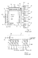
- FIG. 1 of the drawings A typical example of the semiconductor memory device is illustrated in figure 1 of the drawings, and the prior art semiconductor memory device comprises a regular memory cell array 1 accompanied with a row of redundant memory cells 1 a and columns of redundant memory cells 1 b. If a row of regular memory cells contains a defective memory cell, the defective row of regular memory cells is replaced with the row of redundant memory cells. On the other hand, if a defective memory cell is found in a column of regular memory cells, the defective column of regular memory cells and associated columns of regular memory cells are replaced with the columns of redundant memory cells.
- the prior art semiconductor memory device further comprises regular word lines WLO to WLm shared between the regular memory cell array 1 and the columns of redundant memory cells 1 b, a redundant word line RWL for replacing a row of regular memory cells with the row of redundant memory cells, a row address decoder/word line driver unit 2a coupled to the regular word lines WLO to WLm and a redundant word line driver unit 2b coupled to the redundant word line RWL instead of the regular word lines WLO to WLm.
- the row address decoder/word line driver unit When row address predecoded signals ADR are supplied to the row address decoder/ word line driver unit 2a, the row address decoder/word line driver unit activates one of the regular word lines WLO to WLm insofar as the row address predecoded signals does not indicate a row address assigned to the defective row of regular memory cells.
- the row address decoder/word line driver unit 2a maintains the regular word lines WLO to WLm in inactive level, and the redundant word line driver unit 2b activates the redundant word line RWL. Therefore, the regular word lines WLO to WLm and the row address decoder/word line driver unit 2a make a row of the regular memory cells and one of the redundant memory cells 1 b accessible.
- the prior art semiconductor memory device further comprises regular bit line pair groups BLO to BLn shared between the regular memory cell array 1 and the redundant memory cells 1 a, a redundant bit line pair group RBL coupled to the columns of redundant memory cells 1 b, a column address decoder/column selector unit 3a coupled between the regular bit line pair groups BLO to BLn and four data line pairs DL1, DL2, DL3 and DL4 and a redundant column selector unit 3b coupled between the redundant bit line pair group RBL and the data line pairs DL1 to DL4.
- the column address decoder/ column selector unit 3a couples the regular bit line group to the data line pairs DL1 to DL4. However, if the column address predecoded signals ADC selects the column address assigned to the defective bit line group, the column address decoder/column selector unit 3a isolates the data line pairs DL1 to DL4 from the regular bit line pair groups BLO to BLn, and the redundant bit line pair selector unit 3b connects the redundant bit line pair group to the data line pairs DL1 to DL4.
- the prior art semiconductor memory device further comprises four input/output data buffer circuits 4a, 4b, 4c and 4d coupled between the data line pairs DL1 to DL4 and input/output data pins P1, P2, P3 and P4, respectively.
- the data bits are transferred from either regular or redundant bit line pair group through the data line pairs DL1 to DL4 to the input/output data buffer circuits 4a to 4d, and the input/output data buffer circuits 4a to 4d supply a 4-bit output data signal to the input/output data pins P1 to P4.
- a 4-bit input data signal is supplied from the input/output data pins P1 to P4 to the input/output data buffer circuits 4a to 4d, and four write-in data bits are transferred from the input/output data buffer circuits 4a to 4d through the data line pairs DL1 to DL4 to the column address decoder/column selector unit 3a and the redundant column selector unit 3b.
- One of the column address decoder/column selector unit 3a and the redundant column selector unit 3b transfers the write-in data bits to one of the bit line pair groups BLO to BLn or the redundant bit line pair group RBL.
- Figure 2 illustrates a circuit configuration of the redundant word line driver unit 2b, and comprises a plurality of series combinations of fuse elements FSO/ FSCO/ FS1/ FSCO/ FSi/.../ FSCi and n-channel enhancement type switching transistors Qn1/ Qn2/ Qn3/ Qn4/.../Qni/ Qnj coupled between a positive power voltage line Vdd and a ground voltage line GND and a p-channel enhancement type charging transistor Qp1.
- the row address predecoded signals ARO/CARO/AR1 /CAR1 /ARi/CARi are respectively supplied to the gate electrodes of the n-channel enhancement type switching transistors Qn1 to Qnj, and a precharge control signal PC is supplied to the gate electrode of the p-channel enhancement type charging transistor Qp1.
- the fuse elements FSO to FSCi are selectively broken for storing the row address assigned to the defective row of regular memory cells.
- the circuit configuration shown in figure 2 is disclosed in Japanese patent Publication of Examined Application No. 63-10520.
- the fuse elements FSO, FSC1,... and FSi are broken by a laser beam, and the row address predecoded signals of logic "1" level are supplied to the gate electrodes of the n-channel enhancement type switching transistors associated with the broken fuse elements. If the stored row address is matched with the row address expressed by the row address predecoded signals ADR, no discharging path is provided from the p-channel enhancement type charging transistor Qp1 and the ground voltage line GND, and the p-channel enhancement type charging transistor Qp1 boosts the redundant word line RWL to the active high level.
- the row address expressed by the row address predecoded signals ADR is different from the stored address, current flows through at least one series combination of non-broken fuse element and the n-channel enhancement type switching transistor, and the redundant word line RWL is maintained in the inactive low level.
- the redundant bit line selecting unit 3b is similar to the redundant word line driving unit 3b.
- the row of redundant memory cells 1 a and the columns of redundant memory cells 1 b rescues a defective semiconductor memory device from rejection by replacing defective memory cells therewith, and the redundant facility enhances the production yield of the prior art semiconductor memory.
- the prior art redundant facility can not rescue the semiconductor memory device.
- Another rescuing technology is proposed in Japanese Patent Publication of Unexamined Application No. 61-17299, and an address buffer incorporated in the prior art semiconductor memory device disclosed therein prohibits a memory cell sub-array not rescued through replacement with redundant memory cells from a data access.
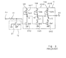
- Figure 3 illustrates the address buffer circuit 11 associated with a protective circuit 12 for an address pin An.
- the address pin An is coupled to a protective resistor R1, and the protective circuit 12 implemented by a field effect transistor Q1 is coupled between the resistor R1 and a ground voltage line GND.
- the address buffer circuit 11 comprises a three inverters INV1, INV2 and INV3 coupled between a positive power voltage line Vdd and the ground voltage line GND and two fuse elements F1 and F2, and the inverters INV1, INV2 and INV3 are implemented by depletion type/enhancement type field effect transistors Qd2/Qe3, Qd4/Qe5 and Qd6/Qe7.
- the fuse elements F1 and F2 are inserted between the depletion type field effect transistor Qd4 and the enhancement type field effect transistor Qe5 and between the depletion type field effect transistor Qd6 and the enhancement type field effect transistor Qe7, respectively.
- the gate electrodes of the depletion type field effect transistors Qd2, Qd4 and Qd6 are respectively connected to the output nodes N1, N2 and N3 of the inverters INV1 to INV3, and the resistor R1 and the output nodes N1 and N2 are respectively coupled to the gate electrodes of the enhancement type field effect transistors Qe3, Qe5 and Qe7 serving as input nodes of the inverters INV1 to INV3.
- the output node N3 serves as an output node of the address buffer circuit 1, and an address signal AO is supplied from the output node N3 to an addressing system (not shown).
- An external address bit supplied to the address pin An is indicative of either half of the memory cell array (not shown). If one of the halves of the memory cell arrays contains defective memory cells more than redundant memory cells, the manufacturer blows one of the fuse elements F1/F2, and fixes the address signal AO to one of the two levels.
- the fuse element F2 is broken, and the depletion type field effect transistor Qd6 fixes the address signal AO to the high level.
- the excellent half is accessed at all times regardless of the external address bit at the address pin An.
- the fuse element F1 is broken, and the other fuse element couples the output node N3 to the enhancement type field effect transistor Qe7.
- the positive high voltage level Vdd is supplied through the depletion type field effect transistor Qd4 regardless of the external address bit at the address pin An, and the enhancement type field effect transistor Qe7 is turned on at all times.
- the address signal AO is fixed to the low level, and the excellent half is accessed at all times.
- the broken fuse element decreases the memory capacity to a half of the original memory capacity, the manufacturer can sell the semiconductor memory device as a small data storage.
- any fuse elements F1 and F2 are never broken, and the address signal AO is changed depending upon the external address bit at the address pin An.
- the pair of fuse elements F1 and F2 are incorporated in each of the two address buffer circuits, and the manufacturer selectively prohibits the quarters of the memory cell array from data access.
- a manufacturer is, by way of example, assumed not to rescue one of the four memory cell sub-arrays forming a 16 mega-bit memory cells with the redundant memory cells, and prohibits the defective memory cell sub-array from a data access by blowing a fuse element incorporated in the address buffer circuit.
- the semiconductor memory device can be sold as a 12 mega-bit semiconductor memory device.
- the present invention proposes to provided a shifting circuit between data line pairs and data buffer circuits.
- a semiconductor memory device comprising: a) a memory cell array divided into a plurality of memory cell sub-arrays each implemented by a plurality of addressable memory cells for storing internal data bits, respectively; b) a plurality of data buffer circuits operative to change data bits between the internal data bits and external data bits, and having respective priorities different from one another; c) an addressing means operative to couple selected addressable memory cells respectively selected from the plurality of memory cell sub-arrays to the plurality of data buffer circuits; and d) a shifting circuit coupled between the addressing means and the plurality of data buffer circuits, and operative to respectively connect the plurality of memory cell sub-arrays to the data buffer circuits when a defective memory cell sub-array with a defective memory cell is not incorporated in the plurality of memory cell sub-arrays, the shifting circuit being further operative to connect available memory cell sub-arrays without the defective memory cell to the data buffer circuits in an order of the priority and to
- a semiconductor memory device embodying the present invention is fabricated on a semiconductor chip 21, and comprises a memory cell array 22 divided into four memory cell sub-arrays 22a to 22d.
- Each of the memory cell sub-arrays 22a to 22d has a plurality of regular memory cells arranged in rows and columns, a row of redundant memory cells 22e and a column of redundant memory cells 22f.
- the redundant memory cell is identical in circuit configuration with the regular memory cell, and small circles stand for some of the regular memory cells of the memory cell sub-array 22a. Data bits are respectively stored in the regular/redundant memory cells, and are rewritable.
- the semiconductor memory device further comprises a plurality of sets of regular and redundant word lines WLO to WLm and RWL respectively associated with the memory cell sub-arrays 22a to 22d and a plurality of sets of regular and redundant bit line pairs BLO, BL1,..., BLn and RBL also associated with the memory cell sub-arrays 22a to 22d, respectively.
- Row addresses are respectively assigned to the regular word lines WLO to WLm of each word line set, and column addresses are respectively assigned to the regular bit line pairs BLO to BLn.
- the regular word lines WLO to WLm are coupled to the respective rows of regular memory cells and the respective redundant memory cells 22f of the associated memory cell sub-array, and the redundant word line RWL is coupled to the associated row of redundant memory cells 22e.
- the regular bit line pairs BLO to BLn are coupled to the respective columns of regular memory cells and the respective redundant memory cells 22e, and the redundant bit line pair RBL is coupled to the associated column of the redundant memory cells 22f.
- a row of regular memory cells contains a defective memory cell not available for storing a data bit
- the defective row of regular memory cells is replaced with the row of redundant memory cells 22e.
- a column of regular memory cells contains a defective memory cell
- the defective column of regular memory cells is replaced with the column of redundant memory cells.
- the regular and/or redundant memory cells are coupled to the associated bit line pairs, and data bits are transferred between the regular and/or redundant memory cells and the associated bit line pairs, respectively.
- the semiconductor memory device further comprises a row selecting system 23 and a column selecting system 24, and the row selecting system 23 and the column selecting system 24 are coupled to the regular and redundant word lines WLO to WLm and RWL and the regular and redundant bit line pairs BLO to BLn and RBL.
- the row selecting system 23 has a decoder unit, a regular word line driver unit, a redundant circuit and a redundant word line driver unit.
- the decoder unit is responsive to row address predecoded signals ADR indicative of one of the row addresses for selecting one of the regular word lines WLO to WLm from each word line set, and the regular word line driver unit activates the selected regular word lines to the active level in the absence of a disable signal supplied from the redundant circuit.
- the redundant circuit stores the row addresses assigned to the defective rows of regular memory cells found in the respective memory cell sub-arrays 22a to 22d in a non-volatile manner, and the compares the row address represented by the row address predecoded signals ADR with the stored row addresses.
- the disable signal is not generated, and the regular word line driver unit activates the selected regular word lines.
- the redundant word line driver unit maintains the redundant word lines RWL to the inactive level.
- the redundant circuit supplies the disable signal to the regular word line driver unit for maintaining the selected regular word line to an inactive level, and causes the redundant word line driver to activate the redundant word line RWL to the active level instead of the selected regular word line.
- the other selected regular word lines are activated as usual.
- the column selecting system comprises a column address decoder unit responsive to column address predecoded signals ADC representing one of the column addresses, a regular column selector unit coupled between the sets of regular bit line pairs and four data line pairs DL1 to DL4, a redundant circuit and transfer gates respectively coupled to the redundant bit line pairs RBL and the four data line pairs DL1 to DL4.
- the four data line pairs are respectively associated with the four memory cell sub-arrays 22a to 22d, and the regular column selector unit and the transfer gates couples four regular/redundant bit line pairs respectively selected for the four memory cell sub-arrays 22a to 22d to the four data line pairs DL1 to DL4.
- the redundant circuit of the column selecting system stores column addresses respectively assigned to the defective columns of regular memory cells, and compares the column address represented by the column address predecoded signals with the stored column addresses for changing the defective bit line pairs to the associated redundant bit line pairs RBL.
- the redundant circuit disables the regular column selector unit not to couple the defective bit line pair with the associated data line pair, and the associated transfer gate couples the redundant bit line pair RBL to the associated data line pair.
- the regular column selector unit couples four regular bit line pairs respectively associated with the four memory cell sub-arrays 22a to 22d to the associated four data line pairs DL1 to DL4.
- the sets of regular and redundant word lines WLO to WLm and RWL, the sets of regular and redundant bit line pairs BLO to BLn and RBL, the row selecting system 23 and the column selecting system 24 as a whole constitute an addressing means.
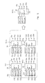
- the semiconductor memory device further comprises four input/output data buffer circuits 25a, 25b, 25c and 25d respectively coupled to data pins P1, P2, P3 and P4 and a shifting circuit 26 coupled between the four data line pairs DL1 to DL4 and the four input and output data buffer circuits 25a to 25d.
- the input and output data buffer circuits 25a to 25d generates an output data signal from potential differences on the data line pairs DL1 to DL4 in a read-out phase and potential difference from an input data signal in a write-in phase.
- the shifting circuit 26 comprises first blowable fuse elements F11, F12 and F13 respectively coupled between the data line pairs DL1, DL2 and DL3 and the input/output data buffer circuits 25a, 25b and 25c, second blowable fuse elements F21, F22 and F23 coupled between the data line pairs DL2, DL3 and DL4 and the input/output data buffer circuits 25a, 25b and 25c, an isolating circuit 26a coupled between the data line pair DL4 and the input/output data buffer circuit 25d and a gate control circuit 26b for controlling the isolating circuit 26a.
- the input/output data buffer circuits 25a, 25b and 25c have higher priority
- the input/output data buffer circuit 25d has lower priority.
- the fuse elements F11 to F13 and the fuse elements F21 to F23 form in combination a switching unit.
- the gate control circuit 26b comprises a series of a resistor R11 and a blowable fuse element F31 coupled between a positive power voltage line Vdd and a ground voltage line GND and a series of inverters INV41 and INV42 coupled to a node N11 between the resistor R11 and the blowable fuse element F31, and a gate control signal CTL and the complementary gate control signal CCTL are generated by the inverters INV41 and INV42, respectively.
- the fuse element F31 is much smaller in resistance than the resistor R11.
- the gate control signal CTL While the fuse element F31 is connecting the resistor R11 to the ground voltage line GND, the gate control signal CTL is maintained at a high level, and, accordingly, the complementary gate control signal CCTL remains at a low level. However, if the fuse element F31 is broken, the gate control signal CTL is changed to the low level, and, accordingly, the complementary gate control signal CCTL is elevated to the high level.
- the isolating circuit 26a comprises a transfer gate TG1 coupled between the data line pair DL4 and the input/output data buffer circuit 25d and a transfer gate TG2 coupled between the input/output data buffer circuit 25d and the ground voltage line GND.
- the transfer gates TG1 and TG2 are complementarily shifted between on-state and off-state, and couple the input/output data buffer circuit 25d with the lowest priority to the data line pair DL4 or the ground voltage line GND.
- the semiconductor memory device Upon completion of the fabrication process, the semiconductor memory device is subjected to a test sequence to see whether or not each of the memory cell sub-arrays 22a to 22d contains a defective memory cell not available for storing a data bit. If no defective memory cell is found in the memory cell sub-arrays 22a to 22d, the memory cell sub-arrays 22a to 22d are diagnosed as excellent memory cell sub-arrays.
- the defective row of regular memory cell and/or the defective column of regular memory cells are replaced with the row of redundant memory cells and/or the column of redundant memory cells, and the memory cell sub-array thus rescued through the redundant memory cells is also diagnosed to be the excellent memory cell sub-array.
- the redundant memory cells 22e and 22f can not rescue the memory cell sub-array, and the memory cell sub-array is diagnosed as a defective memory cell sub-array.
- the fuse element F31 is not broken, and the gate control signal CTL is maintained at the high level.
- the gate control signal CTL and the complementary gate control signal CCTL causes the transfer gate TG1 to connect the data line pair DL4 to the input/output data buffer circuit 25d, and the other transfer gate TG2 isolates the input/output data buffer circuit 25d from the ground voltage line GND.
- the shifting circuit 26 couples the four data bits to the four input/output data buffer circuits 25a to 25d, and potential differences are transferred between the input/output data buffer circuits 25a to 25d and the four regular/redundant bit line pairs associated with the selected four regular/redundant memory cells.
- the fuse element F31 is broken for changing the gate control signal CTL to the low level, and the fuse elements F11-F13 and F21 and F23 are selectively broken for changing the connection between the data line pairs DL1 to DL4 and the input/output data buffer circuits 25a to 25c.
- the shifting circuit connects the three excellent memory cell sub-arrays to the input/output data buffer circuits 25a to 25c in the order of priority.
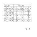
- Figure 6 illustrates broken fuse elements depending upon the defective memory cell sub-array, and the broken fuse elements are labeled with "B". If all of the memory cell sub-arrays 22a to 22d are excellent, the fuse elements F21, F22 and F23 are broken, and the other fuse elements provide signal paths. If the memory cell sub-array 22a is defective, the fuse element F31 is broken for disabling the input/output data buffer circuit 25d, and the fuse elements F11, F12 and F13 are broken instead of the fuse element F21, F22 and F23.
- the fuse elements F21, F12 and F13 are broken together with the fuse element F31.
- the defective memory cell sub-array 22c requires the broken fuse elements F21, F22, F13 and F31, and the fuse elements F21, F22, F23 and F31 are broken for the defective memory cell sub-array 22d.
- the shifting circuit 26 couples the excellent memory cell sub-arrays to the input/output data buffer circuits 25a, 25b and 25c at all times and the input/output data buffer circuit 25d to the ground voltage line GND regardless of the location of the defective memory cell sub-array.
- the manufacturer carries out test sequences through the input/output data buffer circuits 25a to 25c at all times, and a circuit board is shared between the rescued semiconductor memory device with partially excellent memory cell array 22.
- a shifting circuit 36 is connected between data line pairs DL1 to DL4 and input/output data buffer circuits incorporated in another semiconductor memory device embodying the present invention.
- the other components of the semiconductor memory device implementing the second embodiment are similar to those of the first embodiment, and are identified with the corresponding components of the first embodiment by using the same references in the following description.
- the shifting circuit 36 largely comprises an isolating circuit 36a for the input/output data buffer circuit 25d with the lower priority, a gate controlling circuit 36b for producing gate control signals and the complementary gate control signals and transfer gates TG11, TG12, TG13, TG21, TG22 and TG23, and the fuse elements F11, F12, F13, F21, F22 and F23 are replaced with the transfer gates TG11, TG12, TG13, TG21, TG22 and TG23, respectively.
- the isolating circuit 36a and the gate control circuit 36b behave as similar to the isolating circuit 26a and the gate control circuit 26b, and the transfer gates TG11 to TG23 are selectively turned on and off by the gate control circuit 26b depending upon the location of a defective memory cell sub-array.
- the transfer gates TG11 to TG13 and the transfer gates TG21 to TG23 as a whole constitute a switching unit.
- the isolating circuit 36a comprises a transfer gate TG31 coupled between the data line pair DL4 and the input/output data buffer circuit 25d and a transfer gate TG32 coupled between the input/output data buffer circuit 25d and the ground voltage line GND.
- the transfer gates TG31 and TG32 are complimentarily changed between on-state and off-state by a first gate control signal CTL10 and the complementary gate control signal CCTL10. Namely, if a defective memory cell sub-array is found through a test sequence, the first gate control signal CTL10 is fixed to the low level, and the first gate control signal CTL10 and the complementary gate control signal CCTL10 causes the transfer gate TG31 and the transfer gate TG32 to turn off and on. As a result, the input/output data buffer circuit 25d is isolated from the data line pair DL4, and is connected to the ground voltage line GND.
- the gate control circuit 36b comprises series of resistors R21/ R22/ R23/ R24 and fuse elements F41/F42/F43/F44 coupled between a positive power voltage line Vdd and the ground voltage line GND, a series of inverters INV51 and INV52 coupled to a node N21 between the resistor R21 and the fuse element F41 for producing the first gate control signal CTL10 and the complementary gate control signal CCTL10, a series of inverters INV53 and INV54 coupled to a node N22 between the resistor R22 and the fuse element F42 for producing a second gate control signal CTL11 and the complementary gate control signal CCTL11, a series of an inverter INV55, a NAND gate NA1 and inverters INV56 and INV57 coupled to a node N23 between the resistor R23 and the fuse element F43 for producing a third gate control signal CTL12 and the complementary gate control signal CCTL12 and a series of inverter INV58, a NAND
- the transfer gate TG31 connects the data line pair DL4 to the input/output data buffer circuit 25d, and the transfer gate TG32 blocks the input/output data buffer circuit 25d from the ground voltage line GND.
- the second to fourth gate control signals CTL11 to CTL13 cause transfer gates TG11 to TG13 to couple the data line pairs DL1 to DL3 to the input/output data buffer circuits 25a to 25c, and the transfer gates TG21 to TG23 are turned off.
- the shifting circuit 36 allows the semiconductor memory device to serves as a four-bit parallel input/output data storage.
- the fuse element F41 is broken for changing the first gate control signal CTL10 to the low level, and the transfer gate TG32 fixes the input/output data buffer circuit 25d to the ground voltage level.
- the fuse elements F42 to F44 are selectively broken depending upon the location of the defective memory cell sub-array, and the excellent memory cell sub-arrays are coupled through the shifting circuit 36 to the input/output data buffer circuits 25a to 25c, respectively.
- the shifting circuit according to the present invention couples the excellent memory cell sub-arrays to the input/output data buffer circuits with the higher priority, and the defective memory cell sub-array is electrically isolated from the input/output data buffer circuit with the lower priority.
- the input/output data buffer circuits with the higher priority are available at all times regardless of the location of the defective memory cell sub-array, and the semiconductor memory device according to the present invention is convenient for not only the manufacturer but also user.
- the present invention is applicable to a semiconductor memory device with more than four input/output data buffer circuits, and the isolating circuit may be provided for more than one input/output data buffer circuit.
- the fuse elements may be broken by using either laser beam or electric current, and the gate control circuit may be implemented by a built- in programmable read only memory circuit.
Landscapes
- For Increasing The Reliability Of Semiconductor Memories (AREA)
- Dram (AREA)
- Static Random-Access Memory (AREA)
Applications Claiming Priority (2)
| Application Number | Priority Date | Filing Date | Title |
|---|---|---|---|
| JP5296501A JPH07153296A (ja) | 1993-11-26 | 1993-11-26 | 半導体記憶装置 |
| JP296501/93 | 1993-11-26 |
Publications (2)
| Publication Number | Publication Date |
|---|---|
| EP0655687A1 true EP0655687A1 (de) | 1995-05-31 |
| EP0655687B1 EP0655687B1 (de) | 1999-01-27 |
Family
ID=17834372
Family Applications (1)
| Application Number | Title | Priority Date | Filing Date |
|---|---|---|---|
| EP94118367A Expired - Lifetime EP0655687B1 (de) | 1993-11-26 | 1994-11-22 | Halbleiter-Speicheranordnung mit Schieberschaltung, welche zwischen Datenbuslinien und Pufferschaltungen verbunden ist, zur Umsetzung von Verbindungen dazwischen |
Country Status (5)
| Country | Link |
|---|---|
| US (1) | US5465234A (de) |
| EP (1) | EP0655687B1 (de) |
| JP (1) | JPH07153296A (de) |
| KR (1) | KR0142036B1 (de) |
| DE (1) | DE69416267T2 (de) |
Cited By (1)
| Publication number | Priority date | Publication date | Assignee | Title |
|---|---|---|---|---|
| CN111413909A (zh) * | 2020-04-15 | 2020-07-14 | 联合华芯电子有限公司 | 基于机器人感知系统的神经元 |
Families Citing this family (22)
| Publication number | Priority date | Publication date | Assignee | Title |
|---|---|---|---|---|
| DE69024086T2 (de) | 1989-04-13 | 1996-06-20 | Sundisk Corp | EEprom-System mit Blocklöschung |
| JP3273440B2 (ja) * | 1994-10-19 | 2002-04-08 | マイクロン・テクノロジー・インコーポレーテッド | 部分的に良好なメモリ集積回路から使用可能な部分を得るための効率的な方法 |
| KR0157344B1 (ko) * | 1995-05-25 | 1998-12-01 | 김광호 | 반도체 메모리 장치의 퓨즈소자 회로 |
| US5619460A (en) * | 1995-06-07 | 1997-04-08 | International Business Machines Corporation | Method of testing a random access memory |
| US5668763A (en) * | 1996-02-26 | 1997-09-16 | Fujitsu Limited | Semiconductor memory for increasing the number of half good memories by selecting and using good memory blocks |
| JPH09282900A (ja) * | 1996-04-11 | 1997-10-31 | Oki Electric Ind Co Ltd | メモリモジュール |
| US5703500A (en) * | 1996-05-15 | 1997-12-30 | Micron Technology, Inc. | Threshold voltage scalable buffer with reference level |
| JPH1011969A (ja) * | 1996-06-21 | 1998-01-16 | Toshiba Microelectron Corp | 半導体記憶装置 |
| US5946257A (en) | 1996-07-24 | 1999-08-31 | Micron Technology, Inc. | Selective power distribution circuit for an integrated circuit |
| US5835425A (en) * | 1997-09-04 | 1998-11-10 | Siemens Aktiengesellschaft | Dimension programmable fusebanks and methods for making the same |
| US6332183B1 (en) | 1998-03-05 | 2001-12-18 | Micron Technology, Inc. | Method for recovery of useful areas of partially defective synchronous memory components |
| US6314527B1 (en) | 1998-03-05 | 2001-11-06 | Micron Technology, Inc. | Recovery of useful areas of partially defective synchronous memory components |
| US5963489A (en) * | 1998-03-24 | 1999-10-05 | International Business Machines Corporation | Method and apparatus for redundancy word line replacement in a repairable semiconductor memory device |
| US6381708B1 (en) | 1998-04-28 | 2002-04-30 | Micron Technology, Inc. | Method for decoding addresses for a defective memory array |
| US6381707B1 (en) | 1998-04-28 | 2002-04-30 | Micron Technology, Inc. | System for decoding addresses for a defective memory array |
| US6496876B1 (en) | 1998-12-21 | 2002-12-17 | Micron Technology, Inc. | System and method for storing a tag to identify a functional storage location in a memory device |
| US6578157B1 (en) | 2000-03-06 | 2003-06-10 | Micron Technology, Inc. | Method and apparatus for recovery of useful areas of partially defective direct rambus rimm components |
| US7269765B1 (en) | 2000-04-13 | 2007-09-11 | Micron Technology, Inc. | Method and apparatus for storing failing part locations in a module |
| US6909659B2 (en) * | 2001-08-30 | 2005-06-21 | Micron Technology, Inc. | Zero power chip standby mode |
| DE102004041731B3 (de) * | 2004-08-28 | 2006-03-16 | Infineon Technologies Ag | Speichermodul zum Bereitstellen einer Speicherkapazität |
| US7499352B2 (en) * | 2006-05-19 | 2009-03-03 | Innovative Silicon Isi Sa | Integrated circuit having memory array including row redundancy, and method of programming, controlling and/or operating same |
| WO2009008078A1 (ja) * | 2007-07-11 | 2009-01-15 | Fujitsu Microelectronics Limited | 半導体記憶装置及びシステム |
Citations (4)
| Publication number | Priority date | Publication date | Assignee | Title |
|---|---|---|---|---|
| JPS59168993A (ja) * | 1983-03-16 | 1984-09-22 | Hitachi Ltd | 半導体記憶装置 |
| EP0395612A2 (de) * | 1989-04-28 | 1990-10-31 | International Business Machines Corporation | Speichereinheit und Verfahren zur Herstellung derselben |
| EP0477809A2 (de) * | 1990-09-28 | 1992-04-01 | Intergraph Corporation | Sehr schnelle redundante Zeilen und Spalten für Halbleiter-Speicher |
| US5299160A (en) * | 1992-06-02 | 1994-03-29 | Mitsubishi Denki Kabushiki Kaisha | Semiconductor memory device capable of repairing defective bits |
Family Cites Families (6)
| Publication number | Priority date | Publication date | Assignee | Title |
|---|---|---|---|---|
| JPS58153293A (ja) * | 1982-03-05 | 1983-09-12 | Hitachi Ltd | 半導体メモリ |
| JPS6117299A (ja) * | 1984-07-04 | 1986-01-25 | Toshiba Corp | 半導体記憶装置 |
| JP2650895B2 (ja) * | 1986-07-02 | 1997-09-10 | 松下電器産業株式会社 | 露光装置および露光方法 |
| JPS6427099A (en) * | 1987-07-22 | 1989-01-30 | I O Data Kiki Kk | Semiconductor memory device |
| JPH05210998A (ja) * | 1992-01-30 | 1993-08-20 | Nec Corp | 半導体メモリ装置 |
| JPH05234394A (ja) * | 1992-02-21 | 1993-09-10 | Fujitsu Ltd | 冗長接続切換回路 |
-
1993
- 1993-11-26 JP JP5296501A patent/JPH07153296A/ja active Pending
-
1994
- 1994-11-22 DE DE69416267T patent/DE69416267T2/de not_active Expired - Fee Related
- 1994-11-22 EP EP94118367A patent/EP0655687B1/de not_active Expired - Lifetime
- 1994-11-23 US US08/347,078 patent/US5465234A/en not_active Expired - Fee Related
- 1994-11-26 KR KR1019940031362A patent/KR0142036B1/ko not_active Expired - Fee Related
Patent Citations (4)
| Publication number | Priority date | Publication date | Assignee | Title |
|---|---|---|---|---|
| JPS59168993A (ja) * | 1983-03-16 | 1984-09-22 | Hitachi Ltd | 半導体記憶装置 |
| EP0395612A2 (de) * | 1989-04-28 | 1990-10-31 | International Business Machines Corporation | Speichereinheit und Verfahren zur Herstellung derselben |
| EP0477809A2 (de) * | 1990-09-28 | 1992-04-01 | Intergraph Corporation | Sehr schnelle redundante Zeilen und Spalten für Halbleiter-Speicher |
| US5299160A (en) * | 1992-06-02 | 1994-03-29 | Mitsubishi Denki Kabushiki Kaisha | Semiconductor memory device capable of repairing defective bits |
Non-Patent Citations (3)
| Title |
|---|
| "HIGH PRODUCTIVITY MULTI-APPLICATION MEMORY CHIPS", IBM TECHNICAL DISCLOSURE BULLETIN, vol. 34, no. 4B, September 1991 (1991-09-01), NEW YORK US, pages 318 - 319, XP000189483 * |
| M. YOSHIDA ET AL.: "A 288K CMOS EPROM with Redundancy", IEEE JOURNAL OF SOLID-STATE CIRCUITS, vol. SC-18, no. 5, October 1983 (1983-10-01), NEW YORK US, pages 544 - 550 * |
| PATENT ABSTRACTS OF JAPAN vol. 9, no. 24 (P - 331) 31 January 1985 (1985-01-31) * |
Cited By (1)
| Publication number | Priority date | Publication date | Assignee | Title |
|---|---|---|---|---|
| CN111413909A (zh) * | 2020-04-15 | 2020-07-14 | 联合华芯电子有限公司 | 基于机器人感知系统的神经元 |
Also Published As
| Publication number | Publication date |
|---|---|
| DE69416267D1 (de) | 1999-03-11 |
| DE69416267T2 (de) | 1999-09-02 |
| JPH07153296A (ja) | 1995-06-16 |
| US5465234A (en) | 1995-11-07 |
| KR0142036B1 (ko) | 1998-07-15 |
| EP0655687B1 (de) | 1999-01-27 |
| KR950015390A (ko) | 1995-06-16 |
Similar Documents
| Publication | Publication Date | Title |
|---|---|---|
| US5465234A (en) | Semiconductor memory device having shifting circuit connected between data bus lines and data buffer circuits for changing connections therebetween | |
| US5243570A (en) | Semiconductor memory device having redundant memory cell columns concurrently accessible together with regular memory cell arrays | |
| US4837747A (en) | Redundary circuit with a spare main decoder responsive to an address of a defective cell in a selected cell block | |
| US6519192B2 (en) | Semiconductor memory device having a large band width and allowing efficient execution of redundant repair | |
| US4881200A (en) | Erasable programmable read only memory device | |
| US5548225A (en) | Block specific spare circuit | |
| US5563832A (en) | Semiconductor memory device having interface units memorizing available memory cell sub-arrays | |
| US4648075A (en) | Redundancy circuit for a semiconductor memory device | |
| US5485424A (en) | Semiconductor memory and redundant-address writing method | |
| EP0477809A2 (de) | Sehr schnelle redundante Zeilen und Spalten für Halbleiter-Speicher | |
| US5502676A (en) | Integrated circuit memory with column redundancy having shared read global data lines | |
| US5258953A (en) | Semiconductor memory device | |
| JP3631277B2 (ja) | メモリモジュール | |
| JPH03176899A (ja) | メモリ回路 | |
| CN100527275C (zh) | 按内容寻址的存储器器件 | |
| KR100325035B1 (ko) | 반도체 메모리 장치 | |
| KR0161343B1 (ko) | 용장메모리셀을 가지는 반도체기억장치 | |
| KR970012781A (ko) | 컬럼 리던던시 회로를 가지는 반도체 메모리 장치 | |
| US6804135B1 (en) | Content addressable memory having column redundancy | |
| US7016243B1 (en) | Content addressable memory having column redundancy | |
| KR970008445B1 (ko) | 반도체 기억 장치 | |
| US6545920B2 (en) | Defective address storage scheme for memory device | |
| US5848007A (en) | Redundancy circuit for semiconductor storage apparatus | |
| US6249466B1 (en) | Row redundancy scheme | |
| KR0166496B1 (ko) | 반도체 기억소자의 리던던시 장치 |
Legal Events
| Date | Code | Title | Description |
|---|---|---|---|
| PUAI | Public reference made under article 153(3) epc to a published international application that has entered the european phase |
Free format text: ORIGINAL CODE: 0009012 |
|
| 17P | Request for examination filed |
Effective date: 19950317 |
|
| AK | Designated contracting states |
Kind code of ref document: A1 Designated state(s): DE FR GB |
|
| 17Q | First examination report despatched |
Effective date: 19970115 |
|
| GRAG | Despatch of communication of intention to grant |
Free format text: ORIGINAL CODE: EPIDOS AGRA |
|
| GRAG | Despatch of communication of intention to grant |
Free format text: ORIGINAL CODE: EPIDOS AGRA |
|
| GRAH | Despatch of communication of intention to grant a patent |
Free format text: ORIGINAL CODE: EPIDOS IGRA |
|
| GRAH | Despatch of communication of intention to grant a patent |
Free format text: ORIGINAL CODE: EPIDOS IGRA |
|
| GRAH | Despatch of communication of intention to grant a patent |
Free format text: ORIGINAL CODE: EPIDOS IGRA |
|
| GRAA | (expected) grant |
Free format text: ORIGINAL CODE: 0009210 |
|
| AK | Designated contracting states |
Kind code of ref document: B1 Designated state(s): DE FR GB |
|
| REF | Corresponds to: |
Ref document number: 69416267 Country of ref document: DE Date of ref document: 19990311 |
|
| ET | Fr: translation filed | ||
| PLBE | No opposition filed within time limit |
Free format text: ORIGINAL CODE: 0009261 |
|
| STAA | Information on the status of an ep patent application or granted ep patent |
Free format text: STATUS: NO OPPOSITION FILED WITHIN TIME LIMIT |
|
| 26N | No opposition filed | ||
| PGFP | Annual fee paid to national office [announced via postgrant information from national office to epo] |
Ref country code: FR Payment date: 20011113 Year of fee payment: 8 |
|
| PGFP | Annual fee paid to national office [announced via postgrant information from national office to epo] |
Ref country code: GB Payment date: 20011121 Year of fee payment: 8 |
|
| PGFP | Annual fee paid to national office [announced via postgrant information from national office to epo] |
Ref country code: DE Payment date: 20011210 Year of fee payment: 8 |
|
| REG | Reference to a national code |
Ref country code: GB Ref legal event code: IF02 |
|
| PG25 | Lapsed in a contracting state [announced via postgrant information from national office to epo] |
Ref country code: GB Free format text: LAPSE BECAUSE OF NON-PAYMENT OF DUE FEES Effective date: 20021122 |
|
| PG25 | Lapsed in a contracting state [announced via postgrant information from national office to epo] |
Ref country code: DE Free format text: LAPSE BECAUSE OF NON-PAYMENT OF DUE FEES Effective date: 20030603 |
|
| GBPC | Gb: european patent ceased through non-payment of renewal fee | ||
| PG25 | Lapsed in a contracting state [announced via postgrant information from national office to epo] |
Ref country code: FR Free format text: LAPSE BECAUSE OF NON-PAYMENT OF DUE FEES Effective date: 20030731 |
|
| REG | Reference to a national code |
Ref country code: FR Ref legal event code: ST |