EP0656590A2 - Dispositif de mesure pour tester la connexion entre an moins deux assemblages - Google Patents
Dispositif de mesure pour tester la connexion entre an moins deux assemblages Download PDFInfo
- Publication number
- EP0656590A2 EP0656590A2 EP94203457A EP94203457A EP0656590A2 EP 0656590 A2 EP0656590 A2 EP 0656590A2 EP 94203457 A EP94203457 A EP 94203457A EP 94203457 A EP94203457 A EP 94203457A EP 0656590 A2 EP0656590 A2 EP 0656590A2
- Authority
- EP
- European Patent Office
- Prior art keywords
- test
- module
- signal
- arrangement
- input
- Prior art date
- Legal status (The legal status is an assumption and is not a legal conclusion. Google has not performed a legal analysis and makes no representation as to the accuracy of the status listed.)
- Granted
Links
- 238000012360 testing method Methods 0.000 title claims abstract description 191
- 230000008878 coupling Effects 0.000 claims abstract description 15
- 238000010168 coupling process Methods 0.000 claims abstract description 15
- 238000005859 coupling reaction Methods 0.000 claims abstract description 15
- 238000011156 evaluation Methods 0.000 claims description 9
- 230000000712 assembly Effects 0.000 description 6
- 238000000429 assembly Methods 0.000 description 6
- 238000005259 measurement Methods 0.000 description 2
- 238000000034 method Methods 0.000 description 2
- 238000010276 construction Methods 0.000 description 1
- 238000005516 engineering process Methods 0.000 description 1
Images
Classifications
-
- G—PHYSICS
- G01—MEASURING; TESTING
- G01R—MEASURING ELECTRIC VARIABLES; MEASURING MAGNETIC VARIABLES
- G01R31/00—Arrangements for testing electric properties; Arrangements for locating electric faults; Arrangements for electrical testing characterised by what is being tested not provided for elsewhere
- G01R31/28—Testing of electronic circuits, e.g. by signal tracer
- G01R31/317—Testing of digital circuits
- G01R31/3181—Functional testing
- G01R31/3185—Reconfiguring for testing, e.g. LSSD, partitioning
- G01R31/318533—Reconfiguring for testing, e.g. LSSD, partitioning using scanning techniques, e.g. LSSD, Boundary Scan, JTAG
- G01R31/318558—Addressing or selecting of subparts of the device under test
-
- G—PHYSICS
- G01—MEASURING; TESTING
- G01R—MEASURING ELECTRIC VARIABLES; MEASURING MAGNETIC VARIABLES
- G01R31/00—Arrangements for testing electric properties; Arrangements for locating electric faults; Arrangements for electrical testing characterised by what is being tested not provided for elsewhere
- G01R31/28—Testing of electronic circuits, e.g. by signal tracer
- G01R31/317—Testing of digital circuits
- G01R31/3181—Functional testing
- G01R31/3185—Reconfiguring for testing, e.g. LSSD, partitioning
- G01R31/318533—Reconfiguring for testing, e.g. LSSD, partitioning using scanning techniques, e.g. LSSD, Boundary Scan, JTAG
- G01R31/318536—Scan chain arrangements, e.g. connections, test bus, analog signals
Definitions
- the invention relates to a measuring device at least for testing the connections between at least two modules with a test arrangement for generating a test signal supplied to a test arrangement output and for evaluating an analysis signal supplied by a module, formed from the test signal and received at a test arrangement input.
- Such a measuring device is known, for example, from US Pat. No. 5,029,166, which contains a test arrangement for generating a test signal (TDI), a test clock signal (TCK) and a test control signal (TMS) and for receiving an analysis signal (TDO).
- TTI test signal
- TCK test clock signal
- TMS test control signal
- TDO analysis signal
- a boundary scan test is carried out by means of this measuring device.
- boundary scan cells are arranged in front of the inputs of the circuit arrangements to be tested, which cells receive either direct or derived test signals.
- a link between test signals and input signals can take place in the boundary scan cells.
- the boundary scan cells are connected in series and the last boundary scan cell emits an intermediate signal or an analysis signal.
- An analysis signal is given directly to the test arrangement.
- the intermediate signal is fed to the next boundary scan cell arrangement.
- connections of assemblies can be tested if the individual assemblies are connected together in a ring for the test or measurement. There is one Module test input connected to either a test arrangement output or a module test output of another module. If the connections of modules in a system are to be tested, all modules of the system must be available and functional. Such a ring configuration cannot be used in the construction of the system or in a modular system (for example in telecommunications technology) without further auxiliary measures.
- Another option is to use a star structure for testing components in a system. However, a separate control connection is required for each module for a test control signal assigned to each module.
- the invention is therefore based on the object of providing a measuring device which, in the case of modular systems, enables connections between the components of the system to be tested without great effort.
- the test arrangement is also provided for supplying a switching control signal to the control arrangement contained on an assembly, that a module contains a switching device controlled by the associated control arrangement, which is provided for forwarding a test signal or an intermediate signal formed from the test signal to a module test input and for receiving at least one further intermediate signal from a module test output, and that a switching device in one first switching state for coupling the module test input with the test arrangement output and the module test output with a Auxiliary connection and in a second switching state for coupling the module test input with an auxiliary connection and the module test output with the test arrangement input or with another auxiliary connection is provided.
- the modules to be tested or measured additionally contain a switching device which, in addition to a connection to the test arrangement, also has an auxiliary connection to at least one other module.
- the switching device is controlled by a control arrangement that is already present in complex assemblies, such as in telecommunications. The control is carried out as a function of the switching control signal.
- a switching device couples a module test input to the test arrangement output that supplies the test signal and the associated module test output to the auxiliary connection. If a switching device of a first assembly is in a first switching state, a switching device of a second assembly has a second switching state.
- the switching device of the second module couples its module test input to the auxiliary connection or to a further auxiliary connection if the connections of an intermediate, third module are also to be measured, and its module test output to the test arrangement input.
- the switching device of the third module establishes a coupling between the first auxiliary connection and the associated module test input on the one hand and a coupling between the second auxiliary connection and the module test output on the other hand. It would also be possible to add modules. Then further auxiliary connections would have to be made.
- the switching device changes to a third switching state.
- the module test input is coupled to the test arrangement output and the module test output is coupled to the test arrangement input.
- the switching device of a module that is not to be tested changes in a fourth switching state.
- the fourth switching state no coupling is provided between the module test input and the test arrangement output and between the module test output and the test arrangement input.
- the test arrangement contains a test generator and an evaluation circuit for generating a test signal and a test clock signal.
- the evaluation circuit generates a test control signal to be supplied to the modules and specifies a test process and evaluates an analysis signal.
- the test control signal indicates, for example, what type of test is to be carried out and how individual switching elements are to work on a module for carrying out the test.
- the switching device of a module which is controlled as a function of the switching control signal, is used in the first, second and third switching states to supply the test clock signal to the circuit arrangements of the module.
- control arrangements on a module also carry out other control processes in normal operation. Since such control arrangements are generally coupled to one another via a bus system, the evaluation circuit can be coupled to such a bus in a simple manner. The bus is therefore not only used to transmit a switching control signal.
- a new module can be inserted into the system in a simple manner if the test signal, the test clock signal, the test control signal and the intermediate signal are transmitted via lines arranged in a bus-like manner.
- the invention relates to a module which is used to receive a test signal to be supplied by a test arrangement via a test arrangement output or an intermediate signal from another module and to supply a further intermediate signal to a further module or one which is formed from the test signal and is to be supplied from a test arrangement input Analysis signal is provided.
- a control arrangement is arranged on the module for receiving a switching control signal from the test arrangement.
- a switching device controlled by the assigned control arrangement is also contained on the module, which is provided for forwarding a test signal or an intermediate signal formed from the test signal to a module test input and for receiving at least one further intermediate signal from a module test output.
- the switching device is in a first switching state for coupling the module test input to the test arrangement output and the module test output with an auxiliary connection and in a second switching state for coupling the module test input with an auxiliary connection and the module test output provided with the test arrangement input or with another auxiliary connection.
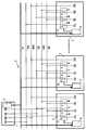
- FIG. 1 shows a measuring device for testing the connections between at least two modules and for testing a circuit arrangement on a module.
- the measuring device shown in the figure contains a test arrangement 1 with an evaluation circuit 2, which can be implemented, for example, as a microprocessor or signal processor, and a clock generator (not shown in more detail).
- an evaluation circuit 2 which can be implemented, for example, as a microprocessor or signal processor, and a clock generator (not shown in more detail).
- a boundary scan test of modules 3, 4 and 5 can be carried out.
- modules 3, 4 and 5 are supplied with a test clock signal TCK, a test control signal TMS and a test signal TDI from test arrangement 1. If the test signal, which is generated, for example, in the test arrangement 1, has passed through one or more modules 3, 4 and 5, an analysis signal TDO is received, which is evaluated by the evaluation circuit 2 and indicates whether the system or the modules are working correctly.
- the test signal TDI can deliver a test sequence which is fed directly to the individual boundary scan cells in a module 3, 4 or 5 or a circuit arrangement on the module 3, 4 or 5 or in a converter circuit on a module 3, 4 or 5 is implemented.
- the test control signal TMS indicates, for example, which test it is.
- the test arrangement 1 is coupled to the modules 3, 4 and 5 via a bus system 6.
- Each assembly 3, 4 and 5 contains, in addition to the circuit arrangements provided for specific functions of the assembly Switching device 7, 8 and 9.
- This switching device is controlled by a control arrangement 10, 11 and 12, which also performs other functions on the assembly 3, 4 and 5 in normal operation and is designed, for example, as a microprocessor or signal processor.
- the control arrangements 10, 11 and 12 are coupled to one another and to the evaluation circuit 2 via lines ST of the bus system 6.
- a control signal from the evaluation circuit 2 is supplied to the control arrangements 10, 11 and 12 via the lines ST of the bus system 6.
- the bus system 6 also contains a line BCK on which the test clock signal TCK is transmitted.
- the test control signal TMS is applied to a line BMS of the bus system 6.
- the test signal TDI is fed to a line BDI and the analysis signal TDO to a line BDO of the bus system 6.
- An auxiliary line BR is also present in the bus system 6, which enables at least one auxiliary connection between two modules.
- the switching device 7 contains three individual switches 13, 14 and 15, which forward signals supplied to the module 3 via the bus system 6.
- the first switch 13 in the switching device 7 can establish a connection with the bus line BCK or go into a rest position. If the switch 13 is not in an idle position, it forwards the test clock signal TCK to circuit arrangements of module 3.
- the second switch 14 in the switching device 7 serves to establish a connection either between the bus line BDI or the auxiliary line BR. This switch 14 can also go into a rest position in which there is no connection to a bus line.
- the switch 14 If the switch 14 is not in a rest position, it delivers a module test input of module 3 either a test signal TDI from a test arrangement output of test arrangement 1 or receives a derived test signal from another module 4 or 5 via the auxiliary line BR of the bus system 6.
- the switch 15 can connect to the bus line BDO and a connection with the auxiliary line BR.
- the switch 15 also has a rest position.
- a test signal that has passed through circuit arrangements of module 3, for example, is routed via a module test output of module 3 via switch 15 to auxiliary line BR of bus system 6 or via bus line BDO to the test arrangement input of test arrangement 1.
- the switching devices 8 and 9 also each have three switches 16, 17 and 18 or 19, 20 and 21. These switches 16, 17 and 18 or 19, 20 and 21 operate in the same way as the switches 13, 14 and 15 of the switching device 7.
- the switch 13 forwards the clock signal to one or more circuit arrangements of the module 3, 4 or 5.
- the switch 14 supplies, for example, a test signal TDI via the bus line BDI to the module test input of the module 3.
- the test signal passing through the module 3 is passed as an analysis signal via the switch 15 of the switching device 7 to the bus line BDO.
- the switching device is in a third switching state.
- the other switches 16, 17 and 18 or 19, 20 and 21 of the switching devices 8 and 9 are in a rest position (fourth switching state).
- module 3 When testing or measuring connections between two modules, for example modules 3 and 4, module 3 receives test signal TDI via switch 14, for example.
- the test signal passing through the module is given as an intermediate signal via the switch 15 of the switching device 7 to the auxiliary line BR of the bus system 6.
- the switching device 7 is in a first switching state in this case.
- the switch 17 of the test device 8 (module 4) conducts the intermediate signal from the auxiliary line BR to the module test input of the module 4.
- This intermediate signal passing through the various circuit arrangements of the module 4 is given as an analysis signal via the switch 18 of the switching device 8 to the bus line BDO and after Reception evaluated in the test generator 1.
- the switching device 8 is in a second switching state.
- the switches 19, 20 and 21 of the other switching device 9 are in the rest position (fourth switching state).
- test clock signal TCK is only led to circuit arrangements of modules 3, 4 and 5 in the fourth switching state.
- test control signal TMS has a direct connection to circuit arrangements of modules 3, 4 and 5.
Landscapes
- Engineering & Computer Science (AREA)
- General Engineering & Computer Science (AREA)
- Physics & Mathematics (AREA)
- General Physics & Mathematics (AREA)
- Tests Of Electronic Circuits (AREA)
- Test And Diagnosis Of Digital Computers (AREA)
- Monitoring And Testing Of Transmission In General (AREA)
- Testing Of Short-Circuits, Discontinuities, Leakage, Or Incorrect Line Connections (AREA)
- Testing Electric Properties And Detecting Electric Faults (AREA)
Applications Claiming Priority (2)
| Application Number | Priority Date | Filing Date | Title |
|---|---|---|---|
| DE4340899 | 1993-12-01 | ||
| DE4340899A DE4340899A1 (de) | 1993-12-01 | 1993-12-01 | Meßvorrichtung zum Testen der Verbindungen zwischen wenigstens zwei Baugruppen |
Publications (3)
| Publication Number | Publication Date |
|---|---|
| EP0656590A2 true EP0656590A2 (fr) | 1995-06-07 |
| EP0656590A3 EP0656590A3 (fr) | 1997-11-19 |
| EP0656590B1 EP0656590B1 (fr) | 2002-02-13 |
Family
ID=6503888
Family Applications (1)
| Application Number | Title | Priority Date | Filing Date |
|---|---|---|---|
| EP94203457A Expired - Lifetime EP0656590B1 (fr) | 1993-12-01 | 1994-11-29 | Dispositif de mesure pour tester la connexion entre an moins deux sous-groupes |
Country Status (4)
| Country | Link |
|---|---|
| US (1) | US5581565A (fr) |
| EP (1) | EP0656590B1 (fr) |
| JP (1) | JP3756209B2 (fr) |
| DE (2) | DE4340899A1 (fr) |
Families Citing this family (5)
| Publication number | Priority date | Publication date | Assignee | Title |
|---|---|---|---|---|
| US5796938A (en) * | 1996-12-11 | 1998-08-18 | International Business Machines Corporation | Diagnostic subsystem and method for SCSI Interface |
| US6425101B1 (en) | 1998-10-30 | 2002-07-23 | Infineon Technologies North America Corp. | Programmable JTAG network architecture to support proprietary debug protocol |
| JP2003520967A (ja) * | 2000-01-21 | 2003-07-08 | サン・マイクロシステムズ・インコーポレイテッド | 構成可能なバウンダリ・スキャン・パスを有するプリント回路アセンブリ |
| ES2187279B1 (es) * | 2001-06-27 | 2004-09-01 | Aplicacions Tecnologiques Per Al Control De Qualitat, S.L. | Sistema para la comprobacion de cableados. |
| US7340659B2 (en) * | 2002-05-15 | 2008-03-04 | Infineon Technologies, A.G. | Method of testing multiple modules on an integrated circuit |
Family Cites Families (6)
| Publication number | Priority date | Publication date | Assignee | Title |
|---|---|---|---|---|
| US4860290A (en) * | 1987-06-02 | 1989-08-22 | Texas Instruments Incorporated | Logic circuit having individually testable logic modules |
| US5155432A (en) * | 1987-10-07 | 1992-10-13 | Xilinx, Inc. | System for scan testing of logic circuit networks |
| JPH0758319B2 (ja) * | 1989-02-07 | 1995-06-21 | 株式会社東芝 | テスト容易化回路 |
| US5029166A (en) * | 1989-05-31 | 1991-07-02 | At&T Bell Laboratories | Method and apparatus for testing circuit boards |
| JP2561164B2 (ja) * | 1990-02-26 | 1996-12-04 | 三菱電機株式会社 | 半導体集積回路 |
| DE4037687A1 (de) * | 1990-11-27 | 1992-06-04 | Standard Elektrik Lorenz Ag | Einrichtung zur pruefung von baugruppen in digitalen elektronischen systemen |
-
1993
- 1993-12-01 DE DE4340899A patent/DE4340899A1/de not_active Withdrawn
-
1994
- 1994-11-29 DE DE59410048T patent/DE59410048D1/de not_active Expired - Fee Related
- 1994-11-29 EP EP94203457A patent/EP0656590B1/fr not_active Expired - Lifetime
- 1994-11-30 JP JP29709794A patent/JP3756209B2/ja not_active Expired - Fee Related
- 1994-12-01 US US08/349,094 patent/US5581565A/en not_active Expired - Lifetime
Also Published As
| Publication number | Publication date |
|---|---|
| US5581565A (en) | 1996-12-03 |
| DE4340899A1 (de) | 1995-06-08 |
| JPH07264106A (ja) | 1995-10-13 |
| EP0656590B1 (fr) | 2002-02-13 |
| EP0656590A3 (fr) | 1997-11-19 |
| JP3756209B2 (ja) | 2006-03-15 |
| DE59410048D1 (de) | 2002-03-21 |
Similar Documents
| Publication | Publication Date | Title |
|---|---|---|
| DE3130714C2 (fr) | ||
| DE69003891T2 (de) | Testvorrichtung für gedruckte Schaltungskarten und ihre Anwendung für das Testen von gedruckten Schaltungskarten, in Form einer Multiplex-Demultiplexeinrichtung für numerische Signale. | |
| EP0009572A2 (fr) | Méthode et dispositif pour le test de circuits séquentiels réalisés en circuits semi-conducteurs qui sont monolithiquement intégrés | |
| EP1065509A2 (fr) | Dispositif diagnostique pour système à plusieurs antennes | |
| DE10256623A1 (de) | Elektrisches Gerät und Verfahren zum Betreiben eines elektrischen Geräts | |
| DE19536226A1 (de) | Testbare Schaltungsanordnung mit mehreren identischen Schaltungsblöcken | |
| DE3727549C2 (fr) | ||
| EP0656590B1 (fr) | Dispositif de mesure pour tester la connexion entre an moins deux sous-groupes | |
| EP0176863A1 (fr) | Audiomètre | |
| EP0024045A1 (fr) | Dispositif de vérification pour le diagnostic d'erreurs dans des systèmes de multicalculateurs, en particulier dans des systèmes multimicroprocesseurs | |
| DE69802976T2 (de) | Vorrichtung zum Messen des Gehalts an gelöstem Sauerstoff und des pH-Wertes einer Probe | |
| EP0265837A2 (fr) | Montage de circuit, son application et procédé de contrôle pour un réseau de communication de messages | |
| DE19832307C2 (de) | Integrierte Schaltung mit einer Selbsttesteinrichtung | |
| DE3936988C2 (fr) | ||
| EP0354214B1 (fr) | Procede de determination de la duree electrique de trajets de signaux | |
| DE69404043T2 (de) | Vorrichtung zum elektrischen prüfen eines elements einer elektrichen verbindung | |
| DE69709329T2 (de) | Modul mit schnittstelle zur prüfung und diagnose einer elektronischen telekommunikationseinrichtung | |
| EP0733910B1 (fr) | Circuit imprime avec test des connections incorporé pour des circuits intégrés | |
| DE3923764C1 (fr) | ||
| EP0037965A2 (fr) | Dispositif pour essayer un circuit digital avec des circuits d'essai insérés dans ce circuit | |
| DE69433618T2 (de) | Gerät zur prüfung der verbindung zwischen dem ausgang einer schaltung mit fester logischer ausgabe und dem eingang eines weiteren schaltkreises | |
| DE3689245T2 (de) | Automatische Prüfvorrichtung. | |
| EP0458300A2 (fr) | Test de fonctions de parties d'actionnement commandées par calculateur dans un véhicule | |
| DE69119140T2 (de) | Mit integrierten Schaltungen versehene Prüfvorrichtung für eine gedruckte Schaltung und Anwendung dieser Vorrichtung zum Prüfen einer solchen gedruckten Schaltung | |
| DE2511923C3 (de) | Schaltungsanordnung zur Funktionsprüfung und Fehlerlokalisierung von Flachbangruppen |
Legal Events
| Date | Code | Title | Description |
|---|---|---|---|
| PUAI | Public reference made under article 153(3) epc to a published international application that has entered the european phase |
Free format text: ORIGINAL CODE: 0009012 |
|
| AK | Designated contracting states |
Kind code of ref document: A2 Designated state(s): DE FR GB |
|
| PUAL | Search report despatched |
Free format text: ORIGINAL CODE: 0009013 |
|
| AK | Designated contracting states |
Kind code of ref document: A3 Designated state(s): DE FR GB |
|
| 17P | Request for examination filed |
Effective date: 19980519 |
|
| 17Q | First examination report despatched |
Effective date: 19991122 |
|
| RAP3 | Party data changed (applicant data changed or rights of an application transferred) |
Owner name: KONINKLIJKE PHILIPS ELECTRONICS N.V. Owner name: PHILIPS CORPORATE INTELLECTUAL PROPERTY GMBH |
|
| GRAG | Despatch of communication of intention to grant |
Free format text: ORIGINAL CODE: EPIDOS AGRA |
|
| RIC1 | Information provided on ipc code assigned before grant |
Free format text: 7G 06F 11/267 A, 7G 01R 31/04 B, 7G 01R 31/3185 B |
|
| GRAG | Despatch of communication of intention to grant |
Free format text: ORIGINAL CODE: EPIDOS AGRA |
|
| GRAH | Despatch of communication of intention to grant a patent |
Free format text: ORIGINAL CODE: EPIDOS IGRA |
|
| GRAH | Despatch of communication of intention to grant a patent |
Free format text: ORIGINAL CODE: EPIDOS IGRA |
|
| GRAA | (expected) grant |
Free format text: ORIGINAL CODE: 0009210 |
|
| REG | Reference to a national code |
Ref country code: GB Ref legal event code: IF02 |
|
| AK | Designated contracting states |
Kind code of ref document: B1 Designated state(s): DE FR GB |
|
| REF | Corresponds to: |
Ref document number: 59410048 Country of ref document: DE Date of ref document: 20020321 |
|
| GBT | Gb: translation of ep patent filed (gb section 77(6)(a)/1977) |
Effective date: 20020412 |
|
| ET | Fr: translation filed | ||
| RAP2 | Party data changed (patent owner data changed or rights of a patent transferred) |
Owner name: KONINKLIJKE PHILIPS ELECTRONICS N.V. Owner name: PHILIPS CORPORATE INTELLECTUAL PROPERTY GMBH |
|
| REG | Reference to a national code |
Ref country code: GB Ref legal event code: 746 Effective date: 20020917 |
|
| REG | Reference to a national code |
Ref country code: FR Ref legal event code: D6 |
|
| PLBE | No opposition filed within time limit |
Free format text: ORIGINAL CODE: 0009261 |
|
| STAA | Information on the status of an ep patent application or granted ep patent |
Free format text: STATUS: NO OPPOSITION FILED WITHIN TIME LIMIT |
|
| 26N | No opposition filed |
Effective date: 20021114 |
|
| PGFP | Annual fee paid to national office [announced via postgrant information from national office to epo] |
Ref country code: DE Payment date: 20060117 Year of fee payment: 12 |
|
| PG25 | Lapsed in a contracting state [announced via postgrant information from national office to epo] |
Ref country code: DE Free format text: LAPSE BECAUSE OF NON-PAYMENT OF DUE FEES Effective date: 20070601 |
|
| PGFP | Annual fee paid to national office [announced via postgrant information from national office to epo] |
Ref country code: FR Payment date: 20081125 Year of fee payment: 15 |
|
| PGFP | Annual fee paid to national office [announced via postgrant information from national office to epo] |
Ref country code: GB Payment date: 20081211 Year of fee payment: 15 |
|
| GBPC | Gb: european patent ceased through non-payment of renewal fee |
Effective date: 20091129 |
|
| REG | Reference to a national code |
Ref country code: FR Ref legal event code: ST Effective date: 20100730 |
|
| PG25 | Lapsed in a contracting state [announced via postgrant information from national office to epo] |
Ref country code: FR Free format text: LAPSE BECAUSE OF NON-PAYMENT OF DUE FEES Effective date: 20091130 |
|
| PG25 | Lapsed in a contracting state [announced via postgrant information from national office to epo] |
Ref country code: GB Free format text: LAPSE BECAUSE OF NON-PAYMENT OF DUE FEES Effective date: 20091129 |