EP0656647A1 - Verfahren zur Herstellung einer integrierten Schaltungsanordnung mit mindestens einem MOS-Transistor - Google Patents
Verfahren zur Herstellung einer integrierten Schaltungsanordnung mit mindestens einem MOS-Transistor Download PDFInfo
- Publication number
- EP0656647A1 EP0656647A1 EP94117699A EP94117699A EP0656647A1 EP 0656647 A1 EP0656647 A1 EP 0656647A1 EP 94117699 A EP94117699 A EP 94117699A EP 94117699 A EP94117699 A EP 94117699A EP 0656647 A1 EP0656647 A1 EP 0656647A1
- Authority
- EP
- European Patent Office
- Prior art keywords
- layer
- doped
- grown
- opening
- conductivity type
- Prior art date
- Legal status (The legal status is an assumption and is not a legal conclusion. Google has not performed a legal analysis and makes no representation as to the accuracy of the status listed.)
- Granted
Links
Images


Classifications
-
- H—ELECTRICITY
- H10—SEMICONDUCTOR DEVICES; ELECTRIC SOLID-STATE DEVICES NOT OTHERWISE PROVIDED FOR
- H10D—INORGANIC ELECTRIC SEMICONDUCTOR DEVICES
- H10D30/00—Field-effect transistors [FET]
- H10D30/01—Manufacture or treatment
- H10D30/021—Manufacture or treatment of FETs having insulated gates [IGFET]
- H10D30/025—Manufacture or treatment of FETs having insulated gates [IGFET] of vertical IGFETs
-
- H—ELECTRICITY
- H10—SEMICONDUCTOR DEVICES; ELECTRIC SOLID-STATE DEVICES NOT OTHERWISE PROVIDED FOR
- H10D—INORGANIC ELECTRIC SEMICONDUCTOR DEVICES
- H10D30/00—Field-effect transistors [FET]
- H10D30/01—Manufacture or treatment
- H10D30/021—Manufacture or treatment of FETs having insulated gates [IGFET]
- H10D30/0223—Manufacture or treatment of FETs having insulated gates [IGFET] having source and drain regions or source and drain extensions self-aligned to sides of the gate
- H10D30/0227—Manufacture or treatment of FETs having insulated gates [IGFET] having source and drain regions or source and drain extensions self-aligned to sides of the gate having both lightly-doped source and drain extensions and source and drain regions self-aligned to the sides of the gate, e.g. lightly-doped drain [LDD] MOSFET or double-diffused drain [DDD] MOSFET
-
- H—ELECTRICITY
- H10—SEMICONDUCTOR DEVICES; ELECTRIC SOLID-STATE DEVICES NOT OTHERWISE PROVIDED FOR
- H10D—INORGANIC ELECTRIC SEMICONDUCTOR DEVICES
- H10D30/00—Field-effect transistors [FET]
- H10D30/60—Insulated-gate field-effect transistors [IGFET]
- H10D30/63—Vertical IGFETs
-
- H—ELECTRICITY
- H10—SEMICONDUCTOR DEVICES; ELECTRIC SOLID-STATE DEVICES NOT OTHERWISE PROVIDED FOR
- H10D—INORGANIC ELECTRIC SEMICONDUCTOR DEVICES
- H10D84/00—Integrated devices formed in or on semiconductor substrates that comprise only semiconducting layers, e.g. on Si wafers or on GaAs-on-Si wafers
- H10D84/80—Integrated devices formed in or on semiconductor substrates that comprise only semiconducting layers, e.g. on Si wafers or on GaAs-on-Si wafers characterised by the integration of at least one component covered by groups H10D12/00 or H10D30/00, e.g. integration of IGFETs
- H10D84/82—Integrated devices formed in or on semiconductor substrates that comprise only semiconducting layers, e.g. on Si wafers or on GaAs-on-Si wafers characterised by the integration of at least one component covered by groups H10D12/00 or H10D30/00, e.g. integration of IGFETs of only field-effect components
- H10D84/83—Integrated devices formed in or on semiconductor substrates that comprise only semiconducting layers, e.g. on Si wafers or on GaAs-on-Si wafers characterised by the integration of at least one component covered by groups H10D12/00 or H10D30/00, e.g. integration of IGFETs of only field-effect components of only insulated-gate FETs [IGFET]
- H10D84/837—Integrated devices formed in or on semiconductor substrates that comprise only semiconducting layers, e.g. on Si wafers or on GaAs-on-Si wafers characterised by the integration of at least one component covered by groups H10D12/00 or H10D30/00, e.g. integration of IGFETs of only field-effect components of only insulated-gate FETs [IGFET] comprising vertical IGFETs
-
- H—ELECTRICITY
- H10—SEMICONDUCTOR DEVICES; ELECTRIC SOLID-STATE DEVICES NOT OTHERWISE PROVIDED FOR
- H10D—INORGANIC ELECTRIC SEMICONDUCTOR DEVICES
- H10D84/00—Integrated devices formed in or on semiconductor substrates that comprise only semiconducting layers, e.g. on Si wafers or on GaAs-on-Si wafers
- H10D84/80—Integrated devices formed in or on semiconductor substrates that comprise only semiconducting layers, e.g. on Si wafers or on GaAs-on-Si wafers characterised by the integration of at least one component covered by groups H10D12/00 or H10D30/00, e.g. integration of IGFETs
- H10D84/82—Integrated devices formed in or on semiconductor substrates that comprise only semiconducting layers, e.g. on Si wafers or on GaAs-on-Si wafers characterised by the integration of at least one component covered by groups H10D12/00 or H10D30/00, e.g. integration of IGFETs of only field-effect components
- H10D84/83—Integrated devices formed in or on semiconductor substrates that comprise only semiconducting layers, e.g. on Si wafers or on GaAs-on-Si wafers characterised by the integration of at least one component covered by groups H10D12/00 or H10D30/00, e.g. integration of IGFETs of only field-effect components of only insulated-gate FETs [IGFET]
- H10D84/85—Complementary IGFETs, e.g. CMOS
-
- H—ELECTRICITY
- H10—SEMICONDUCTOR DEVICES; ELECTRIC SOLID-STATE DEVICES NOT OTHERWISE PROVIDED FOR
- H10P—GENERIC PROCESSES OR APPARATUS FOR THE MANUFACTURE OR TREATMENT OF DEVICES COVERED BY CLASS H10
- H10P14/00—Formation of materials, e.g. in the shape of layers or pillars
- H10P14/20—Formation of materials, e.g. in the shape of layers or pillars of semiconductor materials
- H10P14/24—Formation of materials, e.g. in the shape of layers or pillars of semiconductor materials using chemical vapour deposition [CVD]
-
- H—ELECTRICITY
- H10—SEMICONDUCTOR DEVICES; ELECTRIC SOLID-STATE DEVICES NOT OTHERWISE PROVIDED FOR
- H10P—GENERIC PROCESSES OR APPARATUS FOR THE MANUFACTURE OR TREATMENT OF DEVICES COVERED BY CLASS H10
- H10P95/00—Generic processes or apparatus for manufacture or treatments not covered by the other groups of this subclass
- H10P95/90—Thermal treatments, e.g. annealing or sintering
-
- H—ELECTRICITY
- H10—SEMICONDUCTOR DEVICES; ELECTRIC SOLID-STATE DEVICES NOT OTHERWISE PROVIDED FOR
- H10D—INORGANIC ELECTRIC SEMICONDUCTOR DEVICES
- H10D64/00—Electrodes of devices having potential barriers
- H10D64/20—Electrodes characterised by their shapes, relative sizes or dispositions
- H10D64/27—Electrodes not carrying the current to be rectified, amplified, oscillated or switched, e.g. gates
- H10D64/311—Gate electrodes for field-effect devices
- H10D64/411—Gate electrodes for field-effect devices for FETs
- H10D64/511—Gate electrodes for field-effect devices for FETs for IGFETs
- H10D64/514—Gate electrodes for field-effect devices for FETs for IGFETs characterised by the insulating layers
- H10D64/516—Gate electrodes for field-effect devices for FETs for IGFETs characterised by the insulating layers the thicknesses being non-uniform
Definitions
- CMOS transistors and logic gates are currently mostly implemented using planar silicon technology in which the source, channel region and drain are arranged laterally.
- the gate lengths that can be achieved depend on the resolving power of the optical lithography used and on tolerances in the structuring and adjustment. Typical gate lengths of 0.6 ⁇ m are achieved in the 16 M generation and 0.35 ⁇ m in the 64 M generation.
- MOS transistors With regard to the electrical properties of MOS transistors as well as to an increased packing density, which is particularly important in complex logic circuits such as logic gates, since several n- and p-channel transistors have to be additionally insulated from one another and wired to one another, there is a further reduction of the lateral channel lengths. This requires improvements in optical lithography and in the coating and etching technology. Due to the limited resolving power of optical lithography and increasing problems with tolerances in the structuring and adjustment, it seems questionable whether transistors with channel lengths below 100 nm can be reproducibly produced in this way. In addition, the reduction in the lateral channel length leads to changes in the electrical properties of the MOS transistor, which must be compensated for by implantation of dopants in the channel region and complex source / drain designs.
- Texas Instruments proposed that the transistor and capacitor be vertically integrated in the so-called "trench transistor cell" .
- the transistor proposed there has a channel length in the range of approximately 1 ⁇ m.
- the invention is based on the problem of specifying a production method for MOS transistors with a defined channel length in the range below 50 nm.
- the method is said to be particularly suitable for producing compact, fast logic gates.
- a source connection region is generated on a main surface of a substrate.
- a silicon wafer is used as the substrate.
- the source connection region can be formed on the main surface of the silicon wafer both as a continuous, correspondingly doped layer and as a doped trough.
- an SOI substrate can also be used as the substrate.
- the source connection region is realized in the single-crystal silicon layer. To achieve maximum packing density, it is surrounded by an insulating trench.
- an insulating layer is applied to the entire surface of the main area, in which a first opening is created.
- the surface for the later source area is exposed within the first opening.
- Epitaxial growth of doped semiconductor material produces a vertical layer sequence in the first opening, which comprises at least one channel region and a drain region and preferably additionally a source region for the MOS transistor. If the layer sequence only includes the channel area and the drain area, the source connection area also acts as a source area.
- the layer sequence is preferably produced by molecular beam epitaxy, with which particularly thin layers can be produced, or by selective epitaxy, in particular in an RTP-CVD process with SiH 2 Cl 2 gas, a corresponding doping gas being added in each case for in-situ doping.
- a non-selective method is used to grow the layer sequence, then semiconductor material grows both on the surface of the source connection region and on the surface of the insulating layer. The semiconductor material grows single-crystal on the surface of the source connection region, but polycrystalline on the surface of the insulating layer. The polycrystalline semiconductor material can then be selectively removed for the single-crystalline layer structure.
- the use of a selective epitaxy method has the advantage that this etching step is omitted.
- a second opening is then created in the layer sequence, which is at least as deep as it corresponds to the sum of the thicknesses of the drain region and channel region and, if appropriate, additionally of the source region.
- a gate dielectric and a gate electrode are grown on the surface of the second opening.
- MOS transistor produced in this way, it forms along the surface of the second opening a conductive channel in the channel area. Since the second opening is arranged in the interior of the layer structure, where the crystal structure is essentially defect-free, MOS transistors with good electrical properties can be produced in the method according to the invention.
- the manufacturing method according to the invention is suitable for constructing an inverter which comprises two transistors which are complementary to one another. For this purpose, layer sequences with corresponding doping are grown in the first opening.
- Layers which form source / drain regions in the circuit are heavily doped and deposited in a thickness of 50 to 200 nm.
- Layers which form channel regions in the circuit are less heavily doped with dopant concentrations in the range 1017 to 1018 cm ⁇ 3 and are deposited in a thickness of 10 to 200 nm, preferably 50 to 100 nm. The thickness of these layers corresponds to the channel length of the corresponding MOS transistor.
- the thickness of the gate dielectric on the surface of the source / drain regions brings about a reduction in the overlap capacities.
- a source connection region 2 is produced on a main surface of a substrate 1 made of, for example, p-doped, single-crystal silicon.
- the source connection area 2 is n+-doped.
- the source connection region 2 is doped with P, Sb or As and has a dopant concentration of about 1020 cm ⁇ 3.
- the source connection area 2 can be implemented as a continuous layer or as a trough (see FIG. 1).
- An insulating layer 3 is applied, which covers the surface of the source connection region 2.
- the insulating layer 3 is produced for example from SiO2. This takes place by deposition in a thickness of approximately 200 nm or by oxidation in a corresponding thickness.
- a first opening 4 is produced in the insulating layer 3 with a lithography step.
- the first opening 4 is formed, for example, by anisotropic etching. In the area of the first opening 4, the surface of the source connection area 2 is exposed.
- a layer structure made of silicon is preferably produced by selective epitaxy, which essentially fills the first opening 4 and forms an essentially flat surface with the insulating layer 3.
- a selective epitaxy a molecular beam epitaxy in the temperature range between 400 and 700 ° C and in the pressure range between 0.1 mbar and 10 mbar or an RTP-CVD process with SiH2Cl2 gas is particularly suitable as a process gas.
- the layers forming the layer sequence are doped in situ during epitaxy by adding a gas containing dopant to the process gas. AsH3, SbH3 or PH3 is especially added to produce n-doped layers. For the production of p-doped layers, in particular B2H inevitably is added.
- a first layer 5 is grown on the surface of the source connection region 2.
- the first layer 5 is n-doped by adding Sb or As with a dopant concentration of about 1020 cm ⁇ 3.
- the first layer 5 is grown to a layer thickness of approximately 50 nm (see FIG. 2).
- a second layer 6 is grown, which is p-doped in situ by the addition of B2H6 in the epitaxy.
- the second layer 5 has a dopant concentration of about 1018cm ⁇ 3 and a thickness of about 50 nm.
- the second layer 5 forms a channel area.
- the third layer 7 is n+-doped with a dopant concentration of about 1020 cm ⁇ 3.
- the process gas AsH3 is added to the selective epitaxy.
- the third layer 7 is grown to a layer thickness of approximately 100 nm.
- the first layer 5, the second layer 6 and the third layer 7 form a layer structure which completely fills the first opening 4 (see FIG. 2).
- a second opening 8 is etched in the layer structure formed from first layer 5, second layer 6 and third layer 7 using a lithography step.
- the second opening 8 must extend at least into the first layer 5.
- the second opening 8 is preferably etched down to the surface of the source connection region 2 (see FIG. 3).
- a gate dielectric 9 is then produced by oxidation at a temperature in the range between 700 and 800 ° C.
- the oxidation time is set so that a thickness of the gate dielectric 9 of about 5 nm is established on the surface of the second layer 6. During this time, a thickness 5 times greater is formed on the surface of the highly doped first layer 5, third layer 7 and the source connection region. This reduces the overlap capacity.
- the remaining free space within the second opening 8 is then filled with n+-doped polysilicon.
- the n+-doped polysilicon forms a gate electrode 10.
- the first layer 5 is grown on the source connection region 2 in order to ensure a linear, vertical arrangement of source, channel and drain.
- the width of the MOS transistor is determined by the scope the second opening 8.
- the channel length of the MOS transistor is determined by the thickness of the second layer 6.
- An insulating layer 11 is applied over the entire surface of the insulating layer 3, the third layer 7, and the polysilicon filling forming the gate electrode 10.
- contact holes for the gate electrode 10 and for the third layer 7, which acts as a drain region are opened and provided with metallizations 12.
- the source connection region 2 is contacted to the side of the first opening 4, for example, through a deep contact hole filled with a metallization, which crosses the insulation layer 11 and the insulating layer 3.
- the source connection region 2 is connected to the supply voltage V SS , the third layer 7 to the supply voltage V DD and the gate electrode 10 to the gate voltage G.
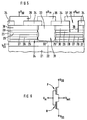
- FIG. 4 shows a plan view of the MOS transistor explained with reference to FIG. 3.
- the section shown in Figure 3 is designated in Figure 4 with III-III.
- the first opening 4 filled by the layer structure has a dimension of 1.2 ⁇ m ⁇ 2.2 ⁇ m in the example.
- the second opening determining the width of the transistor has a dimension of 0.8 ⁇ m x 0.8 ⁇ m.
- the contact holes on the third layer 7, which acts as a drain region, and the gate electrode 10 have a cross section of approximately 0.4 ⁇ m ⁇ 0.4 ⁇ m.
- the cross section of the second opening 8 is entered as a dashed line in FIG. 4.
- a main surface of a substrate 21 is made, for example, of p-doped single-crystal Silicon exists, a source connection region 22 is formed (see FIG. 4).
- the source connection region 22 is, for example, n+-doped with a dopant concentration of 1020 cm ⁇ 3.
- the source connection region 22 can be designed as a continuous layer or as a trough.
- the source connection region 22 is preferably produced by diffusion.
- an insulating layer 23 is applied over the entire surface, which consists for example of SiO2 and which has a thickness of, for example, 350 nm.
- a first opening 24 is opened in the insulating layer 23.
- the first opening 24 is produced with the aid of a lithography step, for example by anisotropic etching.
- the surface of the source connection region 22 is exposed within the first opening 24.
- a layer structure of silicon is grown within the first opening 24 by selective epitaxy, which layer essentially fills the first opening 24.
- the selective epitaxy in which silicon essentially only grows on the surface of silicon, while no silicon grows on the surface of the insulating layer 23, is used, for example, as RTP-CVD epitaxy with SiH2Cl2 gas in the temperature range from 400 to 700 ° C and carried out in the pressure range from 0.1 to 10 mbar.
- the layers are deposited in situ doped by adding an appropriate doping gas.
- a first layer 25, which forms a source region, is grown on the surface of the source connection region 22 and is n+-doped with a dopant concentration of approximately 1020 cm ⁇ 3.
- the first layer 25 is grown in a thickness of approximately 50 to 100 nm.
- the second layer 26 forms a channel region in the inverter.
- the second layer 26 has a dopant concentration of about 1018 cm ⁇ 3.
- a third layer 27 is grown, which is n+-doped with a dopant concentration of about 1020 cm ⁇ 3 and a thickness of about 50 to 100 nm.
- a fourth layer 28 is grown, which is p+-doped with a dopant concentration of about 1020 cm ⁇ 3 and which is grown in a thickness of about 50 to 100 nm.
- a fifth layer 29 is grown, which is n-doped with a dopant concentration of about 1018 cm ⁇ 3 and which is grown in a thickness of about 50 nm.
- the fifth layer 29 forms a channel region in the finished inverter.
- a sixth layer 30 is grown on the fifth layer 29, which is p+-doped with a dopant concentration of about 1020 cm ⁇ 3 and which is deposited in a thickness of about 50 to 100 nm.
- the sixth layer 30 is essentially level with the surface of the insulating layer 23.
- a second opening 8 is produced using a lithography step extends at least into the first layer 25.
- the second opening 31 preferably extends to the surface of the source connection region 22.
- An oxidation is then carried out at preferably 700 to 800 ° C., in which a gate dielectric 32 is formed along the surface of the second opening 31.
- the oxidation time will adjusted so that a layer thickness of approximately 5 nm is formed on the surface of the second layer 26 and the fifth layer 29, which each form channel regions in the inverter. Because of the difference in the dopant concentration, an approximately five times increased layer thickness is formed on the surface of the higher doped first layer 25, third layer 27, fourth layer 28, sixth layer 30 and the source connection region 22.
- an SiO 2 layer is formed on the surface of the sixth layer 30 outside the second opening 31, which is not shown in FIG. 5 for the sake of clarity.
- the remaining free space within the second opening 31 is filled with n+-doped polysilicon to form a gate electrode 33.
- an insulation layer 34 made of, for example, SiO2 is applied on the surface of the insulating layer 23, the sixth layer 30 and the gate electrode 33.
- a third opening is created by the insulation layer 34, the sixth layer 30 and the fifth layer 29, which extends to the surface of the fourth layer 28.
- the side walls of the third opening 35 are provided with insulating spacers 36.
- the insulating spacers 36 are produced, for example, by conformal deposition of a thin SiO2 layer and subsequent anisotropic etching of the SiO2 layer.
- the third opening 35 is filled with a metallization, an output contact 37 being formed.
- a contact hole on the gate electrode 33 is opened in the insulation layer 34 and provided with a metallization.
- a further contact hole is opened in the insulation layer 34, which extends onto the surface of the sixth layer 30 and which is provided with a metallization.
- the source connection region 22 is via a contact hole filled with a metallization in the insulation layer 34 and the insulating layer 23 outside the in Figure 5 shown section contacted and connected in operation to a second supply voltage V SS .
- the source connection region 22, the first layer 25, the second layer 26 and the third layer 27 together with the gate dielectric 32 and the gate electrode 33 form an n-channel MOS transistor N of the inverter (see FIG. 6).
- the second layer 26 acts as a channel region
- the source connection region 22 and the first layer 25 act as a source and the third layer 27 as a drain.
- the fourth layer 28, the fifth layer 29, the sixth layer 30, the gate dielectric 32 and the gate electrode 33 form a p-channel MOS transistor P of the inverter (see FIG. 6).
- the fifth layer 29 acts as a channel area
- the fourth layer 28 acts as a source connection area
- the sixth layer 30 acts as a drain area.
- the fourth layer 27 is connected to the fifth layer 28 via a tunnel effect or the contact 35, which occur at dopant concentrations of 1020 cm ⁇ 3 between an n+-doped region and a p+-doped region.
- the output contact 37 thus also makes contact with the third layer 27 via the fourth layer 28.
- an input signal V in is applied via the input contact 38 and an output signal V out is taken off via the output contact 37.
- a ring oscillator By arranging a plurality of inverters in adjacent first openings next to one another and connecting the output contact of one inverter to the input contact of the next inverter, a ring oscillator can be easily constructed using the manufacturing method according to the invention.
Landscapes
- Metal-Oxide And Bipolar Metal-Oxide Semiconductor Integrated Circuits (AREA)
- Insulated Gate Type Field-Effect Transistor (AREA)
- Thin Film Transistor (AREA)
Abstract
Description
- In integrierten Schaltungen werden CMOS-Transistoren und logische Gatter derzeit meist in einer planaren Siliziumtechnologie realisiert, bei der Source, Kanalbereich und Drain lateral angeordnet sind. Die erreichbaren Gatelängen sind dabei abhängig vom Auflösungsvermögen der verwendeten optischen Lithographie und von Toleranzen bei der Strukturierung und Justierung. In der 16 M-Generation werden typische Gatelängen von 0,6 µm, in der 64 M-Generation von 0,35 µm erreicht.
- Im Hinblick auf die elektrischen Eigenschaften von MOS-Transistoren sowie auf eine erhöhte Packungsdichte, die insbesondere bei komplexen logischen Schaltungen wie logischen Gattern bedeutsam wird, da dort mehrere n- und p-Kanaltransistoren zusätzlich gegeneinander isoliert und miteinander verdrahtet werden müssen, wird eine weitere Verkleinerung der lateralen Kanallängen angestrebt. Dazu sind Verbesserungen der optischen Lithographie sowie der Lack- und Ätztechnik erforderlich. Wegen des begrenzten Auflösungsvermögens der optischen Lithographie und zunehmender Probleme mit Toleranzen bei der Strukturierung und Justierung erscheint es jedoch fraglich, ob sich auf diese Weise reproduzierbar Transistoren mit Kanallängen unter 100 nm herstellen lassen. Darüber hinaus führt die Verkleinerung der lateralen Kanallänge zu Veränderungen der elektrischen Eigenschaften des MOS-Transistors, die durch eine Implantation von Dotierstoffen im Kanalgebiet sowie aufwendige Source/Drain-Konstruktionen ausgeglichen werden müssen.
- Geringere Strukturgrößen in planarer Technologie können erzielt werden, wenn die optische Lithographie durch Elektronenstrahllithographie ersetzt wird. Im Labormaßstab ist es bisher gelungen, mit einem Elektronenstrahlschreiber einzelne funktionsfähige MOSTransistoren mit Kanallängen bis zu 50 nm herzustellen. Da die Elektronenstrahllithographie jedoch langsam ist, erscheint sie für einen Einsatz in einer Halbleiterfertigung aus wirtschaftlichen Gründen als ungeeignet.
- In den achtziger Jahren ist vorgeschlagen worden (siehe zum Beispiel F. E. Holmes et al, Solid State Electronics, 17 (1974), S. 791 ff) in der sogenannten V-MOS-Technologie vertikale Transistoren herzustellen. Dabei werden Source, Kanalbereich und Drain als vertikale Schichtenfolgen in einem Substrat realisiert. Gatedielektrikum und Gateelektrode werden an der Oberfläche eines Grabens, der ein V-förmiges Profil aufweist, realisiert. Dadurch konnten Transistoren mit kürzeren Kanallängen hergestellt werden, als es die damalige Lithographie erlaubte. Da in diesen Transistoren jedoch nur die Kanallänge klein war, traten bei dieser Technik große parasitäre Kapazitäten auf. Daher hat dieser Vorschlag in der Logikentwicklung gegenüber planaren Herstellungsverfahren keine Bedeutung erlangt.
- In der DRAM-Speicherentwicklung wurde von Texas Instruments (siehe zum Beispiel W. F. Richardson et al, IEDM Dig. Tech. Paper (1985), S. 714 bis 717) vorgeschlagen, in der sogenannten "Trench Tranistor Zelle" Transistor und Kondensator vertikal zu integrieren. Der dort vorgeschlagene Transistor weist eine Kanallänge im Bereich von etwa 1 µm auf. In der Speicherentwicklung hat sich in der Folge nur die Anordnung des Kondensators im Trench durchgesetzt.
- In der Einleitung zur Dissertation von W. Kiunke, 1992, Seite 2 bis 3, wird ein Überblick über Einsatzmöglichkeiten der Molekularstrahlepitaxie gegeben. Bei der Molekularstrahlepitaxie können kontrolliert homogene Schichten mit einer minimalen Dicke um eine Atomlage hergestellt werden. Durch Zugabe von Dotierstoff enthaltendem Gas ist eine Dotierung im Bereich von 10¹⁴ cm⁻³ bis 10²⁰ cm⁻³ in situ während der Epitaxie möglich. Als Anwendungsbeispiel wird über einen Vorschlag für einen vertikalen CMOS-Inverter berichtet. Der vorgeschlagene Inverter ist als Mesastruktur auf einem Substrat realisiert. Die Mesastruktur umfaßt eine npnpnp-Schichtenfolge mit senkrechten Flanken. An einer Seite sind sämtliche senkrechten Flanken der Schichten mit einem Gatedielektrikum und einer Gateelektrode versehen. Die Gateelektrode ist gegenüber dem Substrat nur durch das Gatedielektrikum isoliert, so daß dieser Aufbau große parasitäre Kapazitäten aufweist.
- Der Erfindung liegt das Problem zugrunde, ein Herstellungsverfahren für MOS-Transistoren mit definierter Kanallänge im Bereich bis unter 50 nm anzugeben. Das Verfahren soll insbesondere geeignet sein zur Herstellung von kompakten, schnellen logischen Gattern.
- Dieses Problem wird erfindungsgemäß gelöst durch ein Verfahren nach Anspruch 1. Weitere Ausgestaltungen der Erfindung gehen aus den übrigen Ansprüchen hervor.
- In dem erfindungsgemäßen Verfahren wird an einer Hauptfläche eines Substrats ein Sourceanschlußgebiet erzeugt. Als Substrat wird insbesondere ein Siliziumwafer verwendet. Das Sourceanschlußgebiet kann an der Hauptfläche des Siliziumwafers sowohl als durchgehende entsprechend dotierte Schicht als auch als dotierte Wanne gebildet werden. Alternativ kann als Substrat auch ein SOI-Substrat verwendet werden. In diesem, das eine Siliziumscheibe, eine darauf angeordnete isolierende Schicht und eine darauf angeordnete einkristalline Siliziumschicht umfaßt, wird das Sourceanschlußgebiet in der einkristallinen Siliziumschicht realisiert. Zur Erzielung höchster Packungsdichte wird es von einem isolierenden Graben umgeben.
- Nach Erzeugung des Sourceanschlußgebietes wird auf die Hauptfläche ganzflächig eine isolierende Schicht aufgebracht, in der eine erste Öffnung erzeugt wird. Innerhalb der ersten Öffnung liegt die Oberfläche für das spätere Sourcegebiet frei. Durch epitaktisches Aufwachsen von dotiertem Halbleitermaterial wird in der ersten Öffnung eine vertikale Schichtenfolge erzeugt, die mindestens einen Kanalbereich und ein Draingebiet und vorzugsweise zusätzlich ein Sourcegebiet für den MOS-Transistor umfaßt. Umfaßt die Schichtenfolge nur den Kanalbereich und das Draingebiet, so wirkt das Sourceanschlußgebiet auch als Sourcegebiet.
- Zur Herstellung der vertikalen Schichtenfolge sind alle Epitaxieverfahren geeignet. Vorzugsweise wird die Schichtenfolge durch Molekularstrahlepitaxie , mit der besonders dünne Schichten hergestellt werden können, oder durch eine selektive Epitaxie, insbesondere in einem RTP-CVD-Verfahren mit SiH₂Cl₂-Gas, wobei jeweils zur insitu-Dotierung ein entsprechendes Dotiergas zugegeben wird, hergestellt. Wird zum Aufwachsen der Schichtenfolge ein nicht selektives Verfahren verwendet, so wächst Halbleitermaterial sowohl auf der Oberfläche des Sourceanschlußgebietes als auch auf der Oberfläche der isolierenden Schicht auf. Auf der Oberfläche des Sourceanschlußgebietes wächst das Halbleitermaterial einkristallin, auf der Oberfläche der isolierenden Schicht jedoch polykristallin auf. Das polykristalline Halbleitermaterial kann anschließend selektiv zum einkristallinen Schichtaufbau entfernt werden. Die Anwendung eines selektiven Epitaxieverfahrens hat den Vorteil, daß dieser Ätzschritt entfällt.
- In der Schichtenfolge wird anschließend eine zweite Öffnung erzeugt, die mindestens so tief ist, wie es der Summe der Dicken von Draingebiet und Kanalbereich und gegebenenfalls zusätzlich des Sourcegebietes entspricht. Auf der Oberfläche der zweiten Öffnung wird ein Gatedielektrikum und darauf eine Gateelektrode aufgewachsen. Im Betrieb des auf diese Weise hergestellten MOS-Transistors bildet sich entlang der Oberfläche der zweiten Öffnung im Kanalbereich ein leitender Kanal aus. Da die zweite Öffnung im Innern des Schichtaufbaus, wo das Kristallgefüge im wesentlichen defektfrei ist, angeordnet wird, lassen sich im erfindungsgemäßen Verfahren MOS-Transistoren mit guten elektrischen Eigenschaften herstellen.
- Das erfindungsgemäße Herstellverfahren ist geeignet zum Aufbau eines Inverters, der zwei zueinander komplementäre Transistoren umfaßt. Dazu werden Schichtenfolgen mit entsprechenden Dotierungen in der ersten Öffnung aufgewachsen.
- Schichten, die in der Schaltung Source/Drain-Gebiete bilden, werden hochdotiert und in einer Dicke von 50 bis 200 nm abgeschieden. Schichten, die in der Schaltung Kanalbereiche bilden, werden schwächer dotiert mit Dotierstoffkonzentrationen im Bereich 10¹⁷ bis 10¹⁸ cm⁻³ und werden in einer Dicke von 10 bis 200 nm, vorzugsweise 50 bis 100 nm abgeschieden. Die Dicke dieser Schichten entspricht der Kanallänge des entsprechenden MOS-Transistors.
- Es ist besonders vorteilhaft, die Schichtdicken auf die Tiefe der ersten Öffnung so abzustimmen, daß die Schichtenfolge mit der Oberfläche der isolierenden Schicht im wesentlichen planar abschließt. Dadurch wird eine Schaltunganordnung mit planarem Aufbau erzielt.
- Es ist besonders vorteilhaft, diejenigen Schichten, die Kanalbereiche bilden, mit einer Dotierung von kleiner oder gleich 10¹⁸ cm⁻³ zu versehen, wahrend diejenigen Schichten, die Source/Drain-Gebiete bilden, mit einer Dotierung von größer oder gleich 10¹⁹ cm³ versehen werden, und das Gatedielektrikum durch thermische Oxidation bei 700 bis 800°C zu bilden. Dabei bildet sich das Gatedielektrikum auf den höher dotierten Gebieten mit etwa fünffacher Dicke im Vergleich zu den schwächer dotierten Schichten, die als Kanalbereich eingesetzt werden. Die größere
- Dicke des Gatedielektrikums an der Oberfläche der Source/Drain-Gebiete bewirkt eine Reduktion der Überlappkapazitäten.
- Im folgenden wird die Erfindung anhand der Ausführungsbeispiele und der Figuren näher erläutert.
- Figur 1
- zeigt ein Substrat mit einem Sourceanschlußgebiet und einer isolierenden Schicht, die eine Öffnung aufweist.
- Figur 2
- zeigt das Substrat nach Erzeugung eines Schichtaufbaus in der Öffnung der isolierenden Schicht.
- Figur 3
- zeigt einen vertikalen MOS-Transistor, der in den Schichtaufbau realisiert ist.
- Figur 4
- zeigt einen Aufblick auf den vertikalen MOS-Transistor.
- Figur 5
- zeigt einen vertikalen Inverter, der in einem Schichtaufbau realisiert ist.
- Figur 6
- zeigt ein Prinzipschaltbild des Inverters.
- Zur Herstellung eines MOS-Transistors wird an einer Hauptfläche eines Substrats 1 aus zum Beispiel p-dotiertem, einkristallinem Silizium, ein Sourceanschlußgebiet 2 erzeugt. Das Sourceanschlußgebiet 2 wird n⁺-dotiert. Das Sourceanschlußgebiet 2 wird mit P, Sb oder As dotiert und weist eine Dotierstoffkonzentration von etwa 10²⁰ cm⁻³ auf. Das Sourceanschlußgebiet 2 kann als durchgehende Schicht oder als Wanne realisiert sein (siehe Figur 1).
- Es wird eine isolierende Schicht 3 aufgebracht, die die Oberfläche des Sourceanschlußgebietes 2 bedeckt. Die isolierende Schicht 3 wird zum Beispiel aus SiO₂ erzeugt. Dies erfolgt durch Abscheidung in einer Dicke von etwa 200 nm oder durch Oxidation in entsprechender Dicke.
- In der isolierenden Schicht 3 wird mit einem Lithographieschritt eine erste Öffnung 4 erzeugt. Die erste Öffnung 4 wird zum Beispiel durch anisotropes Ätzen gebildet. Im Bereich der ersten Öffnung 4 liegt die Oberfläche des Sourceanschlußgebietes 2 frei.
- Innerhalb der ersten Öffnung 4 wird vorzugsweise durch selektive Epitaxie ein Schichtaufbau aus Silizium erzeugt, der die erste Öffnung 4 im wesentlichen ausfüllt und mit der isolierenden Schicht 3 eine im wesentlichen ebene Oberfläche bildet. Als selektive Epitaxie ist insbesondere eine Molekularstrahlepitaxie im Temperaturbereich zwischen 400 und 700°c und im Druckbereich zwischen 0,1 mbar und 10 mbar oder ein RTP-CVD-Verfahren mit SiH₂Cl₂-Gas als Prozeßgas geeignet. Die Dotierung der die Schichtenfolge bildenden Schichten erfolgt insitu bei der Epitaxie durch Zugabe eines Dotierstoff enthaltenden Gases zum Prozeßgas. Zur Erzeugung von n-dotierten Schichten wird insbesondere AsH₃, SbH₃ oder PH₃ zugegeben. Zur Herstellung von p-dotierten Schichten wird insbesondere B₂H₆ zugegeben.
- In der ersten Öffnung 4 wird auf der Oberfläche des Sourceanschlußgebietes 2 eine erste Schicht 5 aufgewachsen. Die erste Schicht 5 wird durch Zugabe von Sb oder As mit einer Dotierstoffkonzentration von etwa 10²⁰ cm⁻³ n⁺-dotiert. Die erste Schicht 5 wird in einer Schichtdicke von etwa 50 nm aufgewachsen (siehe Figur 2).
- Auf die erste Schicht 5 wird eine zweite Schicht 6 aufgewachsen, die durch Zugabe von B₂H₆ bei der Epitaxie insitu-p-dotiert wird. Die zweite Schicht 5 weist eine Dotierstoffkonzentration von etwa 10¹⁸cm⁻³ und eine Dicke von etwa 50 nm auf. Die zweite Schicht 5 bildet ein Kanalgebiet.
- Auf die zweite Schicht 6 wird eine dritte Schicht 7 aufgewachsen,die ein Draingebiet bildet. Die dritte Schicht 7 wird n⁺-dotiert mit einer Dotierstoffkonzentration von etwa 10²⁰ cm⁻³. Dazu wird bei der selektiven Epitaxie dem Prozeßgas AsH₃ zugegeben. Die dritte Schicht 7 wird in einer Schichtdicke von etwa 100 nm aufgewachsen. Die erste Schicht 5, die zweite Schicht 6 und die dritte Schicht 7 bilden einen Schichtaufbau, der die erste Öffnung 4 vollständig ausfüllt (siehe Figur 2).
- In dem aus erster Schicht 5, zweiter Schicht 6 und dritter Schicht 7 gebildeten Schichtaufbau wird unter Verwendung eines Lithographieschrittes eine zweite Öffnung 8 geätzt. Die zweite Öffnung 8 muß mindestens bis in die erste Schicht 5 hineinreichen. Vorzugsweise wird die zweite Öffnung 8 bis auf die Oberfläche des Sourceanschlußgebietes 2 geätzt (siehe Figur 3).
- Anschließend wird durch Oxidation bei einer Temperatur im Bereich zwischen 700 und 800°C ein Gatedielektrikum 9 erzeugt. Die Oxidationszeit wird dabei so eingestellt, daß sich an der Oberfläche der zweiten Schicht 6 eine Dicke des Gatedielektrikums 9 von etwa 5 nm einstellt. In dieser Zeit bildet sich an der Oberfläche der hochdotierten ersten Schicht 5, dritten Schicht 7 sowie des Sourceanschlußgebietes eine um den Faktor 5 größere Dicke. Dieses bewirkt eine Reduktion der Überlappkapazität.
- Anschließend wird der verbleibende Freiraum innerhalb der zweiten Öffnung 8 mit n⁺-dotiertem Polysilizium aufgefüllt. Das n⁺-dotierte Polysilizium bildet eine Gateelektrode 10.
- Die dritte Schicht 7, die n⁺-dotiert ist, bildet ein Draingebiet, die zweite Schicht 6, die p-dotiert ist, bildet ein Kanalgebiet, die erste Schicht 5, die ein Sourcegebiet bildet, und das Sourceanschlußgebiet 2, die jeweils n⁺-dotiert sind, bilden gemeinsam das wirksame Sourcegebiet des MOS-Transistors. Die erste Schicht 5 wird auf das Sourceanschlußgebiet 2 aufgewachsen, um eine lineare, vertikale Anordnung von Source, Kanal und Drain sicherzustellen. Die Weite des MOS-Transistors ist bestimmt durch den Umfang der zweiten Öffnung 8. Die Kanallänge des MOS-Transistors ist bestimmt durch die Dicke der zweiten Schicht 6. Mit Hilfe von Molekularstrahlepitaxie oder eines RTP-CVD-Verfahrens, das im Temperaturbereich 400°C und 700°C und Druckbereich zwischen 0,1 mbar und 10 mbar eingesetzt wird, können Schichten mit minimalen Dicken bis zu 5 nm hergestellt werden. Diese Schichtdicke ist die Untergrenze der Kanallänge, die mit dem erfindungsgemäßen Herstellverfahren hergestellt werden kann.
- Auf die isolierende Schicht 3, die dritte Schicht 7, und die die Gateelektrode 10 bildende Polysiliziumfüllung wird ganzflächig eine Isolationsschicht 11 aufgebracht. In der Isolationsschicht 11 werden Kontaktlocher zur Gateelektrode 10 sowie zur dritten Schicht 7, die als Draingebiet wirkt, geöffnet und mit Metallisierungen 12 versehen. Seitlich der ersten Öffnung 4 wird das Sourceanschlußgebiet 2 zum Beispiel durch ein tiefreichendes mit einer Metallisierung gefülltes Kontaktloch, das die Isolationsschicht 11 und die isolierende Schicht 3 durchquert, kontaktiert. Im Betrieb des MOS-Transistors wird das Sourceanschlußgebiet 2 mit der Versorgungsspannung VSS, die dritte Schicht 7 mit der Versorgungsspannung VDD und die Gateelektrode 10 mit der Gatespannung G verbunden.
- Figur 4 zeigt eine Aufsicht auf den anhand von Figur 3 erläuterten MOS-Transistor. Der in Figur 3 dargestellte Schnitt ist in Figur 4 mit III-III bezeichnet. Die vom Schichtaufbau ausgefüllte erste Öffnung 4 weist im Beispiel einer Abmessung von 1,2 µm x 2,2 µm auf. Die die Weite des Transistors bestimmende zweite Öffnung hat eine Abmessung von 0,8 µm x 0,8 µm. Die Kontaktlöcher auf die dritte Schicht 7, die als Draingebiet wirkt sowie die Gateelektrode 10 weisen einen Querschnitt von etwa 0,4 µm x 0,4 µm auf. Der Querschnitt der zweiten Öffnung 8 ist als gestrichelte Linie in Figur 4 eingetragen.
Zur Herstellung eines Inverters wird bei einer Hauptfläche eines Substrats 21, das zum Beispiel aus p-dotiertem einkristallinem Silizium besteht, ein Sourceanschlußgebiet 22 gebildet (siehe Figur 4). Das Sourceanschlußgebiet 22 ist zum Beispiel n⁺-dotiert mit einer Dotierstoffkonzentration von 10²⁰ cm⁻³. Das Sourceanschlußgebiet 22 kann als durchgehende Schicht oder als Wanne ausgebildet sein. Das Sourceanschlußgebiet 22 wird vorzugsweise durch Diffusion hergestellt. - Auf das Sourceanschlußgebiet 22 wird ganzflächig eine isolierende Schicht 23 aufgebracht, die zum Beispiel aus SiO₂ besteht und die eine Dicke von zum Beispiel 350 nm aufweist. In der isolierenden Schicht 23 wird eine erste Öffnung 24 geöffnet. Die erste Öffnung 24 wird mit Hilfe eines Lithographieschrittes zum Beispiel durch anisotropes Ätzen erzeugt. Innerhalb der ersten Öffnung 24 wird die Oberfläche des Sourceanschlußgebietes 22 freigelegt.
- Innerhalb der ersten Öffnung 24 wird durch selektive Epitaxie ein Schichtaufbau aus Silizium aufgewachsen, der die erste Öffnung 24 im wesentlichen auffüllt. Die selektive Epitaxie, bei der Silizium im wesentlichen nur auf der Oberfläche von Silizium aufwächst, während auf der Oberfläche der isolierenden Schicht 23 kein Silizium aufwächst, wird zum Beispiel als RTP-CVD-Epitaxie mit SiH₂Cl₂-Gas im Temperaturbereich von 400 bis 700°C und im Druckbereich von 0,1 bis 10 mbar durchgeführt. Durch Zugabe eines entsprechenden Dotiergases werden die Schichten insitu dotiert abgeschieden.
- In der ersten Öffnung 24 wird auf der Oberfläche des Sourceanschlußgebietes 22 eine erste Schicht 25, die ein Sourcegebiet bildet, aufgewachsen, die n⁺-dotiert mit einer Dotierstoffkonzentration von etwa 10²⁰ cm⁻³ ist. Die erste Schicht 25 wird in - einer Dicke von etwa 50 bis 100 nm aufgewachsen.
- Auf die erste Schicht 25 wird eine zweite Schicht 26 aufgewachsen, die p-dotiert ist und die eine Dicke von etwa 50 nm aufweist. Die zweite Schicht 26 bildet im Inverter ein Kanalgebiet. Die zweite Schicht 26 weist eine Dotierstoffkonzentration von etwa 10¹⁸ cm⁻³ auf.
- Auf die zweite Schicht 26 wird eine dritte Schicht 27 aufgewachsen, die n⁺-dotiert ist mit einer Dotierstoffkonzentration von etwa 10²⁰ cm⁻³ und eine Dicke von etwa 50 bis 100 nm aufweist.
- Auf die dritte Schicht 27 wird eine vierte Schicht 28 aufgewachsen, die p⁺-dotiert wird mit einer Dotierstoffkonzentration von etwa 10²⁰ cm⁻³ und die in einer Dicke von etwa 50 bis 100 nm aufgewachsen wird.
- Auf die vierte Schicht 28 wird eine fünfte Schicht 29 aufgewachsen, die n-dotiert wird mit einer Dotierstoffkonzentration von etwa 10¹⁸ cm⁻³ und die in einer Dicke von etwa 50 nm aufgewachsen wird. Die fünfte Schicht 29 bildet im fertigen Inverter ein Kanalgebiet.
- Auf die fünfte Schicht 29 wird eine sechste Schicht 30 aufgewachsen, die p⁺-dotiert wird mit einer Dotierstoffkonzentration von etwa 10²⁰ cm⁻³ und die in einer Dicke von etwa 50 bis 100 nm abgeschieden wird. Die sechste Schicht 30 schließt in der Höhe im wesentlichen mit der Oberfläche der isolierenden Schicht 23 ab.
- In dem Schichtaufbau, der aus der ersten Schicht 25, der zweiten Schicht 26, der dritten Schicht 27, der vierten Schicht 28, der fünften Schicht 29 und der sechsten Schicht 30 gebildet wird, wird unter Verwendung eines Lithographieschrittes eine zweite Öffnung 8 erzeugt, die mindestens bis in die erste Schicht 25 hineinreicht. Vorzugsweise reicht die zweite Öffnung 31 bis auf die Oberfläche des Sourceanschlußgebietes 22.
- Nachfolgend wird bei vorzugsweise 700 bis 800°C eine Oxidation durchgeführt, bei der entlang der Oberfläche der zweiten Öffnung 31 ein Gatedielektrikum 32 gebildet wird. Die Oxidationszeit wird so eingestellt, daß an der Oberfläche der zweiten Schicht 26 sowie der fünften Schicht 29, die im Inverter jeweils Kanalgebiete bilden, eine Schichtdicke von etwa 5 nm entsteht. Wegen des Unterschiedes in der Dotierstoffkonzentration entsteht dabei an der Oberfläche der höher dotierten ersten Schicht 25, dritten Schicht 27, vierten Schicht 28, sechsten Schicht 30 und des Sourceanschlußgebietes 22 eine etwa fünffach vergrößerte Schichtdicke. Gleichzeitig entsteht an der Oberfläche der sechsten Schicht 30 außerhalb der zweiten Öffnung 31 eine SiO₂-Schicht, die der Übersichtlichkeit halber in Figur 5 nicht dargestellt ist.
- Der verbliebene Freiraum innerhalb der zweiten Öffnung 31 wird zur Bildung einer Gateelektrode 33 mit n⁺-dotiertem Polysilizium aufgefüllt.
- Auf die Oberfläche der isolierenden Schicht 23, der sechsten Schicht 30 und der Gateelektrode 33 wird eine Isolationsschicht 34 aus zum Beispiel SiO₂ aufgebracht. Es wird durch die Isolationsschicht 34, die sechste Schicht 30 und die fünfte Schicht 29 eine dritte Öffnung erzeugt, die bis auf die Oberfläche der vierten Schicht 28 reicht. Die Seitenwände der dritten Öffnung 35 werden mit isolierenden Spacern 36 versehen. Die isolierenden Spacer 36 werden zum Beispiel durch konforme Abscheidung einer dünnen SiO₂-Schicht und anschließendes anisotropes Ätzen der SiO₂-Schicht hergestellt. Die dritte Öffnung 35 wird mit einer Metallisierung aufgefüllt, wobei ein Ausgangskontakt 37 gebildet wird. Zur Bildung eines Eingangskontaktes 36 wird in die Isolationsschicht 34 ein Kontaktloch auf die Gateelektrode 33 geöffnet und mit einer Metallisierung versehen. Zur Herstellung eines Kontaktes 39 für eine erste Versorgungsspannung VDD wird in der Isolationsschicht 34 ein weiteres Kontaktloch geöffnet, das auf die Oberfläche der sechsten Schicht 30 reicht und das mit einer Metallisierung versehen wird. Das Sourceanschlußgebiet 22 wird über ein mit einer Metallisierung gefüllten Kontaktloch in der Isolationsschicht 34 und der isolierenden Schicht 23 außerhalb des in Figur 5 gezeigten Ausschnittes kontaktiert und im Betrieb mit einer zweiten Versorgungsspannung VSS verbunden.
- Das Sourceanschlußgebiet 22, die erste Schicht 25, die zweite Schicht 26 sowie die dritte Schicht 27 bilden mit dem Gatedielektrikum 32 und der Gateelektrode 33 einen n-Kanal-MOS-Transistor N des Inverters (siehe Figur 6). In dem n-Kanal-Transistor N wirkt die zweite Schicht 26 als Kanalgebiet, während Sourceanschlußgebiet 22 und erste Schicht 25 als Source wirken und die dritte Schicht 27 als Drain. Die vierte Schicht 28, die fünfte Schicht 29, die sechste Schicht 30, das Gatedielektrikum 32 und die Gateelektrode 33 bilden einen p-Kanal-MOS-Transistor P des Inverters (siehe Figur 6). Dabei wirkt die fünfte Schicht 29 als Kanalgebiet, wahrend die vierte Schicht 28 als Sourceanschlußgebiet und die sechste Schicht 30 als Draingebiet wirken. Die vierte Schicht 27 ist mit der fünften Schicht 28 über einen Tunneleffekt beziehungsweise den Kontakt 35 verbunden, der bei Dotierstoffkonzentrationen von 10²⁰ cm⁻³ zwischen einem n⁺-dotierten Gebiet und einem p⁺-dotierten Gebiet auftreten. Der Ausgangskontakt 37 kontaktiert damit über die vierte Schicht 28 auch die dritte Schicht 27. In dem Inverter wird ein Eingangssignal Vin über den Eingangskontakt 38 angelegt und ein Ausgangssignal Vout über den Ausgangskontakt 37 abgenommen.
- Durch Anordnen mehrerer Inverter in benachbarten ersten Öffnungen nebeneinander und Verbinden jeweils des Ausgangskontaktes des einen Inverters mit dem Eingangskontakt des nächsten Inverters kann unter Verwendung des erfindungsgemaßen Herstellverfahrens auf einfache Weise ein Ringoszillator aufgebaut werden.
Claims (10)
- Verfahren zur Herstellung einer integrierten Schaltungsanordnung mit mindestens einem MOS-Transistor,- bei dem an einer Hauptfläche eines Substrats (1) ein Sourceanschlußgebiet (2) erzeugt wird, das von einem ersten Leitfähigkeitstyp dotiert ist,- bei dem ganzflächig eine isolierende Schicht (3) aufgebracht wird,- bei dem in der isolierenden Schicht (3) eine erste Öffnung (4) erzeugt wird, die auf die Oberfläche des Sourceanschlußgebietes (2) reicht und in der die Oberfläche des Sourceanschlußgebietes (2) teilweise freigelegt wird,- bei dem in der ersten Öffnung durch epitaktisches Aufwachsen von Halbleitermaterial mit insitu-Dotierung eine vertikale Schichtenfolge (5, 6, 7) erzeugt wird, die mindestens einen Kanalbereich (6) und ein Draingebiet (7) für den MOS-Transistor umfaßt,- bei dem in der Schichtenfolge eine zweite Öffnung (8) erzeugt wird, die mindestens so tief ist, wie es der Summe der Dicken von Draingebiet (7) und Kanalbereich (6) entspricht,- bei dem auf die Oberfläche der zweiten Öffnung (8) ein Gatedielektrikum (9) aufgebracht wird,- bei dem auf das Gatedielektrikum (9) eine Gateelektrode (10) aufgebracht wird.
- Verfahren nach Anspruch 1,- bei dem der Schichtaufbau die erste Öffnung (4) so auffüllt, daß die Oberfläche des Schichtaufbaus (7) mit der Oberfläche der isolierenden Schicht (3) im wesentlichen eben abschließt,- bei dem die zweite Öffnung (8) mit leitfähigem Material im wesentlichen aufgefüllt wird, wobei das leitfähige Material die Gateelektrode (10) bildet.
- Verfahren nach Anspruch 1 oder 2,
bei dem die Schichtenfolge (5, 6, 7) durch Molekularstrahlepitaxie im Temperaturbereich zwischen 400 und 700°C und im Druckbereich zwischen 0,1 mbar und 10 mbar oder durch RTP-CVD-(Rapid thermal processing - chemical vapour deposition) mit SiH₂Cl₂-Gas oder SiH₄ aufgewachsen wird. - Verfahren nach einem der Ansprüche 1 bis 3,- bei dem in der ersten Öffnung (4) eine erste Schicht (5) aufgewachsen wird, die vom ersten Leitfähigkeitstyp dotiert ist,- bei dem auf die erste Schicht (5) eine zweite Schicht (6) aufgewachsen wird, die von einem zweiten, zum ersten entgegengesetzten Leitfähigkeitstyp dotiert ist und die einen Kanalbereich bildet,- bei dem auf die zweite Schicht (6) eine dritte Schicht aufgewachsen wird, die vom ersten Leitfähigkeitstyp dotiert ist.
- Verfahren nach Anspruch 4,
bei dem die erste Schicht (5) in einer Dicke von 50 bis 200 nm, die zweite Schicht (6) in einer Dicke von 10 bis 200 nm und die dritte Schicht in einer Dicke von 50 bis 200 nm aufgewachsen wird. - Verfahren nach einem der Ansprüche 1 bis 3,- bei dem in der ersten Öffnung (24) eine erste Schicht (25) aufgewachsen wird, die vom ersten Leitfähigkeitstyp dotiert ist,- bei dem auf die erste Schicht (25) eine zweite Schicht (26) aufgewachsen wird, die von einem zweiten, zum ersten entgegengesetzten Leitfähigkeitstyp dotiert ist und die einen Kanalbereich bildet,- bei dem auf die zweite Schicht (26) eine dritte Schicht (27) aufgewachsen wird, die vom ersten Leitfähigkeitstyp dotiert ist,- bei dem auf die dritte Schicht (27) eine vierte Schicht (28) aufgewachsen wird, die vom zweiten Leitfähigkeitstyp dotiert ist,- bei dem auf die vierte Schicht (28) eine fünfte Schicht (29) aufgewachsen wird, die vom ersten Leitfähigkeitstyp dotiert ist und die einen Kanalbereich bildet,- bei dem auf die fünfte Schicht (29) eine sechste Schicht (30) aufgewachsen wird, die vom zweiten Leitfähigkeitstyp dotiert ist,- bei dem eine dritte Öffnung (35) erzeugt wird, die bis auf die vierte Schicht (28) reicht, deren Seitenwände mit isolierenden Spacern (36) versehen werden und die mit leitfähigem Material aufgefüllt wird.
- Verfahren nach Anspruch 6,- bei dem die erste Schicht (25), die dritte Schicht (27), die vierte Schicht (28) und die sechste Schicht (30) jeweils in einer Dicke zwischen 50 nm und 200 nm aufgewachsen werden,- bei dem die zweite Schicht (26) und die fünfte Schicht (29) jeweils in einer Dicke zwischen 10 nm und 200 nm aufgewachsen werden.
- Verfahren nach einem der Ansprüche 1 bis 7,- bei dem in Schichten der Schichtenfolge, die keinen Kanalbereich bilden, eine Dotierstoffkonzentration von mindestens 10¹⁹ cm⁻³ eingestellt wird und in Schichten, die einen Kanalbereich bilden, eine Dotierstoffkonzentration zwischen 10¹⁷ cm⁻³ und 10¹⁸ cm⁻³ eingestellt wird,- bei dem durch thermische Oxidation bei 700 bis 800°C das Gatedielektrikum gebildet wird.
- Verfahren nach einem der Ansprüche 1 bis 8,- bei dem das Substrat (1) mindestens im Bereich der Hauptfläche einkristallines Silizium umfaßt, das von dem zweiten Leitfähigkeitstyp dotiert ist,- bei dem das Sourceanschlußgebiet (2) durch Implantation oder Diffusion mit von dem ersten Leitfähigkeitstyp dotierenden Ionen in der Hauptfläche des Substrats (1) erzeugt wird.
- Verfahren nach einem der Ansprüche 1 bis 8,- bei dem das Substrat (1) ein SOI-Substrat mit einer Siliziumscheibe, einer darauf angeordneten isolierenden Schicht und einer darauf angeordneten einkristallinen Siliziumschicht,- bei dem das Sourceanschlußgebiet (2) in der einkristallinen Schicht gebildet wird,- bei dem in der einkristallinen Schicht ein das Sourceanschlußgebiet (2) umgebender, isolierender Graben erzeugt wird.
Applications Claiming Priority (2)
| Application Number | Priority Date | Filing Date | Title |
|---|---|---|---|
| DE4340967 | 1993-12-01 | ||
| DE4340967A DE4340967C1 (de) | 1993-12-01 | 1993-12-01 | Verfahren zur Herstellung einer integrierten Schaltungsanordnung mit mindestens einem MOS-Transistor |
Publications (2)
| Publication Number | Publication Date |
|---|---|
| EP0656647A1 true EP0656647A1 (de) | 1995-06-07 |
| EP0656647B1 EP0656647B1 (de) | 1999-01-20 |
Family
ID=6503928
Family Applications (1)
| Application Number | Title | Priority Date | Filing Date |
|---|---|---|---|
| EP94117699A Expired - Lifetime EP0656647B1 (de) | 1993-12-01 | 1994-11-09 | Verfahren zur Herstellung einer integrierten Schaltungsanordnung mit mindestens einem MOS-Transistor |
Country Status (6)
| Country | Link |
|---|---|
| US (1) | US5443992A (de) |
| EP (1) | EP0656647B1 (de) |
| JP (1) | JP3851360B2 (de) |
| KR (1) | KR950021772A (de) |
| DE (2) | DE4340967C1 (de) |
| TW (1) | TW274635B (de) |
Families Citing this family (32)
| Publication number | Priority date | Publication date | Assignee | Title |
|---|---|---|---|---|
| EP0683921B1 (de) * | 1993-02-04 | 2004-06-16 | Cornell Research Foundation, Inc. | Mikrostrukturen und einzelmask, einkristall-herstellungsverfahren |
| DE4417150C2 (de) * | 1994-05-17 | 1996-03-14 | Siemens Ag | Verfahren zur Herstellung einer Anordnung mit selbstverstärkenden dynamischen MOS-Transistorspeicherzellen |
| US5872374A (en) * | 1996-03-29 | 1999-02-16 | Motorola, Inc. | Vertical semiconductor device |
| US5929476A (en) | 1996-06-21 | 1999-07-27 | Prall; Kirk | Semiconductor-on-insulator transistor and memory circuitry employing semiconductor-on-insulator transistors |
| DE19653107C2 (de) * | 1996-12-19 | 1998-10-08 | Siemens Ag | Verfahren zur Herstellung einer Speicherzellenanordnung |
| DE19711482C2 (de) * | 1997-03-19 | 1999-01-07 | Siemens Ag | Verfahren zur Herstellung eines vertikalen MOS-Transistors |
| US5864158A (en) * | 1997-04-04 | 1999-01-26 | Advanced Micro Devices, Inc. | Trench-gated vertical CMOS device |
| US6150687A (en) | 1997-07-08 | 2000-11-21 | Micron Technology, Inc. | Memory cell having a vertical transistor with buried source/drain and dual gates |
| US6072209A (en) | 1997-07-08 | 2000-06-06 | Micro Technology, Inc. | Four F2 folded bit line DRAM cell structure having buried bit and word lines |
| US6191470B1 (en) | 1997-07-08 | 2001-02-20 | Micron Technology, Inc. | Semiconductor-on-insulator memory cell with buried word and body lines |
| US6066869A (en) | 1997-10-06 | 2000-05-23 | Micron Technology, Inc. | Circuit and method for a folded bit line memory cell with vertical transistor and trench capacitor |
| US6528837B2 (en) * | 1997-10-06 | 2003-03-04 | Micron Technology, Inc. | Circuit and method for an open bit line memory cell with a vertical transistor and trench plate trench capacitor |
| US5907170A (en) | 1997-10-06 | 1999-05-25 | Micron Technology, Inc. | Circuit and method for an open bit line memory cell with a vertical transistor and trench plate trench capacitor |
| US6069390A (en) | 1998-01-15 | 2000-05-30 | International Business Machines Corporation | Semiconductor integrated circuits with mesas |
| US6177299B1 (en) | 1998-01-15 | 2001-01-23 | International Business Machines Corporation | Transistor having substantially isolated body and method of making the same |
| US6025225A (en) | 1998-01-22 | 2000-02-15 | Micron Technology, Inc. | Circuits with a trench capacitor having micro-roughened semiconductor surfaces and methods for forming the same |
| US6242775B1 (en) * | 1998-02-24 | 2001-06-05 | Micron Technology, Inc. | Circuits and methods using vertical complementary transistors |
| US6304483B1 (en) | 1998-02-24 | 2001-10-16 | Micron Technology, Inc. | Circuits and methods for a static random access memory using vertical transistors |
| US6097242A (en) | 1998-02-26 | 2000-08-01 | Micron Technology, Inc. | Threshold voltage compensation circuits for low voltage and low power CMOS integrated circuits |
| US6124729A (en) | 1998-02-27 | 2000-09-26 | Micron Technology, Inc. | Field programmable logic arrays with vertical transistors |
| US5991225A (en) | 1998-02-27 | 1999-11-23 | Micron Technology, Inc. | Programmable memory address decode array with vertical transistors |
| US6492232B1 (en) | 1998-06-15 | 2002-12-10 | Motorola, Inc. | Method of manufacturing vertical semiconductor device |
| US6134175A (en) | 1998-08-04 | 2000-10-17 | Micron Technology, Inc. | Memory address decode array with vertical transistors |
| US6208164B1 (en) | 1998-08-04 | 2001-03-27 | Micron Technology, Inc. | Programmable logic array with vertical transistors |
| US6500744B2 (en) | 1999-09-02 | 2002-12-31 | Micron Technology, Inc. | Methods of forming DRAM assemblies, transistor devices, and openings in substrates |
| KR100422412B1 (ko) * | 2001-12-20 | 2004-03-11 | 동부전자 주식회사 | 수직 실리콘-온-인슐레이터 구조의 원통형 트랜지스터 및그 제조 방법 |
| US7071519B2 (en) * | 2003-01-08 | 2006-07-04 | Texas Instruments Incorporated | Control of high-k gate dielectric film composition profile for property optimization |
| US6913959B2 (en) * | 2003-06-23 | 2005-07-05 | Advanced Micro Devices, Inc. | Method of manufacturing a semiconductor device having a MESA structure |
| US8618600B2 (en) * | 2008-06-09 | 2013-12-31 | Qimonda Ag | Integrated circuit including a buried wiring line |
| CN109326595B (zh) | 2017-07-31 | 2021-03-09 | 联华电子股份有限公司 | 半导体元件及其制作方法 |
| WO2023173679A1 (zh) * | 2022-03-18 | 2023-09-21 | 北京超弦存储器研究院 | 晶体管及其制作方法、存储器、电子设备 |
| CN116230763B (zh) * | 2022-03-18 | 2024-03-15 | 北京超弦存储器研究院 | Mos管、存储器及其制作方法 |
Citations (4)
| Publication number | Priority date | Publication date | Assignee | Title |
|---|---|---|---|---|
| US4740826A (en) * | 1985-09-25 | 1988-04-26 | Texas Instruments Incorporated | Vertical inverter |
| JPH0266969A (ja) * | 1988-08-31 | 1990-03-07 | Nec Corp | 半導体集積回路装置 |
| US4951102A (en) * | 1988-08-24 | 1990-08-21 | Harris Corporation | Trench gate VCMOS |
| US5072276A (en) * | 1986-10-08 | 1991-12-10 | Texas Instruments Incorporated | Elevated CMOS |
Family Cites Families (10)
| Publication number | Priority date | Publication date | Assignee | Title |
|---|---|---|---|---|
| US4412868A (en) * | 1981-12-23 | 1983-11-01 | General Electric Company | Method of making integrated circuits utilizing ion implantation and selective epitaxial growth |
| EP0098111B1 (de) * | 1982-06-24 | 1989-08-09 | Harris Semiconductor Patents, Inc. | Vertikaler Feldeffekttransistor mit isoliertem Gate und Verfahren zu desser Herstellung |
| US4788158A (en) * | 1985-09-25 | 1988-11-29 | Texas Instruments Incorporated | Method of making vertical inverter |
| US4824797A (en) * | 1985-10-31 | 1989-04-25 | International Business Machines Corporation | Self-aligned channel stop |
| US5164325A (en) * | 1987-10-08 | 1992-11-17 | Siliconix Incorporated | Method of making a vertical current flow field effect transistor |
| US4992838A (en) * | 1988-02-29 | 1991-02-12 | Texas Instruments Incorporated | Vertical MOS transistor with threshold voltage adjustment |
| US4942445A (en) * | 1988-07-05 | 1990-07-17 | General Electric Company | Lateral depletion mode tyristor |
| US4994871A (en) * | 1988-12-02 | 1991-02-19 | General Electric Company | Insulated gate bipolar transistor with improved latch-up current level and safe operating area |
| MY107475A (en) * | 1990-05-31 | 1995-12-30 | Canon Kk | Semiconductor device and method for producing the same. |
| US5240865A (en) * | 1990-07-30 | 1993-08-31 | Texas Instruments Incorporated | Method of forming a thyristor on an SOI substrate |
-
1993
- 1993-12-01 DE DE4340967A patent/DE4340967C1/de not_active Expired - Fee Related
-
1994
- 1994-10-15 TW TW083109590A patent/TW274635B/zh not_active IP Right Cessation
- 1994-11-01 US US08/332,733 patent/US5443992A/en not_active Expired - Lifetime
- 1994-11-09 DE DE59407691T patent/DE59407691D1/de not_active Expired - Lifetime
- 1994-11-09 EP EP94117699A patent/EP0656647B1/de not_active Expired - Lifetime
- 1994-11-30 JP JP32172394A patent/JP3851360B2/ja not_active Expired - Lifetime
- 1994-12-01 KR KR1019940032395A patent/KR950021772A/ko not_active Ceased
Patent Citations (4)
| Publication number | Priority date | Publication date | Assignee | Title |
|---|---|---|---|---|
| US4740826A (en) * | 1985-09-25 | 1988-04-26 | Texas Instruments Incorporated | Vertical inverter |
| US5072276A (en) * | 1986-10-08 | 1991-12-10 | Texas Instruments Incorporated | Elevated CMOS |
| US4951102A (en) * | 1988-08-24 | 1990-08-21 | Harris Corporation | Trench gate VCMOS |
| JPH0266969A (ja) * | 1988-08-31 | 1990-03-07 | Nec Corp | 半導体集積回路装置 |
Non-Patent Citations (2)
| Title |
|---|
| H. GOSSNER ET AL.: "Vertical Si-MOSFETs with Channel Lengths Down to 45 nm.", EXTENDED ABSTRACTS OF THE 1993 INT. CONF. ON SOLID STATE DEVICES AND MATERIALS, 29 August 1993 (1993-08-29), CIBA, JAPAN, pages 422 - 424, XP000409413 * |
| PATENT ABSTRACTS OF JAPAN vol. 14, no. 244 (E - 0932) 24 May 1990 (1990-05-24) * |
Also Published As
| Publication number | Publication date |
|---|---|
| KR950021772A (ko) | 1995-07-26 |
| EP0656647B1 (de) | 1999-01-20 |
| DE59407691D1 (de) | 1999-03-04 |
| JP3851360B2 (ja) | 2006-11-29 |
| JPH07202216A (ja) | 1995-08-04 |
| US5443992A (en) | 1995-08-22 |
| DE4340967C1 (de) | 1994-10-27 |
| TW274635B (de) | 1996-04-21 |
Similar Documents
| Publication | Publication Date | Title |
|---|---|---|
| EP0656647B1 (de) | Verfahren zur Herstellung einer integrierten Schaltungsanordnung mit mindestens einem MOS-Transistor | |
| EP0809279B1 (de) | Verfahren zur Herstellung eines MOS-Transistors | |
| DE3880750T2 (de) | Vertikale Transistor-/Kapazitätspeicherzellen-Struktur und Herstellungsverfahren dafür. | |
| DE19911149C1 (de) | Integrierte Schaltungsanordnung, die eine in einem Substrat vergrabene leitende Struktur umfaßt, die mit einem Gebiet des Substrats elektrisch verbunden ist, und Verfahren zu deren Herstellung | |
| DE4437068A1 (de) | Dünnfilmtransistor und Verfahren zu seiner Herstellung | |
| DE19632834C2 (de) | Verfahren zur Herstellung feiner Strukturen und dessen Verwendung zur Herstellung einer Maske und eines MOS-Transistors | |
| DE19525069C1 (de) | Verfahren zur Herstellung einer integrierten CMOS-Schaltung | |
| DE4428195C1 (de) | Verfahren zur Herstellung eines Siliziumkondensators | |
| EP1138085A2 (de) | Feldeffektgesteuerter transistor und verfahren zu dessen herstellung | |
| DE4341667C1 (de) | Integrierte Schaltungsanordnung mit mindestens einem CMOS-NAND-Gatter und Verfahren zu deren Herstellung | |
| DE19821777C1 (de) | Herstellverfahren für einen Kondensator in einer integrierten Speicherschaltung | |
| EP0864172B1 (de) | Verfahren zur herstellung einer integrierten schaltungsanordnung mit mindestens einem mos-transistor | |
| EP1155446B1 (de) | Verfahren zum herstellen einer dram-zelle mit einem grabenkondensator | |
| EP0875931B1 (de) | Verfahren zur Herstellung einer CMOS-Schaltungsanordnung | |
| EP0000180A1 (de) | Halbleiter-Zellenstruktur für eine Eimerkettenschaltung sowie Verfahren zur Herstellung derselben | |
| EP0520214B1 (de) | Verfahren zur Herstellung eines dotierten Gebietes in einem Substrat und Anwendung bei der Herstellung eines Bipolartransistors | |
| EP0510349B1 (de) | Verfahren zur Herstellung eines MOS-Transistors | |
| DE19923262C1 (de) | Verfahren zur Erzeugung einer Speicherzellenanordnung | |
| DE19943114B4 (de) | Verfahren zur Herstellung eines MOS-Transistors | |
| DE4327132A1 (de) | Dünnfilmtransistor und Verfahren zu dessen Herstellung | |
| DE19812643C1 (de) | Schaltungsstruktur mit einem MOS-Transistor und Verfahren zu deren Herstellung | |
| EP0981833B1 (de) | Integrierte cmos-schaltungsanordnung und verfahren zu deren herstellung | |
| DE3835700A1 (de) | Anordnung und verfahren zur herstellung eines bildsensors | |
| DE19758430C2 (de) | Integrierte Schaltungsanordnung mit mindestens einem vertikalen MOS-Transistor und Verfahren zu deren Herstellung | |
| DE19746418C1 (de) | Verfahren zur Herstellung einer CMOS-Schaltungsanordnung |
Legal Events
| Date | Code | Title | Description |
|---|---|---|---|
| PUAI | Public reference made under article 153(3) epc to a published international application that has entered the european phase |
Free format text: ORIGINAL CODE: 0009012 |
|
| AK | Designated contracting states |
Kind code of ref document: A1 Designated state(s): DE FR GB IT |
|
| 17P | Request for examination filed |
Effective date: 19951106 |
|
| 17Q | First examination report despatched |
Effective date: 19970714 |
|
| GRAG | Despatch of communication of intention to grant |
Free format text: ORIGINAL CODE: EPIDOS AGRA |
|
| GRAG | Despatch of communication of intention to grant |
Free format text: ORIGINAL CODE: EPIDOS AGRA |
|
| GRAH | Despatch of communication of intention to grant a patent |
Free format text: ORIGINAL CODE: EPIDOS IGRA |
|
| GRAH | Despatch of communication of intention to grant a patent |
Free format text: ORIGINAL CODE: EPIDOS IGRA |
|
| GRAA | (expected) grant |
Free format text: ORIGINAL CODE: 0009210 |
|
| AK | Designated contracting states |
Kind code of ref document: B1 Designated state(s): DE FR GB IT |
|
| REF | Corresponds to: |
Ref document number: 59407691 Country of ref document: DE Date of ref document: 19990304 |
|
| ET | Fr: translation filed | ||
| GBT | Gb: translation of ep patent filed (gb section 77(6)(a)/1977) |
Effective date: 19990324 |
|
| ITF | It: translation for a ep patent filed | ||
| PLBE | No opposition filed within time limit |
Free format text: ORIGINAL CODE: 0009261 |
|
| STAA | Information on the status of an ep patent application or granted ep patent |
Free format text: STATUS: NO OPPOSITION FILED WITHIN TIME LIMIT |
|
| 26N | No opposition filed | ||
| REG | Reference to a national code |
Ref country code: GB Ref legal event code: IF02 |
|
| REG | Reference to a national code |
Ref country code: GB Ref legal event code: 732E Free format text: REGISTERED BETWEEN 20110707 AND 20110713 |
|
| REG | Reference to a national code |
Ref country code: FR Ref legal event code: TP Owner name: INFINEON TECHNOLOGIES AG, DE Effective date: 20110922 |
|
| REG | Reference to a national code |
Ref country code: DE Ref legal event code: R081 Ref document number: 59407691 Country of ref document: DE Owner name: INFINEON TECHNOLOGIES AG, DE Free format text: FORMER OWNER: SIEMENS AKTIENGESELLSCHAFT, 80333 MUENCHEN, DE Effective date: 20111107 |
|
| PGFP | Annual fee paid to national office [announced via postgrant information from national office to epo] |
Ref country code: FR Payment date: 20131120 Year of fee payment: 20 Ref country code: GB Payment date: 20131120 Year of fee payment: 20 |
|
| PGFP | Annual fee paid to national office [announced via postgrant information from national office to epo] |
Ref country code: IT Payment date: 20131128 Year of fee payment: 20 |
|
| PGFP | Annual fee paid to national office [announced via postgrant information from national office to epo] |
Ref country code: DE Payment date: 20140116 Year of fee payment: 20 |
|
| REG | Reference to a national code |
Ref country code: DE Ref legal event code: R071 Ref document number: 59407691 Country of ref document: DE |
|
| REG | Reference to a national code |
Ref country code: GB Ref legal event code: PE20 Expiry date: 20141108 |
|
| PG25 | Lapsed in a contracting state [announced via postgrant information from national office to epo] |
Ref country code: GB Free format text: LAPSE BECAUSE OF EXPIRATION OF PROTECTION Effective date: 20141108 |